1School of Science, Jiangsu Provincial Research Center of Light Industrial Optoelectronic Engineering and Technology, Jiangnan University, Wuxi 214122, China
2School of Materials Science and Physics, China University of Mining and Technology, Xuzhou 221116, China
3School of Physical Science and Technology, Guangxi Normal University, Guilin 541004, China
4State Key Laboratory of Millimeter Waves, Southeast University, Nanjing 210096, China
Topological edge states have an important role in optical modulation with potential applications in wavelength division multiplexers (WDMs). In this paper, 2D photonic crystals (PCs) with different rotation angles are combined to generate topological edge states. We reveal the relationship between the edge states and the rotation parameters of PCs, and further propose a WDM to realize the application of adjustable beams. Our findings successfully reveal the channel selectivity for optical transmission and provide a flexible way to promote the development of topological photonic devices.
1. INTRODUCTION
Recently, topological photonics has attracted significant attention because of the potential optical applications [1–3]. A dielectric photonic crystal (PC) with low optical frequency loss provides a good platform to realize a topological insulator. This type of insulator offers the advantages of a periodic arrangement and a photonic band gap, which provides a good platform for the development of optical communications and transmission [4–8]. The combination of trivial and nontrivial PCs gives rise to the existence of topological edge states, which are topologically protected and immune to backscattering induced by defects or disorder, and thus maintain a strong ability to manipulate light based on robustness. A photonic Chern insulator was obtained in an artificial gyromagnetic PC by breaking the time-reversal symmetry, which belongs to optical quantum Hall effect systems [9–11]. Without an external magnetic field, the photonic quantum spin Hall effect [12–15] and photonic valley Hall effect [16–22] were soon proposed and realized in photonic topological insulators, where the time-reversal symmetry is kept. The high-order insulator has also been theoretically and experimentally studied and broadens the family of topological insulating phases [23–30], in which the topological corner mode can be used to design robust optical cavities. Nowadays, topological photonic crystals are widely used in many fields, including optical switches [31], beam splitters [32–36], lasers [37–39], and rainbow trapping [40,41].
In this paper, we propose a topological-edge-state wavelength division multiplexer (WDM) based on a rotating cylinder array in 2D PCs. The PCs consist of the same sized dielectric cylinders and are easy to fabricate. We set a parameter to describe the cylinder rotation. When the PCs with different rotating units corresponding to different states are assembled together, topological edge states emerge at their interfaces. The light at some specific frequencies can propagate at these different channels; therefore, it is helpful to design a multichannel WDM to precisely control the flow of light. In addition, we have experimentally measured a single-channel topological-edge-state transmission and multichannel WDM, which shows significant optical transmission effects and agrees well with the simulation results. Its robustness and high transmission ensure the stability and functionality of optical devices. Compared to previous work [7,8], we can realize the gradient structure in a simpler way. Our structures can achieve optical transmission in an arbitrary frequency channel with a characteristic structure. We believe, to the best of our knowledge, that our work provides a unique idea to realize topological edge states, and the multichannel WDM device may lead to other potential topological state applications in the future.
2. REALIZATION OF TOPOLOGICAL EDGE STATES
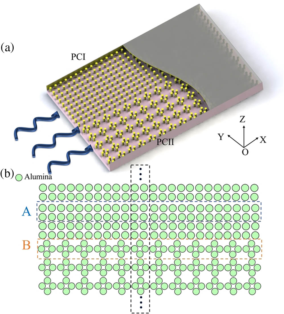
Figure 1 is a schematic of a 2D dielectric PC with a square lattice in a metallic waveguide. Four dielectric cylinders embedded in an air background in a unit cell of PCI do not have any rotation, while PCII possesses a 45° rotation compared to PCI. A stable light propagation protected by the topology can be obtained on the interface of two PCs with distinct topological properties. A 2D plane schematic of the PC structure is displayed in Fig. 1(b), where there is board with three upper PCI rows and three lower PCII rows, in which the dielectric material is alumina (green circles).
Sign up for Photonics Research TOC. Get the latest issue of Photonics Research delivered right to you!Sign up now
Figure 1.(a) Schematic diagram of the designed PC structure. A light beam transmits at the junction of PCI and PCII. (b) 2D plane schematic of PCs with different degrees of rotation in the unit cell.
To analyze the topological properties of the designed PCs, we calculated their band structures. Figures 2(a) and 2(d) display the unit cells of PCI (corresponding to 0°) and PCII (corresponding to 45°), composed of four dielectric cylinders located at four corners. The lattice constant of the PC is , the radius of alumina cylinders is , and the relative dielectric permittivity of dielectric material is [27]. We plotted dashed lines as the motion path of the four cylinders, which rotate against their center along the dotted line in one direction, as shown in Figs. 2(b) and 2(e). The black solid and dotted circles correspond, respectively, to the initial and final movement position of the PC dielectric cylinders. To control the position of the cylinders more precisely, we introduce a rotation parameter , and define , in which is the movement distance of the cylinders. Compared to PCI (), the cylinders of PCII move ; i.e., . Therefore, the variation in the PC structure is closely connected to the rotation parameter .
Figure 2.(a) and (b) Schematic of a unit cell of PCI () with four alumina cylinders at four corners. The lattice constant is , the radius of dielectric cylinders is , and the relative dielectric permittivity is . (c) Band diagram of PCI. Inset: first Brillouin zone. Right panel: distributions of eigen-electric fields at highly symmetric points. The parities of the bulk band are marked by “” and “−” signs. The photonic band gap (gray region) is topologically trivial. (d) and (e) Unit cell of PCII () with rotating dielectric cylinders. (f) A topological nontrivial band gap appears between the S1 and S2 bands highlighted in yellow. (g) Size of photonic band gap as a function of rotation parameter .
The TM (with polarization) band diagram of PCI () is plotted in Fig. 2(c), calculated by the commercial finite element method solver COMSOL Multiphysics. The first Brillouin zone is shown in the inset. We define the scanning path as , and three paths are controlled by piecewise function. The frequency sweeping follows the path function. In addition, we set two pairs of Floquet periodic conditions around the cell in the x axis and y axis directions. The intra- and interunit cell distances between the neighboring cylinders control the band topology. The intradistance is equal to the interdistance for PCI, so that it corresponds to the critical point of the topological phase transition. The first three bands of PCI are degenerated. There is a full trivial photonic band gap in PCI at a high frequency between the fourth and fifth bands. The operation of rotating dielectric cylinders opens a full gap at the S1 and S2 bands, as shown in Fig. 2(f) for PCII. The band topology can be encoded by their parities at highly symmetric points, which are the eigenvalues of the inversion symmetry operator [23–28]. The odd and even parities are indicated, respectively, by “” and “−”. We plot the electric field distributions at the M and X points of the S0 and S1 bands in the right panels. The inversion of the parities of the bulk bands demonstrates that the photonic band gap between S1 and S2 is topologically nontrivial; this is highlighted in Fig. 2(f) by the yellow region between 10 and 12 GHz. The topological phase of the PC can be characterized by the 2D Zak phase , which is defined as an integration of Berry connection over the first Brillouin zone: where the Berry connection is , in which and run over all occupied bands, and is the periodic Bloch function for the -th band [23,25]. The 2D Zak phase is related to bulk polarization [23], and corresponds to the value of 2D Zak phase. Based on the analysis of the parities of the bulk bands, the 2D Zak phase equals (0, 0) for , corresponding to a topologically trivial band gap at a high frequency. While , the Zak phase equals (, ), yielding topologically nontrivial band gaps. There is phase difference between the trivial and nontrivial. In addition, when equals the other values, the 2D Zak phase also equals (, ). As the rotation angle of PC cylinders increases, the band gap changes in Fig. 2(g). In addition, we plot the distributions of electric fields with S0, S1, and S2.
By stacking PCI () and PCII () with a common photonic band gap but distinct topological properties, topological edge states emerge at their interface. According to the method of supercell marked by a rectangle in Fig. 1(b), the calculated projected bands of PCs with different rotation parameters are shown in Fig. 3(a), where the green regions represent the bulk bands. We draw the separate transmission bands of the other four channels (10.991, 10.21, 9.68, 9.34 GHz) in Fig. 3(a), and the four energy bands are not related to the background. Figure 3(a) only shows the positions of four energy bands, which correspond to the simulated transmission frequency. The nearly flat edge state dispersions marked by a solid black line can be found around 10.321 GHz for PC structures composed of and 0.5. The simulations are performed to characterize the propagating properties of topological edge states. The designed structure with a single channel is displayed in Fig. 3(b), in which PCI is located at the upper part and PCII is located at the bottom part. The simulated domain contains arrays of dielectric cylinders. A stable and strong electric field is confined along the interface, which demonstrates that the transport of the edge states is obtained; therefore, we can construct a specific beam channel using topological trivial and nontrivial PCs. After controlling the finite width of the topological array, the two edge states along the interface cannot couple together and remain independent.
Figure 3.(a) Projected band for PCI () and PCII () structures. Topological edge state dispersions are denoted by solid lines in the photonic band gap. The green regions indicate bulk bands. (b) Simulated results show a stable and strong electric field on the interface. (c) The eigenmode distribution of the edge state at frequency with . The electric field is mainly concentrated at the interface.
To achieve better directional propagation of a specific beam, we designed a more complex PC structure consisting of gradient cylindrical arrays. As shown in Fig. 4(a), the rotation parameter gradually increases from the bottom to top sides of the proposed structure, and is equal to 0.1, 0.2, 0.3, 0.4, and 0.5, respectively. There are four optical channels to distinguish the different wavelengths of light, which are named as channel 0, channel 1, channel 2, and channel 3. There is strong independence in these channels with the stationary propagation frequencies, as shown in the Fig. 3(a). Moreover, there could be a few weak couplings of these channels. These channel couplings have tiny effects on their transmission. Figure 3(a) displays the projected band of these four channels highlighted by different colored lines, which are constructed by PCs with , , , and , respectively. Interestingly, different transport of the edge states can be realized with different frequency ranges. We understand these channels as the transition state of the initial topological boundary state, as shown in Fig. 3. The original symmetry of the structure about the x-axis and y-axis is destroyed by the influence of the rotation in the unit; it is a change process from a topological trivial state to a nontrivial state. The transmission frequency of the transition states exists in the energy bands of the topological edge states, and they will not exceed the top of the band gap and not fall below the bottom of the band gap. They are composed of different arrays of rotating units, and they hold the Zak phase with . Different rotation states can influence each other and produce topological boundary state light transmission. Figure 4(c) shows the transmission spectrum, in which four different colored areas represent four transport channels. The transmissions of these channels almost reach 1. The simulated electric field distributions for the four channels exhibit strong light transmission properties and frequency selectivity, as displayed in Fig. 4(b). When the incident beam impinges on the PCs, the edge states propagate in channel 0 at 9.34 GHz, channel 1 at 9.66 GHz, channel 2 at 10.12 GHz, and channel 3 at 10.94 GHz.
Figure 4.(a) 3D schematic of multichannel WDM device constructed by PCs with , 0.2, 0.3, 0.4, and 0.5. (b) Simulated results of the strong electric field distributions in channels 0, 1, 2, and 3 at 9.34, 9.67, 10.12, and 10.94 GHz, respectively. (b) Transmittance of the multichannel WDM device. The four colored areas represent the four channels, in which the transmittance is close to 1.
To demonstrate the topological transport of the edge states in the experiments, we fabricated PCI and PCII structures consisting of alumina cylinders with a relative dielectric permittivity of , as shown in Fig. 5(a). The other parameters of the fabricated PCs are the same in the simulations. These structures are pure-dielectric PCs and the Ohmic-loss effect can be neglected compared to plasmonic and metallic materials. The size of the experimental sample is , and five rows of alumina array are distributed on both sides of the interface. Figure 5(b) shows the simulated electric field and optical transmission at . The PCs are placed at a waveguide composed of two parallel metallic plates in the measurements and are surrounded by absorbing materials to avoid being affected by scattering. The excitation source marked by a star in Fig. 5(a) is set at the left side of the PCs. Based on the experimental method of the near-field scanning, we obtained the distribution of the out-of-plane electric field and the notable boundary optical transmission. The topological edge state emerges at 10.5 GHz, which shifts to a high frequency compared to the simulations. The experimental equipment and environmental conditions cause the difference in the frequency between the experimental and simulated results.
Figure 5.(a) Photograph of the experimental setup consisting of alumina cylinders with relative dielectric permittivity . (b) Simulated electric field of the topological edge state at . (c) Experimental measurement of the edge state at . The strong electric field localizes at the interface channel.
Considering the practicality of WDMs, we designed and fabricated a square waveguide using patterns of PCs with , 0.4, 0.3, 0.2, and 0.1. The experimental setup of the waveguide is shown in Fig. 6(a). The multichannel WDM device has been divided into three channels. At the same time, to facilitate the experimental measurement and production process, the overall size of the array was also improved. The simulations of electric field distributions and light transmissions are plotted in Figs. 6(b)–6(d) corresponding to channels 1–3 at 9.67, 10.25, and 10.98 GHz, respectively. Three channels individually and stably exhibit powerful control and transport of the light, demonstrating the propagating properties of the edge states. The source is set at the edge of the lower left corner of simulated domain, the light source is an antenna that is concentrated at one point, and the emission frequency range is 9–12 GHz. Our square array PC structure plays an important role in photonic integrated circuits and optical beam splitting. We further do an experiment to achieve a multichannel WDM device. The size of the PC array is . Figures 6(e)–6(g) show the experimental electric fields of three channels at 9.41, 10.27, and 10.79 GHz, respectively, which indicate a remarkable optical transmission path. In our simulations and experiments, all the electric field distributions have phase. Overall, the experimental results are in good agreement with the simulated results. Our integrated design provides flexibility for the application of optical beam splitting and it also is helpful to reduce light loss and leakage. These results support the idea that optical transmission can be successfully achieved in a complex PC structure and multichannel WDM device.
Figure 6.Simulation results of square three-channel WDM. (a) Array board with a size of . They individually and stably exhibit powerful control and transport of light, which correspond to (b) , (c) , and (d) . (e), (f) and (g) Optical transmission with three channels based on experimental data. The frequencies are 9.41 GHz, 10.27 GHz, and 10.79 GHz, respectively.
In this paper, we have proposed a kind of multichannel WDM device working in the microwave region. It is implemented by 2D topological PCs consisting of rotating cylinders, in which the edge states can effectively improve the quality of the transmitted light. We first analyzed the topological properties of bulk bands of PCs, then calculated the electric field distributions of topological edge states, and showed a clear path of light that is generated by our designed PC array. In addition, the application of the WDM is realized by using different channels with different degrees of rotation of the PC cylinders. The electric field distributions of the designed array device are simulated and experimentally measured, which agree well with each other. Our work may find more potential applications for beam sensing and biological detections in the future, and also contributes to the further understanding of optical edge states.