Reviews|140 Article(s)
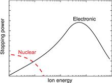
Modulating properties by light ion irradiation: From novel functional materials to semiconductor power devices
Ye Yuan, Shengqiang Zhou, and Xinqiang Wang
In this review, the application of light ion irradiation is discussed for tailoring novel functional materials and for improving the performance in SiC or Si based electrical power devices. The deep traps and electronic disorder produced by light ion irradiation can modify the electrical, magnetic, and optical properties of films (e.g., dilute ferromagnetic semiconductors and topological materials). Additionally, benefiting from the high reproducibility, precise manipulation of functional depth and density of defects, as well as the flexible patternability, the helium or proton ion irradiation has been successfully employed in improving the dynamic performance of SiC and Si based PiN diode power devices by reducing their majority carrier lifetime, although the static performance is sacrificed due to deep level traps. Such a trade-off has been regarded as the key point to compromise the static and dynamic performances of power devices. As a result, herein the light ion irradiation is highlighted in both exploring new physics and optimizing the performance in functional materials and electrical devices. In this review, the application of light ion irradiation is discussed for tailoring novel functional materials and for improving the performance in SiC or Si based electrical power devices. The deep traps and electronic disorder produced by light ion irradiation can modify the electrical, magnetic, and optical properties of films (e.g., dilute ferromagnetic semiconductors and topological materials). Additionally, benefiting from the high reproducibility, precise manipulation of functional depth and density of defects, as well as the flexible patternability, the helium or proton ion irradiation has been successfully employed in improving the dynamic performance of SiC and Si based PiN diode power devices by reducing their majority carrier lifetime, although the static performance is sacrificed due to deep level traps. Such a trade-off has been regarded as the key point to compromise the static and dynamic performances of power devices. As a result, herein the light ion irradiation is highlighted in both exploring new physics and optimizing the performance in functional materials and electrical devices.
Journal of Semiconductors
- Publication Date: Jun. 01, 2022
- Vol. 43, Issue 6, 063101 (2022)


Graphene synthesis, fabrication, characterization based on bottom-up and top-down approaches: An overview
Agbolade Lukman Olatomiwa, Tijjani Adam, Subash C. B. Gopinath, Sanusi Yekinni Kolawole, Oyeshola Hakeem Olayinka, and U. Hashim
This study presents an overview on graphene synthesis, fabrication and different characterization techniques utilized in the production. Since its discovery in 2004 by Andre Geim and Kostya Novoselov several research articles have been published globally to this effect, owing to graphene’s extraordinary, and exclusive characteristics which include optical transparency, excellent thermal, and mechanical properties. The properties and applications of this two-dimensional carbon crystal composed of single-layered material have created new avenues for the development of high-performance future electronics and technologies in energy storage and conversion for the sustainable energy. However, despite its potential and current status globally the difficulty in the production of monolayer graphene sheet still persists. Therefore, this review highlighted two approaches in the synthesis of graphene, which are the top-down and bottom-up approaches and examined the advantages and failings of the methods involved. In addition, the prospects and failings of these methods are investigated, as they are essential in optimizing the production method of graphene vital for expanding the yield, and producing high-quality graphene. This study presents an overview on graphene synthesis, fabrication and different characterization techniques utilized in the production. Since its discovery in 2004 by Andre Geim and Kostya Novoselov several research articles have been published globally to this effect, owing to graphene’s extraordinary, and exclusive characteristics which include optical transparency, excellent thermal, and mechanical properties. The properties and applications of this two-dimensional carbon crystal composed of single-layered material have created new avenues for the development of high-performance future electronics and technologies in energy storage and conversion for the sustainable energy. However, despite its potential and current status globally the difficulty in the production of monolayer graphene sheet still persists. Therefore, this review highlighted two approaches in the synthesis of graphene, which are the top-down and bottom-up approaches and examined the advantages and failings of the methods involved. In addition, the prospects and failings of these methods are investigated, as they are essential in optimizing the production method of graphene vital for expanding the yield, and producing high-quality graphene.
Journal of Semiconductors
- Publication Date: Jun. 01, 2022
- Vol. 43, Issue 6, 061101 (2022)
Characterization of interfaces: Lessons from the past for the future of perovskite solar cells
Wanlong Wang, Dongyang Zhang, Rong Liu, Deepak Thrithamarassery Gangadharan, Furui Tan, and Makhsud I. Saidaminov
A photovoltaic technology historically goes through two major steps to evolve into a mature technology. The first step involves advances in materials and is usually accompanied by the rapid improvement of power conversion efficiency. The second step focuses on interfaces and is usually accompanied by significant stability improvement. As an emerging generation of photovoltaic technology, perovskite solar cells are transitioning to the second step of their development when a significant focus shifts toward interface studies and engineering. While various interface engineering strategies have been developed, interfacial characterization is crucial to show the effectiveness of interfacial modification. Here, we review the characterization techniques that have been utilized in studying interface properties in perovskite solar cells. We first summarize the main roles of interfaces in perovskite solar cells, and then we discuss some typical characterization methodologies for morphological, optical, and electrical studies of interfaces. Successful experiences and existing problems are analyzed when discussing some commonly used methods. We then analyze the challenges and provide an outlook for further development of interfacial characterizations. This review aims to evoke strengthened research devotion on novel and persuasive interfacial engineering. A photovoltaic technology historically goes through two major steps to evolve into a mature technology. The first step involves advances in materials and is usually accompanied by the rapid improvement of power conversion efficiency. The second step focuses on interfaces and is usually accompanied by significant stability improvement. As an emerging generation of photovoltaic technology, perovskite solar cells are transitioning to the second step of their development when a significant focus shifts toward interface studies and engineering. While various interface engineering strategies have been developed, interfacial characterization is crucial to show the effectiveness of interfacial modification. Here, we review the characterization techniques that have been utilized in studying interface properties in perovskite solar cells. We first summarize the main roles of interfaces in perovskite solar cells, and then we discuss some typical characterization methodologies for morphological, optical, and electrical studies of interfaces. Successful experiences and existing problems are analyzed when discussing some commonly used methods. We then analyze the challenges and provide an outlook for further development of interfacial characterizations. This review aims to evoke strengthened research devotion on novel and persuasive interfacial engineering.
Journal of Semiconductors
- Publication Date: May. 01, 2022
- Vol. 43, Issue 5, 051202 (2022)

Multifunctional neurosynaptic devices for human perception systems
Wei Wen, Yunlong Guo, and Yunqi Liu
The traditional Von Neumann architecture for processing information is difficult to meet the needs of the big data era, while low-power, small-sized neurosynaptic devices can operate and store information, so that they have received extensive attention. Due to the development of artificial intelligence and robotics, neurosynaptic devices have been given high expectations and requirements. The trend of functionalization, intelligence, and integration of computing and storage is obvious. In this review, the basic principles and types of neurosynaptic devices are summarized, the achievements of neurosynaptic devices for human perception systems are discussed and a prospect on the development trend is also given. The traditional Von Neumann architecture for processing information is difficult to meet the needs of the big data era, while low-power, small-sized neurosynaptic devices can operate and store information, so that they have received extensive attention. Due to the development of artificial intelligence and robotics, neurosynaptic devices have been given high expectations and requirements. The trend of functionalization, intelligence, and integration of computing and storage is obvious. In this review, the basic principles and types of neurosynaptic devices are summarized, the achievements of neurosynaptic devices for human perception systems are discussed and a prospect on the development trend is also given.
Journal of Semiconductors
- Publication Date: May. 01, 2022
- Vol. 43, Issue 5, 051201 (2022)
Recent progress on advanced transmission electron microscopy characterization for halide perovskite semiconductors
Xiaomei Wu, Xiaoxing Ke, and Manling Sui
Halide perovskites are strategically important in the field of energy materials. Along with the rapid development of the materials and related devices, there is an urgent need to understand the structure–property relationship from nanoscale to atomic scale. Much effort has been made in the past few years to overcome the difficulty of imaging limited by electron dose, and to further extend the investigation towards operando conditions. This review is dedicated to recent studies of advanced transmission electron microscopy (TEM) characterizations for halide perovskites. The irradiation damage caused by the interaction of electron beams and perovskites under conventional imaging conditions are first summarized and discussed. Low-dose TEM is then discussed, including electron diffraction and emerging techniques for high-resolution TEM (HRTEM) imaging. Atomic-resolution imaging, defects identification and chemical mapping on halide perovskites are reviewed. Cryo-TEM for halide perovskites is discussed, since it can readily suppress irradiation damage and has been rapidly developed in the past few years. Finally, the applications of in-situ TEM in the degradation study of perovskites under environmental conditions such as heating, biasing, light illumination and humidity are reviewed. More applications of emerging TEM characterizations are foreseen in the coming future, unveiling the structural origin of halide perovskite’s unique properties and degradation mechanism under operando conditions, so to assist the design of a more efficient and robust energy material. Halide perovskites are strategically important in the field of energy materials. Along with the rapid development of the materials and related devices, there is an urgent need to understand the structure–property relationship from nanoscale to atomic scale. Much effort has been made in the past few years to overcome the difficulty of imaging limited by electron dose, and to further extend the investigation towards operando conditions. This review is dedicated to recent studies of advanced transmission electron microscopy (TEM) characterizations for halide perovskites. The irradiation damage caused by the interaction of electron beams and perovskites under conventional imaging conditions are first summarized and discussed. Low-dose TEM is then discussed, including electron diffraction and emerging techniques for high-resolution TEM (HRTEM) imaging. Atomic-resolution imaging, defects identification and chemical mapping on halide perovskites are reviewed. Cryo-TEM for halide perovskites is discussed, since it can readily suppress irradiation damage and has been rapidly developed in the past few years. Finally, the applications of in-situ TEM in the degradation study of perovskites under environmental conditions such as heating, biasing, light illumination and humidity are reviewed. More applications of emerging TEM characterizations are foreseen in the coming future, unveiling the structural origin of halide perovskite’s unique properties and degradation mechanism under operando conditions, so to assist the design of a more efficient and robust energy material.
Journal of Semiconductors
- Publication Date: Apr. 01, 2022
- Vol. 43, Issue 4, 041106 (2022)

Structural evolution of low-dimensional metal oxide semiconductors under external stress
Peili Zhao, Lei Li, Guoxujia Chen, Xiaoxi Guan, Ying Zhang, Weiwei Meng, Ligong Zhao, Kaixuan Li, Renhui Jiang, Shuangfeng Jia, He Zheng, and Jianbo Wang
Metal oxide semiconductors (MOSs) are attractive candidates as functional parts and connections in nanodevices. Upon spatial dimensionality reduction, the ubiquitous strain encountered in physical reality may result in structural instability and thus degrade the performance of MOS. Hence, the basic insight into the structural evolutions of low-dimensional MOS is a prerequisite for extensive applications, which unfortunately remains largely unexplored. Herein, we review the recent progress regarding the mechanical deformation mechanisms in MOSs, such as CuO and ZnO nanowires (NWs). We report the phase transformation of CuO NWs resulting from oxygen vacancy migration under compressive stress and the tensile strain-induced phase transition in ZnO NWs. Moreover, the influence of electron beam irradiation on interpreting the mechanical behaviors is discussed. Metal oxide semiconductors (MOSs) are attractive candidates as functional parts and connections in nanodevices. Upon spatial dimensionality reduction, the ubiquitous strain encountered in physical reality may result in structural instability and thus degrade the performance of MOS. Hence, the basic insight into the structural evolutions of low-dimensional MOS is a prerequisite for extensive applications, which unfortunately remains largely unexplored. Herein, we review the recent progress regarding the mechanical deformation mechanisms in MOSs, such as CuO and ZnO nanowires (NWs). We report the phase transformation of CuO NWs resulting from oxygen vacancy migration under compressive stress and the tensile strain-induced phase transition in ZnO NWs. Moreover, the influence of electron beam irradiation on interpreting the mechanical behaviors is discussed.
Journal of Semiconductors
- Publication Date: Apr. 01, 2022
- Vol. 43, Issue 4, 041105 (2022)
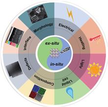
In-situ monitoring of dynamic behavior of catalyst materials and reaction intermediates in semiconductor catalytic processes
Zhen Fang, Yao Liu, Chengyi Song, Peng Tao, Wen Shang, Tao Deng, Xiaoqin Zeng, and Jianbo Wu
Semiconductor photocatalysis, as a key part of solar energy utilization, has far-reaching implications for industrial, agricultural, and commercial development. Lack of understanding of the catalyst evolution and the reaction mechanism is a critical obstacle for designing efficient and stable photocatalysts. This review summarizes the recent progress of in-situ exploring the dynamic behavior of catalyst materials and reaction intermediates. Semiconductor photocatalytic processes and two major classes of in-situ techniques that include microscopic imaging and spectroscopic characterization are presented. Finally, problems and challenges in in-situ characterization are proposed, geared toward developing more advanced in-situ techniques and monitoring more accurate and realistic reaction processes, to guide designing advanced photocatalysts. Semiconductor photocatalysis, as a key part of solar energy utilization, has far-reaching implications for industrial, agricultural, and commercial development. Lack of understanding of the catalyst evolution and the reaction mechanism is a critical obstacle for designing efficient and stable photocatalysts. This review summarizes the recent progress of in-situ exploring the dynamic behavior of catalyst materials and reaction intermediates. Semiconductor photocatalytic processes and two major classes of in-situ techniques that include microscopic imaging and spectroscopic characterization are presented. Finally, problems and challenges in in-situ characterization are proposed, geared toward developing more advanced in-situ techniques and monitoring more accurate and realistic reaction processes, to guide designing advanced photocatalysts.
Journal of Semiconductors
- Publication Date: Apr. 01, 2022
- Vol. 43, Issue 4, 041104 (2022)
Study of structure-property relationship of semiconductor nanomaterials by off-axis electron holography
Luying Li, Yongfa Cheng, Zunyu Liu, Shuwen Yan, Li Li, Jianbo Wang, Lei Zhang, and Yihua Gao
As the scaling down of semiconductor devices, it would be necessary to discover the structure-property relationship of semiconductor nanomaterials at nanometer scale. In this review, the quantitative characterization technique off-axis electron holography is introduced in details, followed by its applications in various semiconductor nanomaterials including group IV, compound and two-dimensional semiconductor nanostructures in static states as well as under various stimuli. The advantages and disadvantages of off-axis electron holography in material analysis are discussed, the challenges facing in-situ electron holographic study of semiconductor devices at working conditions are presented, and all the possible influencing factors need to be considered to achieve the final goal of fulfilling quantitative characterization of the structure-property relationship of semiconductor devices at their working conditions. As the scaling down of semiconductor devices, it would be necessary to discover the structure-property relationship of semiconductor nanomaterials at nanometer scale. In this review, the quantitative characterization technique off-axis electron holography is introduced in details, followed by its applications in various semiconductor nanomaterials including group IV, compound and two-dimensional semiconductor nanostructures in static states as well as under various stimuli. The advantages and disadvantages of off-axis electron holography in material analysis are discussed, the challenges facing in-situ electron holographic study of semiconductor devices at working conditions are presented, and all the possible influencing factors need to be considered to achieve the final goal of fulfilling quantitative characterization of the structure-property relationship of semiconductor devices at their working conditions.
Journal of Semiconductors
- Publication Date: Apr. 01, 2022
- Vol. 43, Issue 4, 041103 (2022)
Comprehensive,in operando, and correlative investigation of defects and their impact on device performance
Yong Zhang, and David J. Smith
Despite the long history of research that has focused on the role of defects on device performance, the studies have not always been fruitful. A major reason is because these defect studies have typically been conducted in a parallel mode wherein the semiconductor wafer was divided into multiple pieces for separate optical and structural characterization, as well as device fabrication and evaluation. The major limitation of this approach was that either the defect being investigated by structural characterization techniques was not the same defect that was affecting the device performance or else the defect was not characterized under normal device operating conditions. In this review, we describe a more comprehensive approach to defect study, namely a series mode, using an array of spatially-resolved optical, electrical, and structural characterization techniques, all at the individual defect level but applied sequentially on a fabricated device. This novel sequential approach enables definitive answers to key questions, such as: (i) how do individual defects affect device performance? (ii) how does the impact depend on the device operation conditions? (iii) how does the impact vary from one defect to another? Implementation of this different approach is illustrated by the study of individual threading dislocation defects in GaAs solar cells. Additionally, we briefly describe a 3-D Raman thermometry method that can also be used for investigating the roles of defects in high power devices and device failure mechanisms. Despite the long history of research that has focused on the role of defects on device performance, the studies have not always been fruitful. A major reason is because these defect studies have typically been conducted in a parallel mode wherein the semiconductor wafer was divided into multiple pieces for separate optical and structural characterization, as well as device fabrication and evaluation. The major limitation of this approach was that either the defect being investigated by structural characterization techniques was not the same defect that was affecting the device performance or else the defect was not characterized under normal device operating conditions. In this review, we describe a more comprehensive approach to defect study, namely a series mode, using an array of spatially-resolved optical, electrical, and structural characterization techniques, all at the individual defect level but applied sequentially on a fabricated device. This novel sequential approach enables definitive answers to key questions, such as: (i) how do individual defects affect device performance? (ii) how does the impact depend on the device operation conditions? (iii) how does the impact vary from one defect to another? Implementation of this different approach is illustrated by the study of individual threading dislocation defects in GaAs solar cells. Additionally, we briefly describe a 3-D Raman thermometry method that can also be used for investigating the roles of defects in high power devices and device failure mechanisms.
Journal of Semiconductors
- Publication Date: Apr. 01, 2022
- Vol. 43, Issue 4, 041102 (2022)
In-situ/operando characterization techniques for organic semiconductors and devices
Sai Jiang, Qinyong Dai, Jianhang Guo, and Yun Li
The increasing demands of multifunctional organic electronics require advanced organic semiconducting materials to be developed and significant improvements to be made to device performance. Thus, it is necessary to gain an in-depth understanding of the film growth process, electronic states, and dynamic structure-property relationship under realistic operation conditions, which can be obtained by in-situ/operando characterization techniques for organic devices. Here, the up-to-date developments in the in-situ/operando optical, scanning probe microscopy, and spectroscopy techniques that are employed for studies of film morphological evolution, crystal structures, semiconductor-electrolyte interface properties, and charge carrier dynamics are described and summarized. These advanced technologies leverage the traditional static characterizations into an in-situ and interactive manipulation of organic semiconducting films and devices without sacrificing the resolution, which facilitates the exploration of the intrinsic structure-property relationship of organic materials and the optimization of organic devices for advanced applications. The increasing demands of multifunctional organic electronics require advanced organic semiconducting materials to be developed and significant improvements to be made to device performance. Thus, it is necessary to gain an in-depth understanding of the film growth process, electronic states, and dynamic structure-property relationship under realistic operation conditions, which can be obtained by in-situ/operando characterization techniques for organic devices. Here, the up-to-date developments in the in-situ/operando optical, scanning probe microscopy, and spectroscopy techniques that are employed for studies of film morphological evolution, crystal structures, semiconductor-electrolyte interface properties, and charge carrier dynamics are described and summarized. These advanced technologies leverage the traditional static characterizations into an in-situ and interactive manipulation of organic semiconducting films and devices without sacrificing the resolution, which facilitates the exploration of the intrinsic structure-property relationship of organic materials and the optimization of organic devices for advanced applications.
Journal of Semiconductors
- Publication Date: Apr. 01, 2022
- Vol. 43, Issue 4, 041101 (2022)
© Copyright 2018-2021 | Chinese Laser Press. All Rights Reserved 沪ICP备15018463号-20