
Wanlong Wang, Dongyang Zhang, Rong Liu, Deepak Thrithamarassery Gangadharan, Furui Tan, Makhsud I. Saidaminov. Characterization of interfaces: Lessons from the past for the future of perovskite solar cells[J]. Journal of Semiconductors, 2022, 43(5): 051202
- Journal of Semiconductors
- Vol. 43, Issue 5, 051202 (2022)
Abstract
1. Introduction
The simplest solar cell is a sandwich of at least four materials (front electrode, p- and n-semiconductors, and back electrode) with at least five interfaces (three between materials, and front and back surfaces). As solar cells are developed, they will involve more layers and interfaces: for instance, the best Si solar cell consists of p–n junction layers and passivasive interfaces[
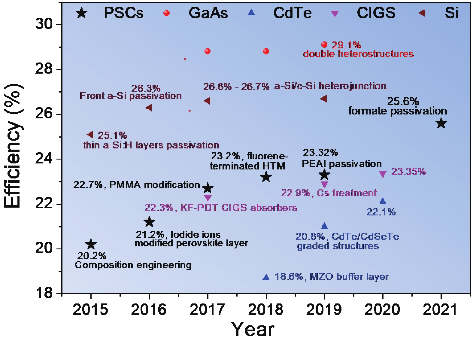
Interface engineering has played a significant role in mature photovoltaic technologies (Fig. 1). For example, the Si solar cell with a record efficiency of 26.7% PCE was achieved by extensive interface passivations: an n-type crystalline Si (c-Si) was passivated by p+ heterojunction layer stack (i.e., a-Si:H layer deposition followed by p:a-Si:H layer deposition) from one side and n+ heterojunction layer stack (i.e., a-Si:H layer deposition followed by n-type thin-film Si layer deposition) from the other side[
![]()
Figure 1.(Color online) Efficiency evolution of different solar cells. Interface engineering has recently played an increasingly important role in obtaining a higher efficiency for each cell.
For the emerging perovskite photovoltaics, halide perovskite now undergoes rapid advance to a higher efficiency, and a better stability and scalability[
However, it is known that the interface is formed between two heteromaterials and usually spans over only several atomic layers[
2. The role of interfaces for perovskite solar cells
It is known that interface of a perovskite solar cell impacts the performance of the device (e.g., the excitation information, separation, and recombination). Furthermore, the degradation of a device is also highly sensitive to the interface. An experimental point of view showed that interfacial defects in PSCs were relevant with such these key issues, such as instability[
2.1. Oxygen infiltration
Interfaces in PSCs affect their chemical stability[
2.2. Humidity corrosion
Compared to the oxygen penetration at the interface, moisture diffusion along the interface seems to be more detrimental. A great deal of research has reported performance degradation due to interface-related moisture corrosion[
2.3. Electronic behavior
As a key part of multilayer optoelectronic devices, the interfaces in perovskite solar cells mainly play a role in charge transfer extraction. An efficiency gap may result from nonradiative recombination (Fig. 2), energy mismatch and optical losses at the interface. During the transfer of charge between perovskite and CTL, a recombination of the carrier would occur. Interface engineering is required to reduce interfacial recombination losses[
![]()
Figure 2.(Color online) (a) Perovskite crystal structure, Schottky defect, Frenkel defect and ion migration through interfaces. (b) Schematic illustration of photo-generation and, diffusion and transfer of charges at interfaces, trap-assisted nonradiative recombination (due to intrinsic defects and impurities at interfaces) and back transfer and interface recombination. (c) Energy band alignment of some typical materials used in perovskite solar cells.
For charge transfer extraction, it is necessary to have a suitable energy-level alignment between transport layers and perovskite. This is vital to solar cell parameters, such as photovoltage and fill factor (FF)[
3. Interface characterization
Because the interfaces are ultrathin—probably within several atoms—and are deeply buried inside the device, it is difficult to carry out direct measurements on these parts. However, because of its importance, some characterization methods have been developed. In this part, we focus on some important characterization process that can reflect the morphological, optical, and electrical information of interfaces. We note that this is not an exhaustive list of characterization tools, but purposely covers the most relevant ones that might be useful for direct or indirect investigation of interfaces.
3.1. Morphology and composition characterization
Modern scanning electron microscopes (SEMs) have resolutions down to 1 nm. In SEMs, the fast incoming electrons supply energy to the atomic outer-shell electrons in the specimen, which is sufficient for the atomic electron to be released as a “secondary electron” (SE) whose images mainly show the surface structure (topography) of the specimen[
![]()
Figure 3.(Color online) Interface material characterization methods. (a) Cross-section SEM image of PSCs showing excess of PbI2 at interfaces. Reproduced with permission from Ref. [
Although obtained by optical measurements, photoluminescence (PL) mapping of a perovskite film can reflect the morphological and compositional information of the film, especially when the perovskite films contain multi-phases that show different in-situ PL properties. Different PL intensity and PL wavelengths usually indicate different phase distributions. Therefore, this characterization could be used to study the phase and crystallization properties in the hybrid. Zhao et al. studied the mixture of a perovskite solution and PbI2, and proved that the perovskite solution behaved as dispersed seed that showed distinct PL phenomenon in the PbI2 matrix. When fabricating the perovskite film by a typical two-step method, the as-existed perovskite seed benefited the crystallization of perovskite with large size. The entire process can be clearly demonstrated by in-situ PL mapping properties of the films (Fig. 3(b))[
An atomic force microscope (AFM) is a useful instrument with high atomic resolution that can detect the morphological properties of various materials and samples in the nanometer scale. Compared with a conventional microscope, AFM has the advantage of observing the sample surface with high magnification under atmospheric conditions. It can be used to detect the three-dimensional image of a sample’s surface. The roughness calculation, thickness, step width, block diagram and granularity analysis can also be obtained for the 3D morphology image. For example, Methawee Nukunudompanichet al. used different methods to prepare TiO2 electron transport layers and used AFM to characterize the surface roughness. The growth mechanism of perovskite grain on ETLs with different roughness was thus obtained based on the preliminary AFM characterization results at the interfaces (Fig. 3(c))[
A transmission electron microscope (TEM) can be used to observe fine structures smaller than 0.2 μm that cannot be seen under an optical microscope. These structures are called submicroscopic structures or ultrastructures. Because electrons are easily scattered or absorbed by objects, the penetration is low, and the density and thickness of samples will affect the final imaging quality. Therefore, ultrathin perovskite sections with a thickness within several tens of nanometers should be prepared. For interface characterization by TEM, usually cross-sectional sample containing interface part should be prepared and precisely targeted during TEM measurements. Like SEM, TEM is also a direct way to “see” the interface. For example, by high resolution TEM (HRTEM), the interfacial region could be tested to get useful information, such as thickness, location and, if aided by high-angle annular dark-field (HAADF) scanning TEM, the content of a certain atom (Fig. 3(d))[
X-ray photoelectron spectroscopy (XPS) is a very sensitive tool to characterize the composition of a film[
Time-of-flight secondary ion mass spectrometry (TOF-SIMS) is another useful method to measure the chemical distribution of the nanocomposite, the interface degradation and ion migration in the device[
When considering TOF-SIMS, one’s attention should be paid to the choice of tracking makers because some markers like benzene rings are not easy to detect. For example, when proving the existence of surface ultrathin modifiers, we found TOF-SIMS had difficulties in detecting characteristic group of benzene ring in molecules such as Spiro-OMeTAD or polyTPD, while the fluorine atom instead can be easily tracked[
3.2. Optical characterization
From this analysis, it can be seen that the morphology and component of the junction/interface part could be directly investigated by some professional measurements. However, it is not that easy to directly investigate the optoelectronic properties of the interfaces themselves. Optical characterization on the stacked layers usually aims at the influence of the interfaces on the physical properties of an adjacent perovskite layer. In this part, we show some optical characterizations that can reflect the role of interfaces.
PL, including steady state and time resolved PL (TRPL) spectra, is a commonly used method. Typically, PL characterization on perovskite films with buffer layers (contain heterojunction interfaces) can demonstrate the influence of interfaces, crystallization quality (defect density) of the entire perovskite film or the contact region. Buffer layer-induced contact passivation or enhanced crystallization (that means less defect states or grain boundaries) usually enables an enhanced PL intensity and elongated PL lifetime, while a blue shift of the peak is indicative of the decrease in spontaneous nonradiative recombination from the trap states[
![]()
Figure 4.(Color online) (a) Steady state and (b) time resolved photoluminescence (PL) spectra of perovskite films with different back contact layers. Reproduced with permission from Ref. [
In our opinion, if a charge (either holes or electrons) acceptor buffer layer with passivasive surface is adopted to form contact with perovskite, then one should pay special attention to the conclusion made from PL and TRPL results because both passivation effect (cause enlarged PL intensity and TRPL lifetime) and charge transfer effect (cause decreased PL intensity and TRPL lifetime) exist in this contact[
Besides the photoluminescence spectrum, transient absorption spectroscopy (TAS) is a powerful technique that allows studying carrier dynamics both in bulk film and at interfaces. The change in light absorption or reflection is recorded by adjusting the time interval between the pump pulse and the probe pulse arriving at the sample. In addition, TAS provides indirect information on contact interfaces by measuring the absorption behaviors of perovskite film itself[
For the interface contact for solar cell application, energy-level alignments at the interface play a critical role in charge dynamics. An ultraviolet photoelectron spectrometer (UPS) is frequently used to evaluate this key parameter. Because the energy of UV excitation light source is low, it can only ionize the valence electrons and valence band electrons in the outer electronic orbit of atoms, and can distinguish the vibrational energy levels of molecules. The penetration/detection depth during UPS measurement is as small as several (typically within 5 nm) nanometers. Therefore, to uncover the band alignment at the interface of two layers, one needs to carry out separate UPS measurement on each layer (Fig. 4(e))[
To enhance optical properties of perovskite films, effective light management is useful for increasing light absorption. An artificial structure with textured surface was thus developed to form contact with perovskite film[
3.3. Electrical characterization
As optoelectronic devices, perovskite solar cells mainly work on charge transfer and extraction at interfaces. Electrical characterization on these processes is of great importance. Compared to the main indirect optical measurements, electrical characterization on perovskite layers with heterojunction interfaces have proven to be more straightforward to get information of interfaces. In this part, we analyze some typical electrical methods that can directly reflect the properties of interfacial contact.
Transient photocurrent (TPC) characterization is a typical process to depict the charge transfer extraction at the perovskite interfaces. In a short circuit condition, the largest photocurrent output will drop after the transient light excitation disappears. The faster the photocurrent drops, the faster and more efficient the charges transfer extraction will be[
![]()
Figure 5.(Color online) (a) Transient photocurrent spectra of perovskite films with different contact thin layers. Reproduced with permission from Ref. [
In the open circuit condition, however, the neat photocurrent output is zero due to complete charge recombination—either via intrinsic electron/hole recombination or via trap state induced nonradiative recombination. In this model, photovoltage is usually tracked to evaluate the interfacial charge recombination because defect induced charge nonradiative recombination is much faster than the intrinsic recombination[
Electrochemical impendence spectrum (EIS) a similar characterization that can also reflect the interfacial charge dynamics at open circuit conditions. By varying the bias voltage applied on the perovskite solar cells, different charge behaviors can be modulated. EIS measurements are commonly adopted in dye-sensitized solar cells to show three distinct charge processes in the solar cells: charge collection by electrode (the fastest, high frequency), the interfacial charge transfer between sensitizer dye and nanoparticles (TiO2) (the modest, middle frequency), and charge transport in the liquid electrolyte (the slowest, low frequency)[
We have noted that, regarding the two typical charge behaviors (i.e., charge transfer separation/extraction and charge transfer recombination), the corresponding electrical characterization has mainly been carried out at either short circuit condition (charge transfer separation/extraction) or open circuit condition (charge transfer recombination). Considering that the electrochemical impendence at zero bias is usually too large to be regularly and precisely determined, some important interfacial information relating to charge transfer extraction might have been ignored in the previous literature. This speculation is yet to be uncovered.
As a facile I–V measurement, space-charge-limited current (SCLC) characterization has usually been adopted to evaluate some new HTLs or ETLs that can enable interfacial passivation except for its basic charge acceptor role[
Considering that the organic/inorganic hybrid perovskite materials is volatile and decomposable under exposure to strong optical, thermal, electrical or humidity stimulation, the optical and electrical measurements mentioned here have not contained very strong optical radiation or large electric fields. However, some characterization with very high space resolution ratio (which usually needs a focused stimulation source, such as an electron beam) can provide detailed measurements on precisely targeted interfaces. The electron beam induced current (EBIC) process was developed to measure the current mapping of cross-section including interfaces because we know that electron beam from sources like SEM chamber has high space resolution ratio[
4. Challenges and outlook
Interface modulation has played an increasingly important role in performance improvement and commercialization of perovskite solar cells, in which characterization of this critical component should be fully and persuasively developed. Our analysis of the presently reported interface-related techniques allows us to summarize several detailed problems that should be given attention when carrying out measurements on interfaces.
It was found that some interface-related conclusions were not persuasive based on inadequate characterizations. A typical example is the PL and TRPL research of the perovskite/buffer layer heterojunction, where improved charge transfer and contact passivation coexist. Additional experiments are needed to make two distinct effects clear: charge transfer caused a decrease in PL intensity and TRPL lifetime, and passivation induced enhancement in these two factors. Some characterization methods (e.g., electrochemical impedance spectrum) originated from other photovoltaic techniques. Therefore, their direct adoption for solid state perovskite thin-film solar cells might cause confusion when analyzing detailed charge dynamics at interfaces because there is no remarkable difference in the speed (frequency) of charge transfer and transport at different parts of a perovskite solar cell. A precise and stable impedance equipment with high time resolution is required to tell different kinetics apart.
Considering the intrinsic chemical and phase stability of perovskite, another challenge is to keep the perovskite phase as it is during various measurement conditions. Usually, perovskite samples would be tested in ambient air with a certain humidity and oxygen that will deteriorate the chemical and phase stability of perovskite materials. Optoelectronic measurements under intense light, high temperature or large electric field would also cause degradation, iron migration or phase variation in perovskite, which would influence the accuracy of measurement results correlated with interfaces.
A direct and more reliable characterization strategy is required to better serve the working mechanism of interface-related modulation. Simultaneous measurements on in-situ morphology together with intrinsic optoelectronic properties seem attractive in revealing interfacial species behaviors at a precise location. This might also require a robust sample preparation process that should present the real interface part while keeping its original properties. In addition, this research field would benefit more from a deeper study on how to characterize some interesting dynamical process when a solar cell is under work, such as electron transfer induced potential variation, field induced trap filling, or even light scattering by nanostructured interfaces.
5. Conclusions
Interface-related characterization techniques have played a major role in understanding the physical and chemical properties and evolution of PSCs. In this review, we have illustrated the importance of interface-characterization methods for PSC research. These techniques allow us to obtain insights of the nano- and microscale details of perovskite surfaces and interfaces. While some characterization techniques indeed provide insightful understanding of the interfaces, new strategic and reliable methods are still needed. This requires a thorough and full understanding of the nature of the interfaces, such as composition, morphology, defects, and stability. We have no doubt that these versatile tools will continue to enable the exploration of questions related to the micro and nano structures in PSCs, bringing these materials beyond the state-of-the-art.
Acknowledgements
This publication is based in part on the work supported by the Science and Technology Development Project of Henan Province (grant no. 202300410048), the Intelligence Introduction Plan of Henan Province in 2021 (CXJD2021008), the Postdoctoral Fund of China (grant no. FJ3050A0670111), the Henan University Fund, and the Canada Research Chairs Supplement Fund and New Frontiers in Research Fund (NFRF).
References
[1] T Dullweber, M Stöhr, C Kruse et al. Evolutionary PERC+ solar cell efficiency projection towards 24% evaluating shadow-mask-deposited poly-Si fingers below the Ag front contact as next improvement step. Sol Energy Mater Sol Cells, 212, 110586(2020).
[2] J Yu, M D Liao, D Yan et al. Activating and optimizing evaporation-processed magnesium oxide passivating contact for silicon solar cells. Nano Energy, 62, 181(2019).
[3] T G Allen, J Bullock, X B Yang et al. Passivating contacts for crystalline silicon solar cells. Nat Energy, 4, 914(2019).
[4] K Yoshikawa, H Kawasaki, W Yoshida et al. Silicon heterojunction solar cell with interdigitated back contacts for a photoconversion efficiency over 26%. Nat Energy, 2, 1(2017).
[5] T Kato, J L Wu, Y Hirai et al. Record efficiency for thin-film polycrystalline solar cells up to 22.9% achieved by Cs-treated Cu(In, Ga)(Se, S)2. IEEE J Photovolt, 9, 325(2019).
[6] W K Metzger, S Grover, D Lu et al. Exceeding 20% efficiency with
[7] J M Burst, J N Duenow, D S Albin et al. CdTe solar cells with open-circuit voltage breaking the 1 V barrier. Nat Energy, 1, 16015(2016).
[8] M A Green, Y Hishikawa, E D Dunlop et al. Solar cell efficiency tables (Version 53). Prog Photovolt: Res Appl, 27, 3(2019).
[9] M Jeong, I W Choi, E M Go et al. Stable perovskite solar cells with efficiency exceeding 24.8% and 0.3-V voltage loss. Science, 369, 1615(2020).
[10] T H Han, S Tan, J J Xue et al. Interface and defect engineering for metal halide perovskite optoelectronic devices. Adv Mater, 31, 1803515(2019).
[11] Y Bai, X Y Meng, S H Yang. Interface engineering for highly efficient and stable planar p-i-n perovskite solar cells. Adv Energy Mater, 8, 1701883(2018).
[12] P Schulz, D Cahen, A Kahn. Halide perovskites: Is it all about the interfaces. Chem Rev, 119, 3349(2019).
[13] F Zhang, K Zhu. Additive engineering for efficient and stable perovskite solar cells. Adv Energy Mater, 10, 1902579(2020).
[14] C T Zuo, H J Bolink, H W Han et al. Advances in perovskite solar cells. Adv Sci, 3, 1500324(2016).
[15] N J Jeon, H Na, E H Jung et al. A fluorene-terminated hole-transporting material for highly efficient and stable perovskite solar cells. Nat Energy, 3, 682(2018).
[16] Q Jiang, Y Zhao, X W Zhang et al. Surface passivation of perovskite film for efficient solar cells. Nat Photonics, 13, 460(2019).
[17] G Yang, Z W Ren, K Liu et al. Stable and low-photovoltage-loss perovskite solar cells by multifunctional passivation. Nat Photonics, 15, 681(2021).
[18] S Y Shao, M A Loi. The role of the interfaces in perovskite solar cells. Adv Mater Interfaces, 7, 1901469(2020).
[19] Y W Miao, M M Zheng, H X Wang et al.
[20] P Wang, F Cai, L Yang et al. Eliminating light-soaking instability in planar heterojunction perovskite solar cells by interfacial modifications. ACS Appl Mater Interfaces, 10, 33144(2018).
[21] F Zheng, X M Wen, T L Bu et al. Slow response of carrier dynamics in perovskite interface upon illumination. ACS Appl Mater Interfaces, 10, 31452(2018).
[22] W Chen, Y C Zhou, G C Chen et al. Alkali chlorides for the suppression of the interfacial recombination in inverted planar perovskite solar cells. Adv Energy Mater, 9, 1803872(2019).
[23] S B Xiong, T Hao, Y Y Sun et al. Defect passivation by nontoxic biomaterial yields 21% efficiency perovskite solar cells. J Energy Chem, 55, 265(2021).
[24] T S Sherkar, C Momblona, L Gil-Escrig et al. Recombination in perovskite solar cells: Significance of grain boundaries, interface traps, and defect ions. ACS Energy Lett, 2, 1214(2017).
[25] A M A Leguy, Y H Hu, M Campoy-Quiles et al. Reversible hydration of CH3NH3PbI3 in films, single crystals, and solar cells. Chem Mater, 27, 3397(2015).
[26] F Deng, X T Li, X Lv et al. Low-temperature processing all-inorganic carbon-based perovskite solar cells up to 11.78% efficiency via alkali hydroxides interfacial engineering. ACS Appl Energy Mater, 3, 401(2020).
[27] J H Wu, J J Shi, Y M Li et al. Quantifying the interface defect for the stability origin of perovskite solar cells. Adv Energy Mater, 9, 1901352(2019).
[28] T T Wu, C Zhen, H Z Zhu et al. Gradient Sn-doped heteroepitaxial film of faceted rutile TiO2 as an electron selective layer for efficient perovskite solar cells. ACS Appl Mater Interfaces, 11, 19638(2019).
[29] G X Wang, L P Wang, J H Qiu et al.
[30] H C Hsieh, C Y Hsiow, K F Lin et al. Analysis of defects and traps in N–I–P layered-structure of perovskite solar cells by charge-based deep level transient spectroscopy (Q-DLTS). J Phys Chem C, 122, 17601(2018).
[31] Z H Liu, L B Qiu, L K Ono et al. A holistic approach to interface stabilization for efficient perovskite solar modules with over 2, 000-hour operational stability. Nat Energy, 5, 596(2020).
[32] A Mahapatra, D Prochowicz, M M Tavakoli et al. A review of aspects of additive engineering in perovskite solar cells. J Mater Chem A, 8, 27(2020).
[33] S L Cao, H X Wang, H Y Li et al. Critical role of interface contact modulation in realizing low-temperature fabrication of efficient and stable CsPbIBr2 perovskite solar cells. Chem Eng J, 394, 124903(2020).
[34] M M Tavakoli, R Tavakoli, P Yadav et al. A graphene/ZnO electron transfer layer together with perovskite passivation enables highly efficient and stable perovskite solar cells. J Mater Chem A, 7, 679(2019).
[35] X P Zheng, Y Hou, C X Bao et al. Managing grains and interfaces via ligand anchoring enables 22.3%-efficiency inverted perovskite solar cells. Nat Energy, 5, 131(2020).
[36] Z F Wu, Z H Liu, Z H Hu et al. Highly efficient and stable perovskite solar cells via modification of energy levels at the perovskite/carbon electrode interface. Adv Mater, 31, 1804284(2019).
[37] M M Tavakoli, M Saliba, P Yadav et al. Synergistic crystal and interface engineering for efficient and stable perovskite photovoltaics. Adv Energy Mater, 9, 1802646(2019).
[38] J J Yoo, S Wieghold, M C Sponseller et al. An interface stabilized perovskite solar cell with high stabilized efficiency and low voltage loss. Energy Environ Sci, 12, 2192(2019).
[39] C C Boyd, R Cheacharoen, T Leijtens et al. Understanding degradation mechanisms and improving stability of perovskite photovoltaics. Chem Rev, 119, 3418(2019).
[40] A J Pearson, G E Eperon, P E Hopkinson et al. Oxygen degradation in mesoporous Al2O3/CH3NH3PbI3−
[41] N K Noel, S D Stranks, A Abate et al. Lead-free organic–inorganic tin halide perovskites for photovoltaic applications. Energy Environ Sci, 7, 3061(2014).
[42] J Y Seo, H S Kim, S Akin et al. Novel p-dopant toward highly efficient and stable perovskite solar cells. Energy Environ Sci, 11, 2985(2018).
[43] J Z Chen, N G Park. Inorganic hole transporting materials for stable and high efficiency perovskite solar cells. J Phys Chem C, 122, 14039(2018).
[44] T A Berhe, W N Su, C H Chen et al. Organometal halide perovskite solar cells: Degradation and stability. Energy Environ Sci, 9, 323(2016).
[45] G D Niu, X D Guo, L D Wang. Review of recent progress in chemical stability of perovskite solar cells. J Mater Chem A, 3, 8970(2015).
[46] T Q Niu, J Lu, R Munir et al. Stable high-performance perovskite solar cells via grain boundary passivation. Adv Mater, 30, 1706576(2018).
[47] Q Guo, F Yuan, B Zhang et al. Passivation of the grain boundaries of CH3NH3PbI3 using carbon quantum dots for highly efficient perovskite solar cells with excellent environmental stability. Nanoscale, 11, 115(2018).
[48] J Yang, B D Siempelkamp, D Liu et al. Investigation of CH3NH3PbI3 degradation rates and mechanisms in controlled humidity environments using
[49] Z N Song, A Abate, S C Watthage et al. Perovskite solar cell stability in humid air: Partially reversible phase transitions in the PbI2-CH3NH3I-H2O system. Adv Energy Mater, 6, 1600846(2016).
[50] G D Niu, W Z Li, F Q Meng et al. Study on the stability of CH3NH3PbI3 films and the effect of post-modification by aluminum oxide in all-solid-state hybrid solar cells. J Mater Chem A, 2, 705(2014).
[51] Y Chen, N Li, L Wang et al. Impacts of alkaline on the defects property and crystallization kinetics in perovskite solar cells. Nat Commun, 10, 1112(2019).
[52] L L Zheng, Y H Chung, Y Z Ma et al. A hydrophobic hole transporting oligothiophene for planar perovskite solar cells with improved stability. Chem Commun, 50, 11196(2014).
[53] X D Li, S Z Ke, X X Feng et al. Enhancing the stability of perovskite solar cells through cross-linkable and hydrogen bonding multifunctional additives. J Mater Chem A, 9, 12684(2021).
[54] J Yang, C Liu, C S Cai et al. High-performance perovskite solar cells with excellent humidity and thermo-stability via fluorinated perylenediimide. Adv Energy Mater, 9, 1900198(2019).
[55] W Q Wu, Z Yang, P N Rudd et al. Bilateral alkylamine for suppressing charge recombination and improving stability in blade-coated perovskite solar cells. Sci Adv, 5, eaav8925(2019).
[56] X P Zheng, J Troughton, N Gasparini et al. Quantum dots supply bulk- and surface-passivation agents for efficient and stable perovskite solar cells. Joule, 3, 1963(2019).
[57] B Yu, C Zuo, J Shi et al. Defect engineering on all-inorganic perovskite solar cells for high efficiency. J Semicond, 42, 050203(2021).
[58] M Cheng, C Zuo, Y Wu et al. Charge-transport layer engineering in perovskite solar cells. Sci Bull, 65, 1237(2020).
[59] J Zhang, S X Hou, R J Li et al. I/P interface modification for stable and efficient perovskite solar cells. J Semicond, 41, 052202(2020).
[60] H Tan, A Jain, O Voznyy et al. Efficient and stable solution-processed planar perovskite solar cells via contact passivation. Science, 355, 722(2017).
[61] W L Tan, Y Y Choo, W C Huang et al. Oriented attachment as the mechanism for microstructure evolution in chloride-derived hybrid perovskite thin films. ACS Appl Mater Interfaces, 11, 39930(2019).
[62] J Ren, Q Luo, Q Z Hou et al. Suppressing charge recombination and ultraviolet light degradation of perovskite solar cells using silicon oxide passivation. ChemElectroChem, 6, 3167(2019).
[63] J Ha, H Kim, H Lee et al. Device architecture for efficient, low-hysteresis flexible perovskite solar cells: Replacing TiO2 with C60 assisted by polyethylenimine ethoxylated interfacial layers. Sol Energy Mater Sol Cells, 161, 338(2017).
[64] X Zhang, S Ma, J B You et al. Tailoring molecular termination for thermally stable perovskite solar cells. J Semicond, 42, 112201(2021).
[65] S S Shin, J H Suk, B J Kang et al. Energy-level engineering of the electron transporting layer for improving open-circuit voltage in dye and perovskite-based solar cells. Energy Environ Sci, 12, 958(2019).
[66] S Idrissi, S Ziti, H Labrim et al. Band gaps of the solar perovskites photovoltaic CsXCl3 (X = Sn, Pb or Ge). Mater Sci Semicond Process, 122, 105484(2021).
[67] L H Zhang, X Zhang, G Lu. Band alignment in two-dimensional halide perovskite heterostructures: Type I or type II. J Phys Chem Lett, 11, 2910(2020).
[68] C S Liao, Z L Yu, P B He et al. Effects of composition modulation on the type of band alignments for Pd2Se3/CsSnBr3 van der Waals heterostructure: A transition from type I to type II. J Power Sources, 478, 229078(2020).
[69] Y Raoui, H Ez-Zahraouy, S Kazim et al. Energy level engineering of charge selective contact and halide perovskite by modulating band offset: Mechanistic insights. J Energy Chem, 54, 822(2021).
[70] K G Lim, S Ahn, Y H Kim et al. Universal energy level tailoring of self-organized hole extraction layers in organic solar cells and organic–inorganic hybrid perovskite solar cells. Energy Environ Sci, 9, 932(2016).
[71] R Begum, M R Parida, A L Abdelhady et al. Engineering interfacial charge transfer in CsPbBr3 perovskite nanocrystals by heterovalent doping. J Am Chem Soc, 139, 731(2017).
[72] D Meggiolaro, E Mosconi, A H Proppe et al. Energy level tuning at the MAPbI3 perovskite/contact interface using chemical treatment. ACS Energy Lett, 4, 2181(2019).
[73] H Choi, J Jeong, H B Kim et al. Cesium-doped methylammonium lead iodide perovskite light absorber for hybrid solar cells. Nano Energy, 7, 80(2014).
[74] K Z Du, X M Wang, Q W Han et al. Heterovalent B-site co-alloying approach for halide perovskite bandgap engineering. ACS Energy Lett, 2, 2486(2017).
[75] E L Unger, L Kegelmann, K Suchan et al. Roadmap and roadblocks for the band gap tunability of metal halide perovskites. J Mater Chem A, 5, 11401(2017).
[76] X D Ding, H X Wang, C Chen et al. Passivation functionalized phenothiazine-based hole transport material for highly efficient perovskite solar cell with efficiency exceeding 22%. Chem Eng J, 410, 128328(2021).
[77] L S Xie, Z Y Cao, J W Wang et al. Improving energy level alignment by adenine for efficient and stable perovskite solar cells. Nano Energy, 74, 104846(2020).
[78] Z H Zhang, J Li, Z M Fang et al. Adjusting energy level alignment between HTL and CsPbI2Br to improve solar cell efficiency. J Semicond, 42, 030501(2021).
[79] Q Cao, Z Li, J Han et al. Electron transport bilayer with cascade energy alignment for efficient perovskite solar cells. Sol RRL, 3, 1900333(2019).
[80] P Schulz, E Edri, S Kirmayer et al. Interface energetics in organo-metal halide perovskite-based photovoltaic cells. Energy Environ Sci, 7, 1377(2014).
[81] X Guo, C McCleese, C Kolodziej et al. Identification and characterization of the intermediate phase in hybrid organic–inorganic MAPbI3 perovskite. Dalton Trans, 45, 3806(2016).
[82] M Shkir, M T Khan, S AlFaify. Novel Nd-doping effect on structural, morphological, optical, and electrical properties of facilely fabricated PbI2 thin films applicable to optoelectronic devices. Appl Nanosci, 9, 1417(2019).
[83] L Yang, X Wang, X Mai et al. Constructing efficient mixed-ion perovskite solar cells based on TiO2 nanorod array. J Colloid Interface Sci, 534, 459(2019).
[84] Y Chen, Q Meng, Y Xiao et al. Mechanism of PbI2
[85] Q Cui, X C Zhao, H Lin et al. Improved efficient perovskite solar cells based on Ta-doped TiO2 nanorod arrays. Nanoscale, 9, 18897(2017).
[86] J M Liu, L Q Zhu, S S Xiang et al. Cs-doped TiO2 nanorod array enhances electron injection and transport in carbon-based CsPbI3 perovskite solar cells. ACS Sustain Chem Eng, 7, 16927(2019).
[87] S F Wu, C Chen, J M Wang et al. Controllable preparation of rutile TiO2 nanorod array for enhanced photovoltaic performance of perovskite solar cells. ACS Appl Energy Mater, 1, 1649(2018).
[88] P S Chandrasekhar, A Dubey, Q Q Qiao. High efficiency perovskite solar cells using nitrogen-doped graphene/ZnO nanorod composite as an electron transport layer. Sol Energy, 197, 78(2020).
[89] Y Zhao, H Tan, H Yuan et al. Perovskite seeding growth of formamidinium-lead-iodide-based perovskites for efficient and stable solar cells. Nat Commun, 9, 1607(2018).
[90] M Nukunudompanich, G Budiutama, K Suzuki et al. Dominant effect of the grain size of the MAPbI3 perovskite controlled by the surface roughness of TiO2 on the performance of perovskite solar cells. CrystEngComm, 22, 2718(2020).
[91] E H Jung, N J Jeon, E Y Park et al. Efficient, stable and scalable perovskite solar cells using poly(3-hexylthiophene). Nature, 567, 511(2019).
[92] V K Ravi, P K Santra, N Joshi et al. Origin of the substitution mechanism for the binding of organic ligands on the surface of CsPbBr3 perovskite nanocubes. J Phys Chem Lett, 8, 4988(2017).
[93] C C Boyd, R C Shallcross, T Moot et al. Overcoming redox reactions at perovskite-nickel oxide interfaces to boost voltages in perovskite solar cells. Joule, 4, 1759(2020).
[94] T H Wu, Y B Wang, X Li et al. Efficient defect passivation for perovskite solar cells by controlling the electron density distribution of donor-π-acceptor molecules. Adv Energy Mater, 9, 1803766(2019).
[95] F Matteocci, Y Busby, J J Pireaux et al. Interface and composition analysis on perovskite solar cells. ACS Appl Mater Interfaces, 7, 26176(2015).
[96] Y Busby, A Agresti, S Pescetelli et al. Aging effects in interface-engineered perovskite solar cells with 2D nanomaterials: A depth profile analysis. Mater Today Energy, 9, 1(2018).
[97] D Xu, X Hua, S C Liu et al.
[98] S P Harvey, Z Li, J A Christians et al. Probing perovskite inhomogeneity beyond the surface: TOF-SIMS analysis of halide perovskite photovoltaic devices. ACS Appl Mater Interfaces, 10, 28541(2018).
[99] S P Harvey, F Zhang, A Palmstrom et al. Mitigating measurement artifacts in TOF-SIMS analysis of perovskite solar cells. ACS Appl Mater Interfaces, 11, 30911(2019).
[100] M V Lee, S R Raga, Y Kato et al. Transamidation of dimethylformamide during alkylammonium lead triiodide film formation for perovskite solar cells. J Mater Res, 32, 45(2017).
[101] W C Lin, A Kovalsky, Y C Wang et al. Interpenetration of CH3NH3PbI3 and TiO2 improves perovskite solar cells while TiO2 expansion leads to degradation. Phys Chem Chem Phys, 19, 21407(2017).
[102] B Yang, J Keum, O S Ovchinnikova et al. Deciphering halogen competition in organometallic halide perovskite growth. J Am Chem Soc, 138, 5028(2016).
[103] J A Christians, P Schulz, J S Tinkham et al. Tailored interfaces of unencapsulated perovskite solar cells for >1, 000 hour operational stability. Nat Energy, 3, 68(2018).
[104] J Kim, Y Lee, B Gil et al. A Cu2O–CuSCN nanocomposite as a hole-transport material of perovskite solar cells for enhanced carrier transport and suppressed interfacial degradation. ACS Appl Energy Mater, 3, 7572(2020).
[105] F R Tan, H R Tan, M I Saidaminov et al.
[106] A A B Baloch, F H Alharbi, G Grancini et al. Analysis of photocarrier dynamics at interfaces in perovskite solar cells by time-resolved photoluminescence. J Phys Chem C, 122, 26805(2018).
[107] Y Lv, B Cai, Y H Wu et al. High performance perovskite solar cells using TiO2 nanospindles as ultrathin mesoporous layer. J Energy Chem, 27, 951(2018).
[108] D Guo, D Bartesaghi, H Wei et al. Photoluminescence from radiative surface states and excitons in methylammonium lead bromide perovskites. J Phys Chem Lett, 8, 4258(2017).
[109] X J Zhu, M Y Du, J S Feng et al. High-efficiency perovskite solar cells with imidazolium-based ionic liquid for surface passivation and charge transport. Angew Chem, 133, 4284(2021).
[110] C Yang, H Wang, Y Miao et al. Interfacial molecular doping and energy level alignment regulation for perovskite solar cells with efficiency exceeding 23%. Am Chem Soc, 6, 2690(2021).
[111] M Y Kuo, N Spitha, M P Hautzinger et al. Distinct carrier transport properties across horizontally vs vertically oriented heterostructures of 2D/3D perovskites. J Am Chem Soc, 143, 4969(2021).
[112] Y C Pu, H C Fan, T W Liu et al. Methylamine lead bromide perovskite/protonated graphitic carbon nitride nanocomposites: Interfacial charge carrier dynamics and photocatalysis. J Mater Chem A, 5, 25438(2017).
[113] E Nouri, M R Mohammadi, Z X Xu et al. Improvement of the photovoltaic parameters of perovskite solar cells using a reduced-graphene-oxide-modified titania layer and soluble copper phthalocyanine as a hole transporter. Phys Chem Chem Phys, 20, 2388(2018).
[114] F J Ramos, S Jutteau, J Posada et al. Highly efficient MoO
[115] W H Zhang, Y Ding, Y Jiang et al. Simultaneously enhanced
[116] N F Montcada, J M Marín-Beloqui, W Cambarau et al. Analysis of photoinduced carrier recombination kinetics in flat and mesoporous lead perovskite solar cells. ACS Energy Lett, 2, 182(2017).
[117] L Z Zhu, J J Ye, X H Zhang et al. Performance enhancement of perovskite solar cells using a La-doped BaSnO3 electron transport layer. J Mater Chem A, 5, 3675(2017).
[118] T Ye, J Xing, M Petrović et al. Temperature effect of the compact TiO2 layer in planar perovskite solar cells: An interfacial electrical, optical and carrier mobility study. Sol Energy Mater Sol Cells, 163, 242(2017).
[119] E Serpetzoglou, I Konidakis, G Kakavelakis et al. Improved carrier transport in perovskite solar cells probed by femtosecond transient absorption spectroscopy. ACS Appl Mater Interfaces, 9, 43910(2017).
[120] M I Dar, M Franckevičius, N Arora et al. High photovoltage in perovskite solar cells: New physical insights from the ultrafast transient absorption spectroscopy. Chem Phys Lett, 683, 211(2017).
[121] Y B Gao, Y J Wu, Y Liu et al. Interface and grain boundary passivation for efficient and stable perovskite solar cells: The effect of terminal groups in hydrophobic fused benzothiadiazole-based organic semiconductors. Nanoscale Horizons, 5, 1574(2020).
[122] W Q Wu, J X Zhong, J F Liao et al. Spontaneous surface/interface ligand-anchored functionalization for extremely high fill factor over 86% in perovskite solar cells. Nano Energy, 75, 104929(2020).
[123] D Ghosh, D K Chaudhary, M Y Ali et al. All-inorganic quantum dot assisted enhanced charge extraction across the interfaces of bulk organo-halide perovskites for efficient and stable pin-hole free perovskite solar cells. Chem Sci, 10, 9530(2019).
[124] A Bera, A Bera, A D Sheikh et al. Fast crystallization and improved stability of perovskite solar cells with Zn2SnO4 electron transporting layer: Interface matters. ACS Appl Mater Interfaces, 7, 28404(2015).
[125] M A Afroz, C A Aranda, N K Tailor et al. Impedance spectroscopy for metal halide perovskite single crystals: Recent advances, challenges, and solutions. ACS Energy Lett, 6, 3275(2021).
[126] K Jäger, J Sutter, M Hammerschmidt et al. Prospects of light management in perovskite/silicon tandem solar cells. Nanophotonics, 10, 1991(2021).
[127] B Chen, Z J Yu, S Manzoor et al. Blade-coated perovskites on textured silicon for 26%-efficient monolithic perovskite/silicon tandem solar cells. Joule, 4, 850(2020).
[128] C Y Xu, W Hu, G Wang et al. Coordinated optical matching of a texture interface made from demixing blended polymers for high-performance inverted perovskite solar cells. ACS Nano, 14, 196(2020).
[129] M Filipič, P Löper, B Niesen et al. CH3NH3PbI3 perovskite / silicon tandem solar cells: Characterization based optical simulations. Opt Express, 23, A263(2015).
[130] M I Hossain, A M Saleque, S Ahmed et al. Perovskite/perovskite planar tandem solar cells: A comprehensive guideline for reaching energy conversion efficiency beyond 30%. Nano Energy, 79, 105400(2021).
[131] Y Liu, H Zhang, Y P Zhang et al. Influence of hole transport layers on internal absorption, charge recombination and collection in HC(NH2)2PbI3 perovskite solar cells. J Mater Chem A, 6, 7922(2018).
[132] J Bisquert, M Janssen. From frequency domain to time transient methods for halide perovskite solar cells: The connections of IMPS, IMVS, TPC, and TPV. J Phys Chem Lett, 12, 7964(2021).
[133] M Neukom, S Züfle, S Jenatsch et al. Opto-electronic characterization of third-generation solar cells. Sci Technol Adv Mater, 19, 291(2018).
[134] D Saranin, P Gostischev, D Tatarinov et al. Copper iodide interlayer for improved charge extraction and stability of inverted perovskite solar cells. Materials, 12, 1406(2019).
[135] A Pockett, M J Carnie. Ionic influences on recombination in perovskite solar cells. ACS Energy Lett, 2, 1683(2017).
[136] B C O’Regan, P R F Barnes, X E Li et al. Optoelectronic studies of methylammonium lead iodide perovskite solar cells with mesoporous TiO2: Separation of electronic and chemical charge storage, understanding two recombination lifetimes, and the evolution of band offsets during J–V hysteresis. J Am Chem Soc, 137, 5087(2015).
[137] O J Sandberg, K Tvingstedt, P Meredith et al. Theoretical perspective on transient photovoltage and charge extraction techniques. J Phys Chem C, 123, 14261(2019).
[138] Y Lei, L Y Gu, W W He et al. Intrinsic charge carrier dynamics and device stability of perovskite/ZnO mesostructured solar cells in moisture. J Mater Chem A, 4, 5474(2016).
[139] H Chen, K M Li, H Liu et al. Dependence of power conversion properties of hole-conductor-free mesoscopic perovskite solar cells on the loading of perovskite crystallites. Org Electron, 61, 119(2018).
[140] F R Tan, S C Qu, Q W Jiang et al. Interpenetrated inorganic hybrids for efficiency enhancement of PbS quantum dot solar cells. Adv Energy Mater, 4, 1400512(2014).
[141] D Hwang, J S Jin, H Lee et al. Hierarchically structured Zn2SnO4 nanobeads for high-efficiency dye-sensitized solar cells. Sci Rep, 4, 7353(2014).
[142] I Mora-Seró, J Bisquert, F Fabregat-Santiago et al. Implications of the negative capacitance observed at forward bias in nanocomposite and polycrystalline solar cells. Nano Lett, 6, 640(2006).
[143] P P Boix, Y H Lee, F Fabregat-Santiago et al. From flat to nanostructured photovoltaics: Balance between thickness of the absorber and charge screening in sensitized solar cells. ACS Nano, 6, 873(2012).
[144] M Bag, L A Renna, R Y Adhikari et al. Kinetics of ion transport in perovskite active layers and its implications for active layer stability. J Am Chem Soc, 137, 13130(2015).
[145] X Q Chen, Y Shirai, M Yanagida et al. Effect of light and voltage on electrochemical impedance spectroscopy of perovskite solar cells: An empirical approach based on modified randles circuit. J Phys Chem C, 123, 3968(2019).
[146] F R Tan, M I Saidaminov, H R Tan et al. Dual coordination of Ti and Pb using bilinkable ligands improves perovskite solar cell performance and stability. Adv Funct Mater, 30, 2005155(2020).
[147] H M Yi, D Wang, M A Mahmud et al. Bilayer SnO2 as electron transport layer for highly efficient perovskite solar cells. ACS Appl Energy Mater, 1, 6027(2018).
[148] V M Le Corre, E A Duijnstee, O El Tambouli et al. Revealing charge carrier mobility and defect densities in metal halide perovskites via space-charge-limited current measurements. ACS Energy Lett, 6, 1087(2021).
[149] M T Khan, A Almohammedi, S Kazim et al. Electrical methods to elucidate charge transport in hybrid perovskites thin films and devices. Chem Rec, 20, 452(2020).
[150] N Liu, P Liu, H Zhou et al. Understanding the defect properties of quasi-2D halide perovskites for photovoltaic applications. J Phys Chem Lett, 11, 3521(2020).
[151] D Shi, V Adinolfi, R Comin et al. Low trap-state density and long carrier diffusion in organolead trihalide perovskite single crystals. Science, 347, 519(2015).
[152] P C Zhu, S Gu, X Luo et al. Simultaneous contact and grain-boundary passivation in planar perovskite solar cells using SnO2-KCl composite electron transport layer. Adv Energy Mater, 10, 1903083(2020).
[153] M U Rothmann, W Li, J Etheridge et al. Microstructural characterisations of perovskite solar cells - from grains to interfaces: Techniques, features, and challenges. Adv Energy Mater, 7, 1700912(2017).
[154] N Klein-Kedem, D Cahen, G Hodes. Effects of light and electron beam irradiation on halide perovskites and their solar cells. Acc Chem Res, 49, 347(2016).
[155] E Edri, S Kirmayer, S Mukhopadhyay et al. Elucidating the charge carrier separation and working mechanism of CH3NH3PbI3–
[156] R D Fan, Y Huang, L G Wang et al. The progress of interface design in perovskite-based solar cells. Adv Energy Mater, 6, 1600460(2016).
[157] E Edri, S Kirmayer, A Henning et al. Why lead methylammonium tri-iodide perovskite-based solar cells require a mesoporous electron transporting scaffold (but not necessarily a hole conductor). Nano Lett, 14, 1000(2014).
[158] W S Yang, B W Park, E H Jung et al. Iodide management in formamidinium-lead-halide-based perovskite layers for efficient solar cells. Science, 356, 1376(2017).
[159] J J Shi, X Xu, D M Li et al. Interfaces in perovskite solar cells. Small, 11, 2472(2015).
[160] R Wang, J Xue, K L Wang et al. Constructive molecular configurations for surface-defect passivation of perovskite photovoltaics. Science, 366, 1509(2019).


Set citation alerts for the article
Please enter your email address

© Copyright 2018-2021 | Chinese Laser Press. All Rights Reserved 沪ICP备15018463号-20