
Luying Li, Yongfa Cheng, Zunyu Liu, Shuwen Yan, Li Li, Jianbo Wang, Lei Zhang, Yihua Gao. Study of structure-property relationship of semiconductor nanomaterials by off-axis electron holography[J]. Journal of Semiconductors, 2022, 43(4): 041103
- Journal of Semiconductors
- Vol. 43, Issue 4, 041103 (2022)
Abstract
1. Introduction
On December 29 in 1959 at an American Physical Society meeting at Caltech, the physicist R. Feynman made a famous speech: There’s Plenty of Room at the Bottom, which is considered as the idea headstream of nanoscience. As continuous scaling down of semiconductor devices, the whole semiconductor industry encounters more challenges including short-channel effects, increasing leakage current and instability, high power dissipation, to name a few[
In 1931, E. Ruska set up the first real transmission electron microscope (TEM). Since then, TEM has experienced significant developments. In 1947, D. Gabor raised the concept of “holography” as a way to restore resolution of TEM due to imperfect lens[
In this review, we will mainly introduce the quantitative characterization of semiconductor nanomaterials by off-axis electron holography technique. This unique quantitative characterization technique would be described in details, followed by its applications in charge distributions of group IV semiconductor nanostructures, compound semiconductor nanostructures, and two-dimensional semiconductor nanostructures. Finally, a general discussion about advantageous and disadvantages of off-axis electron holography will be presented, together with future expectations about this technique. The final goal is revealing the working mechanisms of semiconductor nanomaterials and related devices at nanometer scale.
2. Principle of electron holography
Electron holography is an advanced electron-interference technique offering both amplitude and phase information of the exit electron wave. Although more than 20 approaches are possible for setting up electron holography[
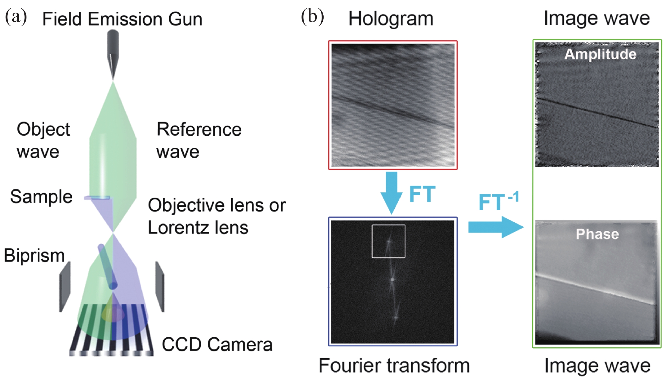
![]()
Figure 1.(Color online) (a) Sketch of off-axis electron holography including three important components: field emission gun, biprism and CCD camera. (b) The reconstruction process of a hologram: The Fourier transform of a hologram produces one center band and two conjugate side bands, one of which is selected and cut out. By applying an inverse Fourier transform, the corresponding amplitude image and phase image can be obtained[
The Fourier transform of the hologram gives one center band and two conjugate sidebands. The separation of the side bands is determined by the voltage applied to the biprism, and the distributed non-periodic intensities around the above spots are caused by electrostatic or magnetic fields in the sample. One of the two side bands is cut out and re-centered. A complex image is obtained by an inverse Fourier transform of the selected side band, and the complex wavefunction can be expressed by:
From which the phase and amplitude can be extracted according to the following formula:
where r and i represent real and imaginary parts of the complex wavefunction, A and ϕ are amplitude and phase of the incident plane wave, μ is a constant relating to beam coherence, microscope stability, and detector properties[
If only electrostatic fields or charge accumulations are involved in the materials, and the electric fringing fields are neglectable close to the sample edges, which are the cases for most semiconductor nanomaterials, the relative phase shift as compared to the reference wave can be expressed by:
where CE is a constant determined by the wavelength of incident electron beam, V is the electrostatic potential including mean inner potential of the material and possible contributions from dopants, band structure engineering or intrinsic polarization fields, z denotes the incident beam direction, and x is specific direction in the plane of specimen. If the sample properties are homogeneous through the thickness of the sample, and there is negligible electrostatic fringing field around the sample, Eq. (4) can be simplified as ϕ(x) = CEV(x)t(x). Here t is the projected sample thickness along the incident electron beam. After the electrostatic potential V is obtained, the corresponding charge density can be calculated by Poisson equation. Thus, in order to obtain quantitative information of electrostatic fields or charge accumulations in semiconductor materials, one needs to ensure that the area of interest is close to vacuum, and accurately determine the projected local sample thickness.
The off-axis electron holography technique has found wide range of applications in semiconductors including semiconductor light-emitting diodes[
3. Charge distributions measurement at the nanometer scale
3.1. Charge distributions of group IV semiconductor nanostructures
Group IV Ge/Si system with type II band alignment has been widely investigated as prominent candidate for device applications. Ge quantum dots (QDs) sandwiched in boron-doped Si are grown by molecular-beam epitaxy (MBE), and electron holography is applied to specific Ge QD to reveal charge distribution and related charge density. The result shows that holes accumulate near the base of the Ge QD. According to revised version of the formula: Vhole = ϕexcess/CEt, the potential produced by accumulated holes can be obtained via the measured excess phase shift ϕexcess. Since the holes are mainly confined under the Ge dot in the wetting layer, the local projected thickness is estimated as the size of the base of the pyramid-shaped Ge dot along the incident electron beam. Based on the obtained electric potential Vhole, the hole density can be calculated by using one-dimensional Poisson equation:
![]()
Figure 2.(Color online) (a, b) Electron hologram and phase image of specific Ge quantum dot sandwiched in Si substrates. The bottom of Ge dot shows extra positive phase shifts indicating holes accumulated in this region[
The epitaxial Ge/Si core/shell nanowires (NWs) oriented along <110> direction are grown on Si (111) substrate by chemical vapor deposition (CVD) following the vapor-liquid-solid growth mode. Electron holograms and high-angle annular-dark-field (HAADF) STEM images are obtained from individual NWs. While the HAADF images provide accurate information of the projected thicknesses of the Ge and Si regions for the selected core/shell NW based on the fact the HAADF intensity is proportional to the projected thickness of the sample ( Figs. 2(c) and 2(d)), quantitative electron holography characterization of the same NW indicates that holes are selectively distributed in the Ge core as extra positive phase shifts appear in the Ge core region (Figs. 2(e) and 2(f)). The corresponding hole density is about 0.4 ± 0.2 nm–3, which is one order of magnitude higher than that for Ge QDs, which proves the better charge confinement capability of one-dimensional NWs as compared to zero-dimensional QDs[
For in-situ electron holographic study of group IV semiconductor nanostructures, Gan et al. report the electrical properties of axial Si-Ge NW heterojunctions characterized by electron holography and atom-probe tomography (APT). While the APT measurement provides total dopant concentration profiles for B, P, and the unintentional dopant Ga, the quantitative characterization by electron holography reveals that the built-in potential offset is about 0.5 ± 0.6 V with the Ge side lower. Further in-situ biasing experiment combined with electron holography indicates that when the Si side is positively biased, the built-in potential increases with biasing voltages; when the Si side is negatively biased, the built-in potential is not much affected, as presented in Figs. 3(a)–3(e)[
![]()
Figure 3.(Color online) (a, b) TEM image of an axially biased Si–Ge nanowire heterojunction, and the Ge side is grounded. (b) Electron hologram of the nanowire with +3 V bias on the Si side. (c) Corresponding phase image. (d) Potential line profile of the region indicated by a white arrow in (c), which show abrupt changes at positive bias, and comparatively much less variations at negative bias. (e) Corresponding
Meanwhile, by combining in situ TEM holder for lithiation and electron holography technique, Gan et al. quantitatively characterizes the dynamic process of lithium ion insertion into Ge NWs. It is found that the Ge NW would turn into Ge/LixGe core/shell structure with increasing shell thickness during the lithiation process. As sketched in Fig. 3(f), the surface of Ge core is negatively charged, leading to lower mean inner potential of the Ge core as compared to theoretical values. On the other hand, the inner surface of the LixGe shell would be positively charged to maintain charge balance, and the remainder of the metallic LixGe shell is free of net charge. According to Fig. 3(g), the calculated phase shift profile based on this charge distribution model fits well to experimental data, which confirms the validation of the proposed charge distribution model[
3.2. Charge distributions of compound semiconductor nanostructures
The combination of zero-dimensional QDs and one-dimensional NWs show great prospects in various optoelectronic devices. InAs QDs decorating GaAs NWs are grown via metal-organic chemical vapor deposition (MOCVD). A polarization effect is clearly demonstrated at nanometer scale by electron holography: the n-type doped InAs QDs show large amount of free electrons accumulated at the dots apexes, while the GaAs NW core would accumulate holes to satisfy charge neutralization. As a result, a radial polarization field would form, which leads to changes in the band structure of the hybrid QDs/NW system, and allows more electron-hole recombinations in the QD regions. These results explain well the observed enhanced photoluminescence (PL) intensity after introducing InAs QDs to the GaAs NW surface (Figs. 4(a)–4(d))[
![]()
Figure 4.(Color online) (a) Charge distribution profile across InAs QD decorating GaAs NW hetero-interfaces obtained from holographic reconstruction of the phase shifts across the InAs QD/GaAs NW interface. (b) Band structure induced charge redistribution of InAs QDs/GaAs NW heterostructures, which confirms accumulation of electrons at the dot apex and charges of opposite signs distributed at the hetero-interface. (c, d) PL spectra of InAs QDs/GaAs NW (red) and pure GaAs NW (black) for comparison[
The embedded radial quantum wells (QWs) in semiconductor NWs would allow confined electronic states along radial direction and free movements along the growth direction of the NWs. Here, radial GaAs QWs (~ 6.6 nm in width) are embedded in AlGaAs NWs with nearly perfect lattice matching. According to the electron holographic results at Al0.4Ga0.6As/GaAs QW/Al0.2Ga0.8As heterostructures: a large number of electrons accumulate in the GaAs QW, and considerable holes distribute at GaAs/AlGaAs interfaces, which causes band bending at these interfaces (Figs. 4(e) and 4(f)). Density functional theory (DFT) calculations reveal that the introduction of GaAs QW would lead to quantum confinement effect in this heterostructure, and the resultant changes in band gap explains well the observed blue-shift of the GaAs QW peak as compared to that of single GaAs NW in the corresponding PL spectra[
The configurations of QDs decorating NWs and core/shell NWs are combined forming InAs QDs decorating GaAs/AlAs core/shell NWs, which is expected to bring more benefits to applications in photoelectric devices. Quantitative characterizations by electron holography show considerable electrons distributing in the InAs QD apex region. Charges of reversed signs and close densities distribute at sequential interfaces due to type-I band alignment and energy band bending at the interfaces. Holes would distribute in NW core to maintain overall charge neutralization. The AlAs buffer layer would help adjust band structures of the hetero-interfaces with improved confinement of electrons, and facilitate InAs QDs growth on GaAs NWs with enhanced stability[
III-nitride semiconductor nanostructures have direct band gap, flexible band structure engineering, and strong polarization-related internal electric fields, which are promising for single-NW devices. GaN/AlN heterostructural NWs grown by plasma-assisted molecular-beam epitaxy are quantitatively studied by electron holography. The obtained potential profile shows obvious deviation of the AlN top region as compared to simulations, which could be attributed to positive charging of the NW under electron beam irradiation[
Serial research on GaN NWs by in-situ electron holography reveals that the width of the space charge (SC) layer is about 76 nm at static state, and varies between 68 and 91 nm corresponding to the saturated states under forward and reverse bias conditions, respectively. Based on the above measurements, the donor density of GaN NWs is estimated to be about 4.3 × 106 cm–3[
![]()
Figure 5.(Color online) (a) TEM image of specific straight GaN nanowire connected between two Au electrodes forming a closed electrical circuit. (b) Phase image of the straight GaN nanowire close to the M–S junction. (c) Phase shift line profile of the region labeled by a red line in (b), and the red line indicates average values of the phase shift profile. (d) TEM image of a bent GaN nanowire connected between two Au electrodes. (e) Phase image of the bent GaN nanowire at the M–S junction showing different phase contrasts along radial direction. (f) Phase shift line profiles along the red and green arrows, respectively. The red and green lines represent their average values[
Besides the above group III–V compound semiconductor nanostructures, group II–VI NWs as well as group II–VI/group III–V heterostructural light emitting diode (LED) device are also quantitatively studied at nanometer scale. The depletion length as a function of reverse bias voltage for ZnO NW with a Schottky contact is first measured by cathodoluminescence and voltage contrast experiments. As presented in Fig. 6(a), electron holography characterizations combined with electrical in-situ biasing are carried out for comparison. Meanwhile, 3D calculations of the depletion width W using the Nextnano3 software are carried out (Fig. 6(b)), and the results indicate an active core diameter of 70–75 nm with an n-type doing level of 1018 cm–3, and negative surface charges of density 2.5 × 1012 cm–2, leaving a depleted surface region of around 36 nm, which is consistent with three-dimensional simulations[
![]()
Figure 6.(Color online) (a) Potential profiles at –5, –10 and –15 V bias, respectively. The inset shows corresponding phase image. The solid arrow labels the nanowire core for phase profiling, and the two dotted arrows indicate the vacuum regions on either side of the nanowire for phase profiling. (b) 3D calculations of the depletion width W using the Nextnano3 software. The selection of doping level
Non-polar a-plane n-ZnO/p-AlGaN and n-ZnO/i-ZnO/p-AlGaN heterojunction film LEDs are synthesized by MOCVD. Performance enhancement is clearly observed for the LED device by introducing the i-ZnO layer. Comprehensive structural characterizations indicate smaller ratio of lattice mismatch and lower strain level in the p–i–n heterojunction as compared to p–n heterojunction. Based on the reconstructed electron holographic results of the two types of LED heterostructures (Figs. 6(c)–6(f)), the introduced i-ZnO layer corresponds to a region with flat electrostatic potentials, which offers more chances for carrier movements, enhanced possibilities of exciton recombination, and ensures prominent electroluminescence properties[
3.3. Charge distributions of two-dimensional semiconductor nanostructures
The two dimensional (2D)/2D MXene/MoS2 heterostructure is expected to show excellent microwave absorption performance. However, the synergistic effect of the two types of 2D material is still ambiguous. The MXene/MoS2 composites are synthesized by hydrothermal reaction, and quantitatively analyzed by electron holography. The color change in the charge density map indicates overlap of MoS2 nanosheets in local regions. In the charge density profile, the upward peaks correspond to accumulation of positive charges, and the downward peaks indicate distribution of negative charges, which would lead to strong interfacial polarization, as shown in Figs. 7(a)–7(d). Since charge accumulation often take place at the interfaces, and the MoS2 nanosheets confined among multi-layered MXene would form large amount of 2D/2D heterostructural interfaces, the resultant strong interfacial polarization would highly enhance the microwave absorption performance[
![]()
Figure 7.(Color online) (a) Electron hologram of MXene-MoS2 2D/2D heterostructure. (b) Corresponding charge density image. (c, d) Charge density line profiles corresponding to the white arrows labeled as (e) and (f), respectively[
Similar method is also applied to MoS2/FeS2 heterojunction. Small FeS2 nanopieces are grown on the surface of MoS2 flakes by a facial hydrothermal method. The resultant charge density map and electric field map show obvious fluctuations. The charge density profile across the FeS2 pieces indicates positive charges gathered on one side, and negative charges accumulated on the other side of the MoS2/FeS2 interface forming local polarized field, as presented in Figs. 7(e)–7(h). The abundant charges distributed at the interface would capture and convert the incoming electromagnetic wave energy into kinetic energy until resonance is achieved. Meanwhile, the strong polarized field (around 0.027 V/nm) would facilitate formation of local stray electric fields with multiple directions. The intrinsic dipole moment and the multi-directional stray electric field would be re-oriented along similar directions when they are excited by the propagating electromagnetic wave, which would form macroscopic polarization effect and consume the energy of incoming electromagnetic wave. Although there is currently no actual application, these local layered heterojunctions would facilitate the fabrication of highly efficient microwave absorption devices in the near future[
4. Conclusion
In this review, the structure-property relationships of various semiconductor nanostructures are quantitatively studied by off-axis electron holography technique, which can provide nanoscale electrostatic potentials, electric fields and charges at the interfaces of the hetero-structural semiconducting materials. The applications of off-axis electron holography to group IV, compound, and two-dimensional semiconductor nanostructures are systematically presented, focusing on the extraction of charge distributions at the hetero-interfaces and the underlying structure-property relationships.
Although off-axis electron holography is powerful in characterizing phase shift and related electrostatic properties in semiconductor nanostructures, some challenges and concerns still exist about the sample under study: firstly, the area of interest needs to be very close to vacuum, or the secondary image would overlap with the original one, making the phase reconstruction process almost impossible. If the area of interest is not so close to vacuum, we could make an indentation in the neighborhood by focused ion beam to deliberately introduce the vacuum region close to where we’re interested. Secondly, samples of poor conductivity are not suitable for electron holography analysis, since the incident electrons would accumulate on the sample surface forming strong fringing field, which would mess up the intrinsic electrostatic field that really matters. Coating a thin layer of carbon would alleviate this situation to some extent. Thirdly, the presence of native oxide on the sample surface and inactive dopants within the semiconducting material would also complicate the quantitative characterization of electrostatic fields since they would have different contributions to the overall phase shifts from that of the active dopants. To deal with this issue, one could clear the sample surface at low angles by low energy Ar ions as much as possible, and combine device simulations to determine the level of inactive dopants. Moreover, the application of in situ electrical biasing would be other choice, which could determine the changes in depletion width and built-in potential as functions of the applied bias[
While the static structural determinations have been successfully realized at atomic resolution thanks to the high brightness of the field emission gun with highly coherent current, the spherical aberration (Cs) corrector and monochromator with greatly improved information limit, it becomes also possible to quantify extreme small electrostatic fields and relate them with the crystal structures at atomic resolution by aberration-corrected electron holography[
Meanwhile, real-time observations are always the short slab of off-axis electron holography since it usually requires off-line processing. The development of faster computer system and rapid imaging system would make the near-real-time phase reconstruction possible in the near future. With technical improvement in the in-situ sample holders, the quantitative characterizations of electric properties of semiconductor nanostructures under various stimuli by in-situ electron holography are largely reported, making evaluation of nanometer scale electric properties of semiconductor devices at their working conditions possible. However, obtaining quantitative electric properties at working conditions contains some complex issues. For example, the electric potential profile of reverse biased GaN-based LED is quite noisy as the fringes are prone to be deteriorated by electromagnetic interference[
Acknowledgements
This work was supported by the National Natural Science Foundation of China (51871104), the Fundamental Research Funds for the Central Universities (No. 2019kfyRCPY074). L. Y. L. thanks Prof. David Smith, Prof. Martha McCartney, Prof. Jiangnan Dai, Prof. Xin Yan for their great support in related work.
References
[1] M M Waldrop. The chips are down for Moore's law. Nature, 530, 144(2016).
[2] L Li, Z Gan, M R McCartney et al. Atomic configurations at InAs partial dislocation cores associated with Z-shape faulted dipoles. Sci Rep, 3, 3229(2013).
[3] L Li, F Tu, L Jin et al. Polarity continuation and frustration in ZnSe nanospirals. Sci Rep, 4, 7447(2014).
[4] D J Smith. Atomic-resolution structure imaging of defects and interfaces in compound semiconductors. Prog Cryst Growth Charact Mater, 66, 100498(2020).
[5] W L Bragg. Microscopy by reconstructed wave-fronts. Nature, 166, 399(1950).
[6] A V Crewe, M Isaacson, D Johnson. A simple scanning electron microscope. Rev Sci Instrum, 40, 241(1969).
[7] J M Cowley. Twenty forms of electron holography. Ultramicroscopy, 41, 335(1992).
[8] L Y Li, X K Hu, Y H Gao. Electron holographic study of semiconductor light-emitting diodes. Small, 14, 1701996(2018).
[9] H Lichte, P Formanek, A Lenk et al. Electron holography: Applications to materials questions. Annu Rev Mater Res, 37, 539(2007).
[10] M R McCartney, M Gajdardziska-Josifovska. Absolute measurement of normalized thickness,
[11] M A Gribelyuk, M R McCartney, J Li et al. Mapping of electrostatic potential in deep submicron CMOS devices by electron holography. Phys Rev Lett, 89, 025502(2002).
[12] M I den Hertog, H Schmid, D Cooper et al. Mapping active dopants in single silicon nanowires using off-axis electron holography. Nano Lett, 9, 3837(2009).
[13] L Y Li, D J Smith, E Dailey et al. Observation of hole accumulation in Ge/Si core/shell nanowires using off-axis electron holography. Nano Lett, 11, 493(2011).
[14] Z F Gan, M Gu, J S Tang et al. Direct mapping of charge distribution during lithiation of Ge nanowires using off-axis electron holography. Nano Lett, 16, 3748(2016).
[15] L Zhou, D J Smith, M R McCartney et al. Measurement of electric field across individual wurtzite GaN quantum dots using electron holography. Appl Phys Lett, 99, 101905(2011).
[16] M R McCartney, R E Dunin-Borkowski, D J Smith. Quantitative measurement of nanoscale electrostatic potentials and charges using off-axis electron holography: Developments and opportunities. Ultramicroscopy, 203, 105(2019).
[17] F Kern, M Linck, D Wolf et al. Autocorrected off-axis holography of two-dimensional materials. Phys Rev Res, 2, 043360(2020).
[18] L Y Li, S Ketharanathan, J Drucker et al. Study of hole accumulation in individual germanium quantum dots in p-type silicon by off-axis electron holography. Appl Phys Lett, 94, 232108(2009).
[19] Z F Gan, D E Perea, J Yoo et al. Characterization of electrical properties in axial Si-Ge nanowire heterojunctions using off-axis electron holography and atom-probe tomography. J Appl Phys, 120, 104301(2016).
[20] F Cheng, B Li, L Y Li et al. Study of the polarization effect in InAs quantum dots/GaAs nanowires. J Phys Chem C, 123, 4228(2019).
[21] C Li, Y F Cheng, B Li et al. Study of charge distributions and electrical properties in GaAs/AlGaAs single quantum well/nanowire heterostructures. J Phys Chem C, 123, 26888(2019).
[22] T Y Qi, Y F Cheng, F Cheng et al. Study of nanometer-scale structures and electrostatic properties of InAs quantum dots decorating GaAs/AlAs core/shell nanowires. Nanotechnology, 31, 245701(2020).
[23] M den Hertog, R Songmuang, E Monroy. Polarization fields in GaN/AlN nanowire heterostructures studied by off-axis holography. J Phys: Conf Ser, 471, 012019(2013).
[24] X Chen, Y G Wang, J Guo et al.
[25] X Chen, Y G Wang, J K Jian et al. Effect of strain on space charge layer in GaN nanowires investigated by
[26] X Chen, Y G Wang, J K Jian et al. Controlling charges distribution at the surface of a single GaN nanowire by
[27] M den Hertog, F Donatini, R McLeod et al.
[28] F Jiang, J W Chen, H Bi et al. The underlying micro-mechanism of performance enhancement of non-polar n-ZnO/p-AlGaN ultraviolet light emitting diode with i-ZnO inserted layer. Appl Phys Lett, 112, 033505(2018).
[29] X Li, C Y Wen, L T Yang et al. Enhanced visualizing charge distribution of 2D/2D MXene/MoS2 heterostructure for excellent microwave absorption performance. J Alloys Compd, 869, 159365(2021).
[30] L S Xing, X Li, Z C Wu et al. 3D hierarchical local heterojunction of MoS2/FeS2 for enhanced microwave absorption. Chem Eng J, 379, 122241(2020).
[31] T Kawasaki, Y Takahashi, T Tanigaki. Holography: application to high-resolution imaging. Microscopy, 70, 39(2020).
[32] D Wolf, A Lubk, P Prete et al. 3D mapping of nanoscale electric potentials in semiconductor structures using electron-holographic tomography. J Phys D, 49, 364004(2016).
[33] L Z Y Liu, C McAleese, D V Sridhara Rao et al. Electron holography of an
[34] S Yazdi, T Kasama, M Beleggia et al. Towards quantitative electrostatic potential mapping of working semiconductor devices using off-axis electron holography. Ultramicroscopy, 152, 10(2015).

Set citation alerts for the article
Please enter your email address
© Copyright 2018-2021 | Chinese Laser Press. All Rights Reserved 沪ICP备15018463号-20