• Journal of Semiconductors
  • Vol. 43, Issue 5, 051201 (2022)
Wei Wen1、2, Yunlong Guo1、2, and Yunqi Liu1、2
Author Affiliations
  • 1Institute of Chemistry, Chinese Academy of Sciences, Beijing 100190, China
  • 2University of Chinese Academy of Sciences, Beijing 100049, China
  • show less
    DOI: 10.1088/1674-4926/43/5/051201 Cite this Article
    Wei Wen, Yunlong Guo, Yunqi Liu. Multifunctional neurosynaptic devices for human perception systems[J]. Journal of Semiconductors, 2022, 43(5): 051201 Copy Citation Text show less

    Abstract

    The traditional Von Neumann architecture for processing information is difficult to meet the needs of the big data era, while low-power, small-sized neurosynaptic devices can operate and store information, so that they have received extensive attention. Due to the development of artificial intelligence and robotics, neurosynaptic devices have been given high expectations and requirements. The trend of functionalization, intelligence, and integration of computing and storage is obvious. In this review, the basic principles and types of neurosynaptic devices are summarized, the achievements of neurosynaptic devices for human perception systems are discussed and a prospect on the development trend is also given.

    1. Introduction

    With the advent of the big data era, computers store and calculate information with explosive growth, which will inevitably lead to the need for computers to increase their scales and invest more hardware devices at the current level of computing. Most computers today are still designed according to the architecture of "programmed storage, sharing data, sequential execution" proposed by Von Neumann[1]. However, due to the inefficient use of computational resources, people must rely on the help of supercomputers when performing large-scale data operations. Its shortages of large power consumption and floorspace are becoming more prominent in the era of data explosion. In contrast, the human brain is only about 1.5 kg with the volume of about 1200 cm3, but has 1016 neurons, which can process about 86 million pieces of information in one day with only about 20 W consumption[2-4]. Therefore, people’s attention is directed to the research of neurosynaptic devices. By imitating the information processing function of synapses, the devices with small size and low power consumption provide a favorable premise for simulating the extremely large and complex perception systems of human beings[5]. The human perception comes from vision, touch, hearing, taste and smell, corresponding to a visual system, somatosensory system, auditory system, gustatory system and olfactory system, respectively. Each perception system provides our brains with rich information all the time. This process requires the cooperation of thousands of neurons, while synapses are the crucial part to transmit information among neurons.

    In recent years, scholars have modified existing physical devices based on their understanding of the structure and the function of nerve synapses, and derived a series of neurosynaptic devices with different structures and mechanisms. With the application of massive optoelectronic materials, ionic liquids, ferroelectric materials, flexible materials, etc. to neurosynaptic devices, the development of this field gradually becomes multifunctional, diversified, intelligent, and biomimetic. Therefore, scholars have put forward higher requirements for stability, biocompatibility, flexibility, low power consumption and other performance characteristics. Nowadays, neurosynaptic devices have not been limited to imitate basic synaptic functions, but expanded to the aspects of mechanisms, materials, device structures, integration and applications. Although numerous literature has made comprehensive, timely and constructive summaries on the development of neurosynaptic devices, few scholars have noticed the important role played by neurosynaptic devices in simulating the human perception systems and the significant achievements that have been made. Hence, this article will focus on the introduction and summary of this field, hoping to arouse scholars' attention and interest. In order to describe neurosynaptic devices clearly, the basic principles and device types of neurosynaptic devices are systematically introduced before discussing the imitation of the human perception systems. Finally, a summary and a critical evaluation are also given based on our comprehension of this field.

    2. Neurosynaptic devices

    Before using physical devices to simulate synapses, the devices first need to achieve synaptic plasticity functionally. Synaptic plasticity describes the phenomenon that the effectiveness of synaptic information transmission among neurons increases or decreases with changes in their neural activities. The “synaptic weight” is used to measure the strength of signal transmission between synapses. Synaptic plasticity includes short-term plasticity (STP), long-term plasticity (LTP), spiking-timing-dependent plasticity (STDP), and spiking-rate-dependent plasticity (SRDP) etc.[6]. Short-term plasticity is achieved by temporarily strengthening synaptic connections, often lasting tens of milliseconds to a few minutes and then returning to the initial state. Short-term plasticity is considered to play an important role in neural signal transmission and information processing[7]. According to the different behaviors of stimuli on synapses, it is often divided into paired-pulse facilitation (PPF), paired-pulse depression (PPD), and post-tetanic potentiation (PTP). However, repeated stimuli will cause the synaptic weight to change permanently, thereby realizing the transition from short-term plasticity to long-term plasticity. Reducing the time interval of impulses and increasing the duration or intensity of impulses can effectively achieve long-term plasticity. This process is very similar to the repetitive learning and memory behaviors of humans. Long-term plasticity can be divided into long-term potentiation (LTP) and long-term depression (LTD). Spiking-timing-dependent plasticity means that the different time sequences of pre-synaptic pulses and post-synaptic pulses lead to the enhancement or weakening of synaptic actions. Spiking-rate-dependent plasticity reflects the influence of synaptic activity frequency on synaptic plasticity, the symbol and value of synaptic plasticity are determined by the frequency of the presynaptic pulse. Both STDP and SRDP are important mechanisms in the process of biological learning and memory[6]. For neurosynaptic devices, controllable, continuous and linear modulating the conductance or resistance of devices is the prerequisite for simulating nerve synapses to achieve excitation and inhibition of signal transmission by adjusting synaptic weights. In 2008, Hewlett-Packard Company (HP) developed the first memristor with tunable resistance and memory characteristics, which promoted the invention of new mechanisms and new structures of neuromorphic devices[8]. At present, two-terminal memristors and three-terminal transistors are the hotspots in the research area of neurosynaptic devices.

    2.1. Two-terminal memristors

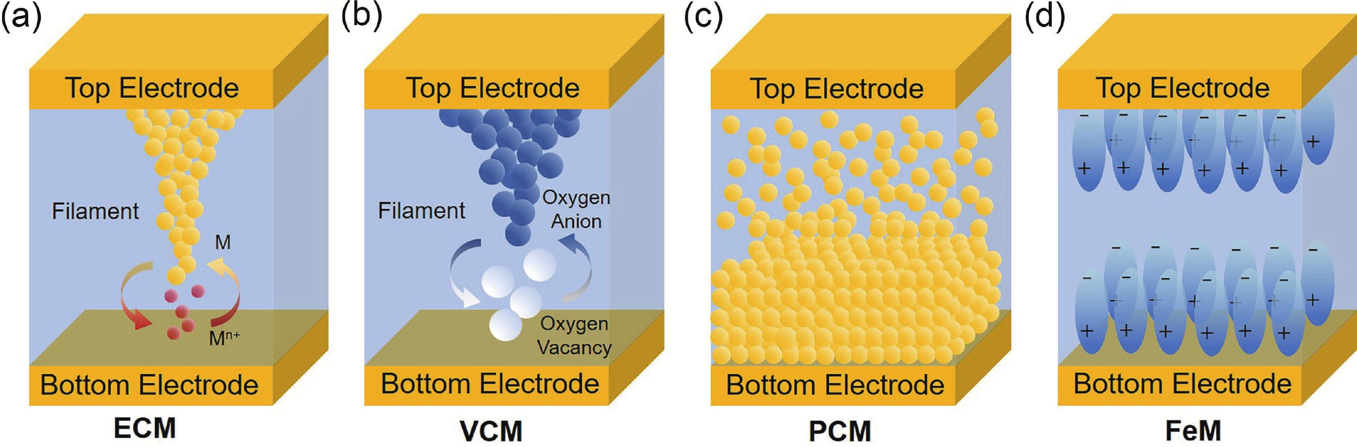
    Due to the simple structure, memristors are easy to integrate on a large scale with a low cost. The memristor is generally composed of a top electrode, a resistive change layer, and a bottom electrode stacked on top of each other. The top electrode can be regarded as the presynaptic membrane, while the bottom electrode serves as the postsynaptic membrane. Synaptic response is achieved by adjusting the conductance between the two electrodes. The working mechanisms of memristors are usually divided into four types as follows: electrochemical metallization mechanism (ECM), valence change mechanism (VCM), and phase change mechanism (PCM) and ferroelectric mechanism (FeM), as illustrated in Fig. 1.

    (Color online) The working mechanisms of two-terminal memristors. (a) Electrochemical metallization mechanism. (b) Valence change mechanism. (c) Phase change mechanism. (d) Ferroelectric mechanism.

    Figure 1.(Color online) The working mechanisms of two-terminal memristors. (a) Electrochemical metallization mechanism. (b) Valence change mechanism. (c) Phase change mechanism. (d) Ferroelectric mechanism.

    Electrochemical metallization mechanism: When a positive voltage is applied to the electrode of the device, the metal electrode loses electrons at the anode in the oxidation reaction. The metal ions migrate to the cathode under the force of the electric field and are reduced to elemental metals again after obtaining electrons. As a result, the elemental metals gradually accumulate to form conductive filaments[9]. Hence, the device switches from a high resistance state to a low resistance state. In contrast, when the direction of the electric field is reversed, the oxidation-reduction reactions and the cation migration process facilitate the rupture of conductive filaments, causing the device to switch back to the high-resistance state.

    Valence state transition mechanism: Resistance switching phenomena are often observed in some transition metal oxides. When a positive voltage is applied to the positive terminal of the device, the oxygen vacancies in the materials migrate under the electric field force. In the meantime, a local electrochemical oxidation-reduction reaction similar to the electrochemical metallization mechanism occurs at two electrodes[10]. Since the resistance of the region rich in oxygen vacancies is low and that of the region lacking oxygen vacancies is high, the oxygen vacancies form conductive channels during the migration process. In contrast, if a negative voltage is applied to the positive terminal, the resistance of the device will increase due to the rupture of the conductive channels. The memristors realize the regulation of the resistance based on the migration of oxygen vacancies and redox reactions.

    Phase transition mechanism: When the current is passed, the generation and accumulation of Joule heat induces the temperature of metals over the melting point. With a rapid cooling process, the metals undergo a reversible phase transition from crystalline to amorphous. Conversely, low-voltage pulses crystallize the phase change material[11]. Because the resistance of crystalline and amorphous metals is significantly different, the current changes obviously before and after the phase transition. Hence, the mechanism makes it possible to control the conductivity of memristors by using programmed voltages.

    Ferroelectric mechanism: The behavior of spontaneous polarization induced by the external electric field can be commonly found in ferroelectric materials, which causes the resistance of the device to change. Since this phenomenon has been initially used on ferroelectric random-access memories (FeRAM)[12], ferroelectric memristors have potential applications in neuromorphic computing systems.

    2.2. Three-terminal synaptic transistors

    A three-terminal synaptic transistor is usually composed of a semiconductor layer, a gate dielectric layer and a source/drain/gate electrode. The gate electrode and the conductive channel are regarded as the presynaptic terminal and the postsynaptic membrane, respectively. The synaptic signals of three-terminal synaptic devices can modulate the synaptic weight through the independent gate electrode. Since the transistor has one more electrode than the memristor, the transistor can more effectively realize the simulation of biological synapses and provide more synaptic functions and applications. At present, three-terminal synaptic transistors can be roughly divided into floating-gate transistors (FGTs), electrolyte-gate transistors (EGTs), ferroelectric field-effect transistors (FeFETs) and optoelectronic synaptic transistors (OSTs) according to their working mechanisms[13], as illustrated in Fig. 2.

    (Color online) The types of three-terminal synaptic transistors. (a) Floating-gate transistors. (b) Electrolyte-gate transistors. (c) Ferroelectric field-effect transistors. (d) Optoelectronic synaptic transistors.

    Figure 2.(Color online) The types of three-terminal synaptic transistors. (a) Floating-gate transistors. (b) Electrolyte-gate transistors. (c) Ferroelectric field-effect transistors. (d) Optoelectronic synaptic transistors.

    A floating gate transistor is composed of a gate electrode, a blocking oxide layer, a floating gate layer, a tunneling oxide layer, a semiconductor layer, a source electrode and a drain electrode. When the gate voltage is applied, charges are easily injected into the floating gate through thermal excitation or quantum tunneling[14, 15], and are stored in the floating gate layer due to the existence of the charge blocking layer and the tunneling layer. The pulse voltage applied to the gate can effectively modulate the number of charges trapped in the floating gate, resulting in a shift of the threshold voltage, thereby changing the channel conductance and realizing the modulation of the synaptic weight. Floating gate transistors have the advantages of large charge storage capacity, stable and easily modulated channel conductance, and large switching ratio. However, researchers need to overcome its high operating voltage and solve the shortage that short-term plasticity and long-term plasticity is difficult to achieve in one transistor at the same time[13]. Floating gate transistors often use thin metal layers or organic conductive polymer films as floating gate layers. But due to lateral leakage, the charge retention capability of the film is poor[14]. Therefore, there are increasingly reports of fullerene nanoparticles[15], gold nanoparticles[16-18], silver nanoparticles[19, 20], and perovskite quantum dots[21] as floating gate layers in recent years. Studies have found that nanoparticle floating gate transistors have better transconductance gain. Adjustable size and morphology of nanoparticles can effectively change the synaptic behavior of the transistors[13]. Perhaps nanoparticle floating-gate transistors will become the trend of floating gate synaptic transistors development in the future.

    The electrolyte gate transistor is composed of a source electrode, a drain electrode, an electrolyte dielectric layer, a semiconductor layer and a gate electrode. Electrolyte gate transistors use the ions in the electrolyte dielectric layer to adjust the channel conductance of the device and achieve synaptic weight modulation as well. The working principle of electrolyte gate transistors can be simply divided into two types: electrostatic modulation and electrochemical doping[22], corresponding to electric double-layer transistors and electrochemical transistors, respectively. For electric double-layer transistors, under the applied electric field, the ions in the electrolyte move and gather at the interface between the semiconductor layer and the dielectric layer, resulting in the formation of an electric double layer with high capacitance around the interface. The electric double layer affects the electric field applied by the gate, therefore changing the channel conductance. For electrochemical transistors, ions in the electrolyte can penetrate into the semiconductor layer, further doping and modulating the channel conductance in a non-volatile manner. The migration of ions in the electrolyte is very similar to the releasing process of neurotransmitters. The gate electrode of an electrochemical transistor can be regarded as a presynaptic membrane, while the semiconductor channel is regarded as a postsynaptic membrane, and the channel conductance can be regarded as the synaptic weight. When the electrochemical transistor works in the electrostatic modulation state, the change of channel conductance is reversible, which provides a basis for simulating short-term plasticity; when it works in the electrochemical doping mode, the ions are doped to the channel causing irreversible change in channel conductance, which leads to long-term plasticity[13]. Moreover, electrolyte transistors have a lower operating voltage, which provides the possibility for the realization of ultra-low energy synaptic devices[23].

    The ferroelectric field-effect transistor is composed of a source electrode, a drain electrode, a semiconductor layer, a ferroelectric dielectric layer, and a gate electrode. The ferroelectric dielectric layer is the key to realize the synaptic function of the transistor. The ferroelectric materials have a spontaneous polarization state, and the carrier concentration of the ferroelectric field-effect transistors is precisely modulated by gate voltage to change the polarization state of the ferroelectric materials. The ferroelectric insulators switch between the two remnant polarization states, corresponding to the two digital states of the memory: “0” and “1”. The ferroelectric field-effect transistors have the advantages of multi-level conductance, large on-off ratio, high stability, lossless readout, low power consumption, high operating speed, small device size and simple manufacturing process[24]. However, high operating voltage, high crystallization temperature and rigidity of ferrites limit the application of ferroelectric field-effect transistors in large-area synaptic arrays and flexible devices, etc. Fortunately, the introduction of organic ferroelectrics represented by poly(vinylidene fluoride-trifluoroethylene) (P(VDF-TrFE)) has brought vitality to the development of ferroelectric field-effect transistors[25].

    The difference between the optoelectronic synaptic transistor and the synaptic devices described above is that it introduces light as another effective way to modulate the channel conductance besides the gate. Because light can provide synaptic devices with large bandwidth, low interconnection energy loss and ultra-fast signal transmission, optoelectronic synaptic transistors have become one of the most popular research directions for synaptic devices[26-28]. The working mechanism of the optoelectronic synaptic transistor can be mainly attributed to the capture of photo-generated carriers. When light reaches the interface between the semiconductor layer and the dielectric layer, photogenerated electron–hole pairs are separated at the interface, and some electrons or holes will be trapped at the interface or in the dielectric layer, thereby producing the photon memory effect[6]. In addition, the device needs enough negative gate voltage pulses to completely erase the memory effect. Although optoelectronic synaptic devices can control conductance through light in real time to achieve functions that other synaptic devices cannot achieve, it is still a big challenge for optoelectronic synaptic devices to use pure optical signals to achieve inhibitory synaptic properties. Nevertheless, optoelectronic synaptic devices are valued continuously by scholars.

    After nearly a decade of development, neurosynaptic devices are no longer simply satisfied with simulating synaptic plasticity. The advent of artificial intelligence, the internet of things, big data, and the era of bionic robots has put forward higher requirements for neurosynaptic devices. Massive functional materials and the innovation of device structures provide preconditions for the systematization, functionalization and intelligence of neurosynaptic devices. Moreover, neurosynaptic devices at present can achieve rapid response to various external stimuli such as light signals and electrical signals, which greatly expands the range of applications of neurosynaptic devices. Because the process of neurosynaptic devices responding to external stimuli is very similar to that of humans feeling the external world, neurosynaptic devices can effectively shape and imitate the human perception systems. Therefore, this review will summarize the achievements of the imitation of human perception systems from five parts: the visual system, the somatosensory system, the auditory system, the gustatory system and the olfactory system.

    3. The imitation of human perception systems

    3.1. Visual system

    Among the information received by humans, more than 80% comes from the visual sense organs[29, 30]. The human eye is constantly processing information about the color, shape, movement and position of objects, efficiently converting light signals received by the retina into electrical signals, which are sent to the central nervous system for information analysis and processing. The human visual system has many optic neurons with synapses. They can not only detect image information, but also store data. Therefore, they can process a large amount of information in parallel, and each synapse activity consumes only 1–100 fJ. Hence, the integration of image sensing, storage and processing functions into a single space of the device with real-time processing and calculation of image signals are of great significance to the realization of artificial neuromorphic vision systems[31]. It is one of the most feasible strategies for artificial neuromorphic visual systems to construct optoelectronic synaptic devices and realize visual processing functions through analog electronic circuits.

    Optoelectronic synaptic devices have the advantages of both optoelectronic sensors and synaptic devices. Synaptic devices process, amplify and store the information of light intensity, color and frequency obtained by the optoelectronic sensor in real time[32]. The optoelectronic synaptic device can be realized by a two-terminal memristor or a three-terminal synaptic transistor. It can also be fabricated simply by the integration of an optoelectronic sensor and a synaptic device.

    Sun et al.[33] utilized CsPbBr3 perovskite quantum dots with excellent optical properties to construct a flexible ultra-sensitive array in which P-type carbon nanotubes serve as conductive channels, as illustrated in Fig. 3. N-type quantum dots and P-type carbon nanotubes form a P–N junction. Light generates excitons at the P–N junction and the quantum dots capture electrons at the interface, making neurosynaptic function and light responsivity possible. The 1024-pixel flexible optoelectronic synaptic transistor array has great light sensitivity and stability. When the light energy density is 0.01 μW/cm2, the device responsivity reaches the maximum as 5.1 × 10⁷ A/W, and the external quantum efficiency can reach 1.6 × 10¹⁰%, the normalized detection degree can reach up to 2 × 10¹⁶ Jones, which is the highest level of optoelectronic synaptic devices of its kind published. In addition, synaptic arrays exhibit the properties of short-term plasticity, long-term plasticity and paired-pulse facilitation, which can realize image information response and storage. After 200 times of repeated learning, the device array can recognize and memorize human images, which has an important role and significance for realizing the simulation of the artificial visual system.

    (Color online) (a) Schematic diagram of phototransistor structure. (b) Schematic diagram of the heterojunction band before and after light. (c) Sensor array chip, wires bonding on printed circuit board (scale bar: 5mm). (d) Optical micrograph of 32 × 32 sensor array (scale bar: 500μm). (e) Measured training weight results of a number 8 pattern in the initial state and after training under 405 nm light with a lighting power density of 1 μW/cm2 (pulse width, 250 ms; pulse interval, 250 ms). (f) Measured training weight results of the sensor array after training with 10 pulses under a 405 nm light with various lighting power densities (pulse width, 250 ms; pulse interval, 250 ms). (g) Simulation results of a man’s face in the initial state and after training processes. Reproduced with permission[33]. Copyright 2021, Springer Nature.

    Figure 3.(Color online) (a) Schematic diagram of phototransistor structure. (b) Schematic diagram of the heterojunction band before and after light. (c) Sensor array chip, wires bonding on printed circuit board (scale bar: 5mm). (d) Optical micrograph of 32 × 32 sensor array (scale bar: 500μm). (e) Measured training weight results of a number 8 pattern in the initial state and after training under 405 nm light with a lighting power density of 1 μW/cm2 (pulse width, 250 ms; pulse interval, 250 ms). (f) Measured training weight results of the sensor array after training with 10 pulses under a 405 nm light with various lighting power densities (pulse width, 250 ms; pulse interval, 250 ms). (g) Simulation results of a man’s face in the initial state and after training processes. Reproduced with permission[33]. Copyright 2021, Springer Nature.

    Chen et al.[32] connected an In2O3 nanowire photodetector and Al2O3 memristor to build a visual memory system, as shown in Fig. 4(a). The photodetector exhibited stable response characteristics under ultraviolet light irradiation. The decrease in the resistance of the photodetector causes the partial voltage on the memristor raising to the set voltage, resulting in a transition from the "off" state to the "on" state and optical information is stored, as shown in Fig. 4(b). After removing the UV illumination, it can remain "on" until the reset voltage is applied. The author made a 10 × 10 visual memory array to detect and store images, as exhibited in Fig. 4(c). Pixels exposed to ultraviolet light can switch the resistance state from "off" to "on" under a positive voltage scan. The readout resistance state of all pixels can recognize a clear butterfly-shaped pattern and keep it at room temperature for 1 week. The device can be initialized by applying a negative reset voltage and detect butterfly or heart-shaped light patterns again, which demonstrates the ability to write, store and erase information in multiple cycles.

    (Color online) (a) Schematic diagram of bioinspired visual memory unit integrated by image sensor and storage device. (b) Characteristic I–V curve of image sensor, memristor and bioinspired visual memory unit. (c) Imaging and memory behavior of flexible visual memory array. Reproduced with permission[32]. Copyright 2018, Wiley-VCH.

    Figure 4.(Color online) (a) Schematic diagram of bioinspired visual memory unit integrated by image sensor and storage device. (b) Characteristic I–V curve of image sensor, memristor and bioinspired visual memory unit. (c) Imaging and memory behavior of flexible visual memory array. Reproduced with permission[32]. Copyright 2018, Wiley-VCH.

    3.2. Somatosensory system

    The somatosensory system is the largest and most widely distributed system of the human body. There are countless tactile receivers on every inch of skin, which receive real-time information such as external temperature, humidity, pressure, and stimulation, then transmit complex information to the brainstem and cerebral cortex for analysis[34]. In recent years, the rise of "electronic skin" has stimulated interest of researchers in simulating the human tactile system. Electronic skin has made great progress in temperature response[35-37], sweat response[38], stimulus response[39-41] and other functions. However, the sensor area on the skin is huge and the neural network is complex, which brings substantial difficulties to the simulation of the artificial tactile system. Therefore, many scientists have adopted different strategies to figure out solutions.

    Bao et al.[42] constructed high-sensitivity artificial bionic nerves by organic flexible electronic devices. They simulated the human tactile sensing system through a combination of a pressure sensor, a ring oscillator, and an ion gel-gated synaptic transistor, as shown in Fig. 5. The system can sense multiple pressure input sources and then convert them into electrical signals, successfully realizing the simulation of touch. Its bionic hierarchical structure can detect the movement of objects and combine the pressure input signals at the same time, so that it can distinguish braille characters. In addition, the author connects the artificial afferent nerve with the motor nerve, constructing a hybrid monosynaptic reflex arc to drive the muscles, which has potential applications in neurorobotics and neuroprosthetics.

    (Color online) Comparison of the artificial afferent nervous system and biological afferent nervous system. (a) Biological afferent nerve stimulated by pressure. (b) An artificial afferent nerve made of pressure sensor, organic ring oscillator and synaptic transistor. (c) A photograph of an artificial afferent nerve system. Reproduced with permission[42]. Copyright 2021, American Association for the Advancement of Science.

    Figure 5.(Color online) Comparison of the artificial afferent nervous system and biological afferent nervous system. (a) Biological afferent nerve stimulated by pressure. (b) An artificial afferent nerve made of pressure sensor, organic ring oscillator and synaptic transistor. (c) A photograph of an artificial afferent nerve system. Reproduced with permission[42]. Copyright 2021, American Association for the Advancement of Science.

    Lee et al.[43] designed flexible ferroelectric organic field-effect transistors and simulated the synaptic connection of artificial tactile nerves based on the triboelectric-capacitive coupling effect. The transistor uses barium titanate nanoparticles and poly (vinylidene fluoride-trifluoroethylene) (P(VDF-TrFE)) ferroelectric material as the gate dielectric layer. The synaptic weight can be adjusted by changing the compound composition ratio of the dielectric layer, enabled tuning of filtering and sensory memory functions, as shown in Fig. 6(a). Touch stimulation induces the arrangement of dipoles in the ferroelectric gate dielectric through the triboelectric-capacitive coupling effect, resulting in the modulation of the post-synaptic current signal, thereby transmitting tactile information to the electrical synaptic signals. The 2 × 2 sensor array can successfully realize the sensory memory of the number and sequence of touches according to the values of the synaptic weight, as shown in Figs. 6(b) and 6(c). Due to the flexibility of artificial tactile organs, it can be applied to bionic and wearable devices, such as smart electronic skins, in the future.

    (Color online) (a) Schematic diagram of flexible ferroelectric organic field-effect transistor structure. (b) Schematic diagram of 2 × 2 sensor array of artificial tactile nerve. (c) Infer the order of touch in the 2 × 2 sensor array based on synaptic weight. Reproduced with permission. Copyright 2020[43]. Springer Nature.

    Figure 6.(Color online) (a) Schematic diagram of flexible ferroelectric organic field-effect transistor structure. (b) Schematic diagram of 2 × 2 sensor array of artificial tactile nerve. (c) Infer the order of touch in the 2 × 2 sensor array based on synaptic weight. Reproduced with permission. Copyright 2020[43]. Springer Nature.

    3.3. Auditory system

    The human auditory system consists of the ears (outer ear, middle ear, inner ear), related nerve pathways (such as the auditory nerve), and the auditory cortex located in the brain. People can hear and recognize sounds in a frequency range from about 20 to 20 000 Hz frequency band[44]. The auricle receives sound waves from the external environment, converges to the external auditory canal and transmits to the tympanic membrane to cause vibration. Hence, the tympanic membrane converts sound energy into mechanical energy. The vibration of the tympanic membrane then drives the ossicles, the oval window, the lymph fluid in the inner ear and the basement membrane to vibrate, stimulating the cells on the basement membrane to produce corresponding potential changes. As a result, the mechanical energy is transformed into the bioelectrical signals[45]. Finally, the electrical signals are sent to the auditory cortex through the auditory nerve to obtain sound information[46]. Sensitive mechanical sensors are required to distinguish and identify acoustic signals since they are often complex and weak. Therefore, it is the prerequisite for building an artificial auditory system that the frequency and intensity of acoustic signals should be accurately detected, recorded and transformed into useful and distinguishable electrical signals[47].

    Guo et al.[48] reported a self-powered artificial auditory pathway driven by a triboelectric nanogenerator to simulate biological auditory functions and demonstrated its application in intelligent neuromorphic computing and sound detection. The self-powered artificial hearing pathway is composed of triboelectric nanogenerators (TENG) and field-effect synaptic transistors (FEST), which act as sound receptors and nerve synapses, respectively. FEST driven by TENG can well simulate various typical synaptic functions. A self-adaptive artificial neuromorphic circuit with noise-tunable behavior has been fabricated, which greatly improves the efficiency and accuracy of the human-computer interaction system to recognize the instructions. This work provides an effective method for simulating biological auditory functions, which opens up a new way to realize instruction recognition in a noisy environment, and will greatly reduce the power consumption in the field of neuromorphic systems in the future.

    Artificial auditory synapses composed of triboelectric sensors and ion gel-gated organic synaptic transistors (IGOST) was reported by Seo et al.[49], as shown in Fig. 7. Acoustic waves cause periodic shrinkage and separation of the PTFE layer and the silver-coated textile layer in the triboelectric sensor. The oscillation causes the electrons to move back and forth to generate electrical signals. The rectified output voltage pulses of the triboelectric sensor are applied to the gate electrode of IGOST to generate a synaptic current, realizing the recognition and response to the sound wave signals.

    (Color online) (a) Schematic illustration of the human auditory pathway. (b) Basic structure scheme of the TENG acoustic receptor. (c) A schematic configuration of the acoustic synaptic transistor and the acoustic processing with neuromorphic function. Reproduced with permission[48]. Copyright 2020, Elsevier. (d) Schematics of biological synapse and structure of synaptic transistor. (e) A circuit diagram of an auditory nerve system. Reproduced with permission[49]. Copyright 2019, Elsevier.

    Figure 7.(Color online) (a) Schematic illustration of the human auditory pathway. (b) Basic structure scheme of the TENG acoustic receptor. (c) A schematic configuration of the acoustic synaptic transistor and the acoustic processing with neuromorphic function. Reproduced with permission[48]. Copyright 2020, Elsevier. (d) Schematics of biological synapse and structure of synaptic transistor. (e) A circuit diagram of an auditory nerve system. Reproduced with permission[49]. Copyright 2019, Elsevier.

    3.4. Gustatory system

    Human taste perception allows humans to identify various flavors. There are about 2000–10 000 taste buds on the tongue, receiving various stimuli. Then the sensory nerve endings transmit the stimulus signals to the central nervous system to recognize and distinguish various tastes. In fact, the taste that humans feel is not only from the stimulation of the chemical signals received by the taste receptors, but the smell provided by the olfactory system[50] and the mouthfeel obtained by the mechanoreceptors in the oral cavity[51] also have a profound impact on recognition of taste. The simulation of the gustatory system faces many problems and challenges, but it has broad prospects of the treatment of patients with taste disorders and the development of artificial intelligence.

    Xu et al.[52] designed a p–i–n junction synaptic transistor (JST) with the structure of P3HT/PEO/PMMA/TiO2, as shown in Fig. 8. In addition to the basic synaptic functions that can be achieved by a single neurotransmitter, the device simulates multiple neurotransmissions of different neurotransmitters (e.g., glutamate and acetylcholine) and switches quickly between short-term plasticity and long-term plasticity (STP and LTP). The double gate pulses on the TiO2/PMMA synaptic transistor simulated the response of taste and olfactory nerves to food intake. The device simulated the response of different types of taste receptor neurons to different salt concentrations, and expressed the attraction to low salt and the aversion to high salt.

    (Color online) (a) Schematic diagram of biological synapse and p–i–n JST. (b) Postsynaptic current of p–i–n JST under negative and positive pulses mimics the different functions of dopamine and acetylcholine in the nervous system: excitement response and memory formation. (c) Schematic diagram of high salt aversion and low salt attraction caused by the synergy of different gustatory receptor neurons. Reproduced with permission[52]. Copyright 2018, Wiley-VCH.

    Figure 8.(Color online) (a) Schematic diagram of biological synapse and p–i–n JST. (b) Postsynaptic current of p–i–n JST under negative and positive pulses mimics the different functions of dopamine and acetylcholine in the nervous system: excitement response and memory formation. (c) Schematic diagram of high salt aversion and low salt attraction caused by the synergy of different gustatory receptor neurons. Reproduced with permission[52]. Copyright 2018, Wiley-VCH.

    3.5. Olfactory system

    The human olfactory system includes 10 million specialized neurons and more than 400 olfactory receptor genes. The complex nervous system allows humans to distinguish nearly 10 000 odors[53]. When olfactory cells are stimulated by different gas molecules, they produce different nerve impulse signals. By learning and memorizing signals, the brain can perceive and memory odors. In terms of resolution and sensitivity, the human olfactory system is superior to the existing gas analysis instruments. Therefore, inspired by the olfactory organ, researchers tried to use gas sensors and nerve synaptic devices to mimic the artificial olfactory system and detect different gases.

    Guo et al.[54] developed an artificial olfactory system based on a neurosynaptic device that can classify four gases (ethanol, methane, ethylene, and carbon monoxide) with 10 different concentrations, as shown in Fig. 9. The artificial olfactory system is composed of a reservoir calculation system and an artificial neural network. The reservoir calculation system is based on W/WO3/PEDOT:PSS/Pt volatile neurosynaptic devices. The olfactory system can effectively collect and process data in real time, and realize gas detection and classification with high efficiency and low power consumption.

    (Color online) (a) Schematic diagram of an artificial olfactory inference system based on an RC system and a classifier for gas classification. (b) Temporal responses of the memristive devices to the spike trains of the response speeds. (c) Temporal responses of the memristive devices to the spike trains of the sensing responses. The complete output is segmented at 0.15 s interval, as presented in the inset of (b). (d) Classification accuracy for testing samples with two types of artificial synapses, that is, ideal and WO3-based ones. (e–g) Classification accuracy for testing samples with reduced (e) spatial, (f) temporal, and (g) spatial and temporal dimensions. Reproduced with permission[54]. Copyright 2021, Wiley-VCH.

    Figure 9.(Color online) (a) Schematic diagram of an artificial olfactory inference system based on an RC system and a classifier for gas classification. (b) Temporal responses of the memristive devices to the spike trains of the response speeds. (c) Temporal responses of the memristive devices to the spike trains of the sensing responses. The complete output is segmented at 0.15 s interval, as presented in the inset of (b). (d) Classification accuracy for testing samples with two types of artificial synapses, that is, ideal and WO3-based ones. (e–g) Classification accuracy for testing samples with reduced (e) spatial, (f) temporal, and (g) spatial and temporal dimensions. Reproduced with permission[54]. Copyright 2021, Wiley-VCH.

    Wang et al.[55] reported single-walled carbon nanotube (SWCNT) synaptic thin film transistors (TFTs) prepared by flexible printing, in which solid electrolyte mixed with ionic liquid and cross-linked poly(4-vinylphenol) (c-PVP) is used as the dielectric layer. The device has low operating voltage, high switching ratio, low off-state current, good stability and mechanical flexibility. Hence, synaptic transistors can be used to imitate olfactory neurons. Devices exposed to an NH3 atmosphere exhibited inhibitory properties when triggered by a series of electrical stimuli and presented a 50-fold difference in the current before and after NH3 adsorption.

    Human perception systems involve a variety of physical and chemical signals. Although various sensors can effectively and conveniently convert external signals into electrical signals, the difficulty and key point of human perception systems is to detect, filter and simplify input signals efficiently, sensitively and in real time, consequently forming short-term and long-term memories. Neurosynaptic devices have natural advantages, but for complex systems, it is necessary to solve crucial problems such as integration, arraying, power consumption, flexibility, sensitivity, and life span. Nevertheless, multifunctional neurosynaptic devices have gained fruitful and excellent achievements in imitating human perception systems, which were summarized in Table 1 for reference.

    Table Infomation Is Not Enable

    4. Summary and prospects

    This review introduces the development of neurosynaptic devices and summarizes the working mechanisms, advantages and disadvantages of neurosynaptic devices from two-terminal memristors to three-terminal transistors. It has been more than ten years since the birth of the first neurosynaptic device. During this period, neurosynaptic devices have been diversified and functionalized to mimic synaptic plasticity and various functions. With the development of big data, Internet of Things and artificial intelligence, people continue to expect that neurosynaptic devices can move towards more complex systems, using their excellent memory and calculation properties to achieve multi-functionality, intelligence and using physical devices to simulate human perception systems. At present, there are many articles showing the exploration in the simulation of human perception systems, but few of them summarize their works. Therefore, this review classifies the current achievements from five aspects of vision, touch, hearing, taste and smell, and selects representative works among them to summarize, aimed to give readers an overall understanding about the development of neurosynaptic devices and enlighten their thoughts.

    Since increasing achievements of neurosynaptic devices have been made year by year, it is delighting that optoelectronic synaptic devices and piezoelectric synaptic devices have been developed on the basis of the earliest electrical synaptic devices. The functions have become more abundant and the power consumption has been reduced to femtojoule level. In general, the basic framework of neurosynaptic devices has been built in the past five years and have been summarized by several reviews from different perspectives, such as small molecule materials[71], optoelectronic synapses[72], organic materials[73] and so on. However, the current state of neurosynaptic devices can no longer meet the requirements of artificial intelligence and big data, so it is necessary to develop towards brain-like devices and multifunctional devices. The establishment of complex neurosynaptic devices to simulate the human perception systems is one of the current hotspots in this field, but most articles only focus on simulating a single function or merely achieving basic synaptic plasticity simulation. There is still a long way to systematically and comprehensively build the human perception systems. In addition, somatosensory system and visual system simulations have made fruitful achievements due to the various types of optoelectronic devices and piezoelectric devices, while few simulations on gustatory, olfactory and auditory systems have been reported.

    We believe that there are still many unsolved problems and tough challenges for neurosynaptic devices on the way to shape the human perception systems. First, the development of neurosynaptic devices is obviously dependent on the intrinsic properties of materials, including stability, conductivity, photoelectric properties, mechanical properties, etc. However, few materials can perfectly meet the requirements of the applications. Improving the performance of materials and optimizing the device structures are prerequisites for realizing more complex applications. Second, the functions of synaptic devices to simulate the human perception systems are still simple. For example, photo-synaptic arrays can only recognize and memorize simple numbers and images, and cannot process large amounts of dynamic information in real time. Achieving more intelligent simulation requires more complex device structures and integration, which is a big challenge for neurosynaptic devices. Third, as people's expectation for human–computer interaction and the internet of things becomes stronger, people hope that neurosynaptic devices can be attached to the human body and even replace the human sense organs in the future. Therefore, biocompatible, flexible and stretchable synaptic devices are required for future developments. However, most materials with excellent performance are inorganic materials, but their applications are limited by toxicity and rigidity. Although organic materials have many advantages such as tunable energy levels, diverse structures, and flexibility, there are many problems that need to be resolved in terms of stability and electrical properties. Fourth, one of the ultimate goals of neurosynaptic devices is to achieve the integration of sensing, storage and computing, which means the process of collection, conversion, storage, calculation and feedback of multiple signals. Therefore, the most convenient and feasible method is to construct sensors, actuators and memristors separately and connect them with a network, so that they can make full use of their superiorities respectively. Nevertheless, the selection of materials, the construction of devices, and the effective connection between various components still requires further exploration.

    The artificial perception systems are currently in the initial stage of imitating the peripheral nervous system. In the future, we will engage in the development of multi-functional and complex artificial perception systems. Through the combination with the fields of chemistry, materials engineering, computer science, and medicine, the synaptic electronics will be widely used and contribute to the development of interdisciplinary fields.

    Acknowledgements

    The authors acknowledge the financial support from the National Key R&D Program of China (Grant No. 2018YFA0703200), the National Natural Science Foundation of China (Grant Nos. 91833304, 91833306, 21922511, 61890940, 21633012, and 51873216), the Strategic Priority Research Program of the Chinese Academy of Sciences (Grant No. XDB30000000), the CAS Key Research Program of Frontier Sciences (Grant No. QYZDYSSW-SLH029) and the CAS-Croucher Funding Scheme for Joint Laboratories.

    References

    [1] J V Neumann. First draft of a report on the EDVAC. IEEE Ann Hist Comput, 15, 27(1993).

    [2] D A Drachman. Do we have brain to spare. Neurology, 64, 2004(2005).

    [3] D Kuzum, S Yu, H S Wong. Synaptic electronics: materials, devices and applications. Nanotechnology, 24, 382001(2013).

    [4] Z Wang, L Wang, M Nagai et al. Nanoionics-enabled memristive devices: Strategies and materials for neuromorphic applications. Adv Electron Mater, 3, 1600510(2017).

    [5] Y van de Burgt, A Melianas, S T Keene et al. Organic electronics for neuromorphic computing. Nat Electron, 1, 386(2018).

    [6] J Zhu, T Zhang, Y Yang et al. A comprehensive review on emerging artificial neuromorphic devices. Appl Phys Rev, 7, 011312(2020).

    [7] L F Abbott, W G Regehr. Synaptic computation. Nature, 431, 796(2004).

    [8] J J Yang, M D Pickett, X Li et al. Memristive switching mechanism for metal/oxide/metal nanodevices. Nat Nanotechnol, 3, 429(2008).

    [9] W Sun, B Gao, M Chi et al. Understanding memristive switching via in situ characterization and device modeling. Nat Commun, 10, 3453(2019).

    [10] R Yang, K Terabe, G Liu et al. On-demand nanodevice with electrical and neuromorphic multifunction realized by local ion migration. ACS Nano, 6, 9515(2012).

    [11] S J Kim, S B Kim, H W Jang. Competing memristors for brain-inspired computing. iScience, 24, 101889(2021).

    [12] J F Scott, C A Paz de Araujo. Ferroelectric memories. Science, 246, 1400(1989).

    [13] S Dai, Y Zhao, Y Wang et al. Recent advances in transistor-based artificial synapses. Adv Funct Mater, 29, 1903700(2019).

    [14] L Van Tho, K J Baeg, Y Y Noh. Organic nano-floating-gate transistor memory with metal nanoparticles. Nano Converg, 3, 10(2016).

    [15] Y Ren, J Q Yang, L Zhou et al. Gate-tunable synaptic plasticity through controlled polarity of charge trapping in fullerene composites. Adv Funct Mater, 28, 1805599(2018).

    [16] Z C Liu, F L Xue, Y Su et al. Memory effect of a polymer thin-film transistor with self-assembled gold nanoparticles in the gate dielectric. IEEE Trans Nanotechnol, 5, 379(2006).

    [17] K J Baeg, Y Y Noh, H Sirringhaus et al. Controllable shifts in threshold voltage of top-gate polymer field-effect transistors for applications in organic nano floating gate memory. Adv Funct Mater, 20, 224(2010).

    [18] D V Talapin, J S Lee, M V Kovalenko et al. Prospects of colloidal nanocrystals for electronic and optoelectronic applications. Chem Rev, 110, 389(2010).

    [19] M Kang, K J Baeg, D Khim et al. Printed, flexible, organic nano-floating-gate memory: effects of metal nanoparticles and blocking dielectrics on memory characteristics. Adv Funct Mater, 23, 3503(2013).

    [20] W Wang, J Shi, D Ma. Organic thin-film transistor memory with nanoparticle floating gate. IEEE Trans Electron Devices, 56, 1036(2009).

    [21] R Joga. Quantum dot floating gate transistor with multi-wall carbon nano tube channel for non-volatile memory devices. 2012 International Conference on Communication Systems and Network Technologies, 774(2012).

    [22] S H Kim, K Hong, W Xie et al. Electrolyte-gated transistors for organic and printed electronics. Adv Mater, 25, 1822(2013).

    [23] W Xu, S Y Min, H Hwang et al. Organic core-sheath nanowire artificial synapses with femtojoule energy consumption. Sci Adv, 2, e1501326(2016).

    [24] S Yu. Neuro-inspired computing with emerging nonvolatile memorys. Proc IEEE, 106, 260(2018).

    [25] P Martins, S Lanceros-Méndez. Polymer-based magnetoelectric materials. Adv Funct Mater, 23, 3371(2013).

    [26] A F Benner, M Ignatowski, J A Kash et al. Exploitation of optical interconnects in future server architectures. IBM J Res Dev, 49, 755(2005).

    [27] D Rosenbluth, K Kravtsov, M P Fok et al. A high performance photonic pulse processing device. Opt Express, 17, 22767(2009).

    [28] E Kuramochi, K Nozaki, A Shinya et al. Large-scale integration of wavelength-addressable all-optical memories on a photonic crystal chip. Nat Photonics, 8, 474(2014).

    [29] R Q Quiroga, L Reddy, G Kreiman et al. Invariant visual representation by single neurons in the human brain. Nature, 435, 1102(2005).

    [30] F Sun, Q Lu, S Feng et al. Flexible artificial sensory systems based on neuromorphic devices. ACS Nano, 15, 3875(2021).

    [31] J Zhang, S Dai, Y Zhao et al. Recent progress in photonic synapses for neuromorphic systems. Adv Intell Syst, 2, 1900136(2020).

    [32] S Chen, Z Lou, D Chen et al. An artificial flexible visual memory system based on an UV-motivated memristor. Adv Mater, 30, 1705400(2018).

    [33] Q B Zhu, B Li, D D Yang et al. A flexible ultrasensitive optoelectronic sensor array for neuromorphic vision systems. Nat Commun, 12, 1798(2021).

    [34]

    [35] S Zhao, R Zhu. Electronic skin with multifunction sensors based on thermosensation. Adv Mater, 29, 1606151(2017).

    [36] I You, D G Mackanic, N Matsuhisa et al. Artificial multimodal receptors based on ion relaxation dynamics. Science, 370, 961(2020).

    [37] M A Rahman, S Walia, S Naznee et al. Artificial somatosensors: Feedback receptors for electronic skins. Adv Intell Syst, 2, 2000094(2020).

    [38] T Zhao, C Zheng, H He et al. A self-powered biosensing electronic-skin for real-time sweat Ca2+ detection and wireless data transmission. Smart Mater Struct 2019, 28, 15(0850).

    [39] H Huang, L Han, X Fu et al. Multiple stimuli responsive and identifiable zwitterionic ionic conductive hydrogel for bionic electronic skin. Adv Electron Mater, 6, 2000239(2020).

    [40] X Yuan, X Gao, X Shen et al. A 3D-printed, alternatively tilt-polarized PVDF-TrFE polymer with enhanced piezoelectric effect for self-powered sensor application. Nano Energy, 85, 105985(2021).

    [41] K Sanderson. Electronic skin: from flexibility to a sense of touch. Nature, 591, 685(2021).

    [42] Y Kim, A Chortos, W Xu et al. A bioinspired flexible organic artificial afferent nerve. Science, 360, 998(2018).

    [43] Y R Lee, T Q Trung, B U Hwang et al. A flexible artificial intrinsic-synaptic tactile sensory organ. Nat Commun, 11, 2753(2020).

    [44]

    [45]

    [46]

    [47] X Ji, X Zhao, M C Tan et al. Artificial perception built on memristive system: Visual, auditory, and tactile sensations. Adv Intell Syst, 2, 1900118(2020).

    [48] Y Liu, E Li, X Wang et al. Self-powered artificial auditory pathway for intelligent neuromorphic computing and sound detection. Nano Energy, 78, 105403(2020).

    [49] D G Seo, Y Lee, G T Go et al. Versatile neuromorphic electronics by modulating synaptic decay of single organic synaptic transistor: From artificial neural networks to neuro-prosthetics. Nano Energy, 65, 104035(2019).

    [50] B P Trivedi. Gustatory system: the finer points of taste. Nature, 486, S2(2012).

    [51]

    [52] S Zhang, K Guo, L Sun et al. Selective release of different neurotransmitters emulated by a p-i-n junction synaptic transistor for environment-responsive action control. Adv Mater, 33, e2007350(2021).

    [53] K C Hoover. Smell with inspiration: the evolutionary significance of olfaction. Am J Phys Anthropol, 53, 63(2010).

    [54] T Wang, H M Huang, X X Wang et al. An artificial olfactory inference system based on memristive devices. InfoMat, 3, 804(2021).

    [55] M Li, J Deng, X Wang et al. Flexible printed single-walled carbon nanotubes olfactory synaptic transistors with crosslinked poly(4-vinylphenol) as dielectrics. Flex Print Electron, 6, 034001(2021).

    [56] H Wang, Q Zhao, Z Ni et al. A ferroelectric/electrochemical modulated organic synapse for ultraflexible, artificial visual-perception system. Adv Mater, 30, e1803961(2018).

    [57] Y van de Burgt, E Lubberman, E J Fuller et al. A non-volatile organic electrochemical device as a low-voltage artificial synapse for neuromorphic computing. Nat Mater, 16, 414(2017).

    [58] H Wang, H Liu, Q Zhao et al. A retina-like dual band organic photosensor array for filter-free near-infrared-to-memory operations. Adv Mater, 29, 1701772(2017).

    [59] C S Yang, D S Shang, N Liu et al. All-solid-state synaptic transistor with ultralow conductance for neuromorphic computing. Adv Funct Mater, 28, 1804170(2018).

    [60] S Seo, S H Jo, S Kim et al. Artificial optic-neural synapse for colored and color-mixed pattern recognition. Nat Commun, 9, 5106(2018).

    [61] S M Kwon, S W Cho, M Kim et al. Environment-adaptable artificial visual perception behaviors using a light-adjustable optoelectronic neuromorphic device array. Adv Mater, 31, e1906433(2019).

    [62] M K Kim, J S Lee. Ferroelectric analog synaptic transistors. Nano Lett, 19, 2044(2019).

    [63] Z Lv, M Chen, F Qian et al. Mimicking neuroplasticity in a hybrid biopolymer transistor by dual modes modulation. Adv Funct Mater, 29, 1902374(2019).

    [64] J Sun, S Oh, Y Choi et al. Optoelectronic synapse based on IGZO-alkylated graphene oxide hybrid structure. Adv Funct Mater, 28, 1804397(2018).

    [65] S Kim, B Choi, M Lim et al. Pattern recognition using carbon nanotube synaptic transistors with an adjustable weight update protocol. ACS Nano, 11, 2814(2017).

    [66] S Ham, S Choi, H Cho et al. Photonic organolead halide perovskite artificial synapse capable of accelerated learning at low power inspired by dopamine-facilitated synaptic activity. Adv Funct Mater, 29, 1806646(2019).

    [67] Y Zang, H Shen, D Huang et al. A dual-organic-transistor-based tactile-perception system with signal-processing functionality. Adv Mater, 29, 1606088(2017).

    [68] Y Chen, G Gao, J Zhao et al. Piezotronic graphene artificial sensory synapse. Adv Funct Mater, 29, 1900959(2019).

    [69] L Sun, Y Zhang, G Hwang et al. Synaptic computation enabled by Joule heating of single-layered semiconductors for sound localization. Nano Lett, 18, 3229(2018).

    [70] Z Song, Y Tong, X Zhao et al. A flexible conformable artificial organ-damage memory system towards hazardous gas leakage based on a single organic transistor. Mater Horiz, 6, 717(2019).

    [71] Y Yu, Q Ma, H Ling et al. Small-molecule-based organic field-effect transistor for nonvolatile memory and artificial synapse. Adv Funct Mater, 29, 1904602(2019).

    [72] X Han, Z Xu, W Wu et al. Recent progress in optoelectronic synapses for artificial visual-perception system. Small Struct, 1, 2000029(2020).

    [73] L Shao, Y Zhao, Y Liu. Organic synaptic transistors: The evolutionary path from memory cells to the application of artificial neural networks. Adv Funct Mater, 31, 2101951(2021).

    Wei Wen, Yunlong Guo, Yunqi Liu. Multifunctional neurosynaptic devices for human perception systems[J]. Journal of Semiconductors, 2022, 43(5): 051201
    Download Citation