
Peili Zhao, Lei Li, Guoxujia Chen, Xiaoxi Guan, Ying Zhang, Weiwei Meng, Ligong Zhao, Kaixuan Li, Renhui Jiang, Shuangfeng Jia, He Zheng, Jianbo Wang. Structural evolution of low-dimensional metal oxide semiconductors under external stress[J]. Journal of Semiconductors, 2022, 43(4): 041105
- Journal of Semiconductors
- Vol. 43, Issue 4, 041105 (2022)
Abstract
1. Introduction
Modern technological pressure to develop miniature electronic devices with improved performance has led to the rapid expansion of research into low-dimensional metal oxide semiconductors (MOSs), which have been extensively applied in thin film transistors[
Generally, due to the limitations of size and the quantity of defects, nanosized MOSs (e.g., ZnO, CuO, Nb2O5, and WO3, etc.) can sustain a larger strain of ~3%−10% compared with their bulk counterparts[
Nonetheless, most of the experimental researches have focused on the macroscopic mechanical properties within the elastic range; while knowledge regarding the microscopic deformation mechanisms, especially the defect dynamics is far less developed. Due to the experimental limitation in manipulating the nanosized materials, studies regarding defect evolutions under mechanical stress heavily rely on the theoretical predictions, whereas the interatomic potentials, idealized crystal structure, and ultra-high strain rate may affect the simulated results[
This review focuses on the recent progresses regarding the microscopic deformation mechanisms in CuO and ZnO NWs. Based on the direct evidence of atomistic phase transition processes induced by the mechanical stresses, the deformation mechanisms are unveiled by applying both first-principles calculations and molecular dynamics (MD) simulations. The e-beam irradiation effects on low-dimensional MOS are then discussed. Finally, some future perspectives on in-situ nanomechanical researches in low-dimensional MOS are given.
2. In-situ nano-mechanics in low-dimensional MOS
Mechanical deformations in crystalline materials are contributed by the recoverable elastic strain (i.e., the lattice expansion/contraction), followed by the irrecoverable plastic strain (i.e., the lattice distortion), which is represented by the nucleation and movement of different types of defects[
There are three major kinds of defect structures reported in the MOSs. The first are planar defects, such as stacking faults (SFs) or twinning. SF or twinning deformations have been widely applied to enhance the strength and plasticity of metals and alloy[
![]()
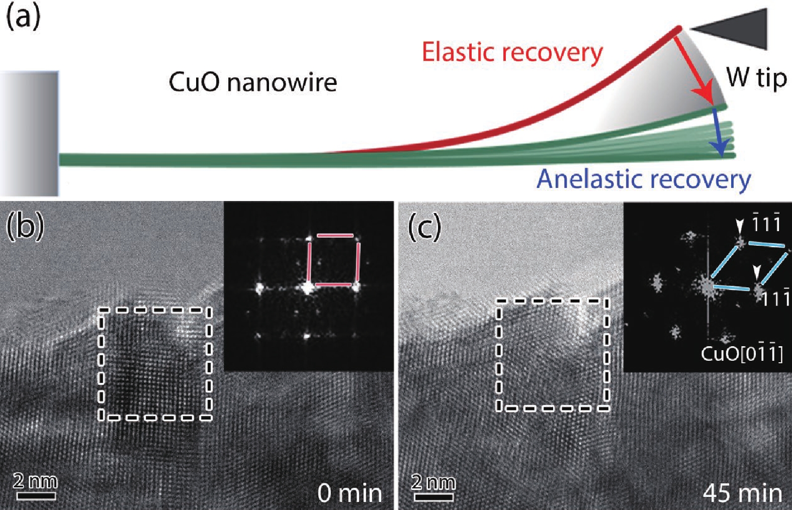
Figure 1.(Color online) Anelasticity in CuO induced by the point defects migration[
The phase boundaries between CuO0.67 and CuO represent the possible point defect diffusion pathways (Fig. 2(a)). Accordingly, three possible pathways (
![]()
Figure 2.(Color online) Oxygen vacancy diffusion pathways in CuO[
Apart from the defect behaviors, phase transition could be another deformation mechanism related with the plasticity in MOS. For instance, there are three kinds of structures in bulk ZnO—wurtzite (WZ), zinc blende (ZB), and rock salt (RS) structures[
![]()
Figure 3.(Color online) The phase transition of ZnO NW with
To clarify the underlying phase transition mechanisms, the surface and bulk energies of the NW with WZ, h-MgO, and BCT structures (Fig. 4(a)) under different tensile strains were calculated. A phase diagram related to the width and thickness of the NW, under 0% and 7% strain is presented in Fig. 4(b). The results elucidate that both the sample morphology and strain play important roles in mediating the phase stability of ZnO, which is consistent with the previous reports[
![]()
Figure 4.(Color online) The phase stability of WZ, h-MgO, and BCT structures in ZnO[
3. Influence of e-beam irradiation
Although the high-energy electrons inside TEM can provide ultra-high spatial (e.g. sub-Å) and energy resolution for imaging and elemental analysis[
Here, by taking CuO and ZnO as examples, we show our attempt to minimize the possible irradiation effects on the deformation behaviors. The irradiation effects on the structural changes in CuO and ZnO nanomaterials have been investigated[
![]()
Figure 5.(Color online) The effects of e-beam irradiation on the anelasticity in CuO NWs[
![]()
Figure 6.The phase transition of ZnO NW by applying 200 kV e-beam[
4. Conclusion and perspectives
With the continuous development of ultra-high resolution and NEMS systems, in-situ TEM plays a key role in the study of the structure-property relationship of MOSs. In this review, the mechanical deformation mechanisms of low-dimensional MOS have been studied and discussed at the atomic scale. These findings could provide first-hand experimental basis for rational and optimized design of MOS-based nanodevices from the smallest bottom. However, the basic material physics and chemistry of MOS has remained mysterious considering the complex defect structures. The interaction of different types of defects subjected to various kinds of external mechanical stress (e.g., tension, compression, and bending, etc.) remains largely unexplored. The effects of size, morphology, and mechanical loading directions on the mechanical behaviors have to be clarified. In addition, the atomistic view of the defect-induced electronic structure changes is far from well-known, which could be resolved by the newly developed segmented annular all field (SAAF) technique[
Acknowledgements
This work was supported by the National Natural Science Foundation of China (52071237, 12074290, 51871169, 51671148, 11674251, 51601132, 52101021, and 12104345), the Natural Science Foundation of Jiangsu Province (BK20191187), the Fundamental Research Funds for the Central Universities (2042019kf0190), the Science and Technology Program of Shenzhen (JCYJ20190808150407522) and the China Postdoctoral Science Foundation (2019M652685).
References
[1] J Z Sheng, K L Han, T H Hong et al. Review of recent progresses on flexible oxide semiconductor thin film transistors based on atomic layer deposition processes. J Semicond, 39, 011008(2018).
[2] J S Park, H Kim, I D Kim. Overview of electroceramic materials for oxide semiconductor thin film transistors. J Electroceram, 32, 117(2014).
[3] C L Dos Santos, P Piquini. Diameter dependence of mechanical, electronic, and structural properties of InAs and InP nanowires: a first-principles study. Phys Rev B, 81, 075408(2010).
[4] Y S Rim, H J Chen, B W Zhu et al. Interface engineering of metal oxide semiconductors for biosensing applications. Adv Mater Interfaces, 4, 1700020(2017).
[5] G Csiszar, R Lawitzki, C Everett et al. Elastic behavior of Nb2O5/Al2O3 core-shell nanowires in terms of short-range-order structures. ACS Appl Mater Interfaces, 13, 24238(2021).
[6] A Dey. Semiconductor metal oxide gas sensors: a review. Mat Sci Eng B, 229, 206(2018).
[7] S Li, M Zhang, H Wang. Simulation of gas sensing mechanism of porous metal oxide semiconductor sensor based on finite element analysis. Sci Rep, 11, 17158(2021).
[8] Y J Ke, J W Chen, G J Lin et al. Smart windows: electro-, thermo-, mechano-, photochromics, and beyond. Adv Energy Mater, 9, 1902066(2019).
[9] L Alus, O Brontvein, A Kossoy et al. Aligned growth of semiconductor nanowires on scratched amorphous substrates. Adv Funct Mater, 31, 2103950(2021).
[10] H D Chen, Z Zhang, B J Huang et al. Progress in complementary metal-oxide-semiconductor silicon photonics and optoelectronic integrated circuits. J Semicond, 36, 121001(2015).
[11] J Troughton, D Atkinson. Amorphous InGaZnO and metal oxide semiconductor devices: an overview and current status. J Mater Chem C, 7, 12388(2019).
[12] A Perrotta, J Pilz, A Milella et al. Opto-chemical control through thermal treatment of plasma enhanced atomic layer deposited ZnO: an in situ study. Appl Surf Sci, 483, 10(2019).
[13] A I Hofmann, E Cloutet, G Hadziioannou. Materials for transparent electrodes: from metal oxides to organic alternatives. Adv Electron Mater, 4, 1700412(2018).
[14] X Yu, T J Marks, A Facchetti. Metal oxides for optoelectronic applications. Nat Mater, 15, 383(2016).
[15] L H Wang, D L Kong, T J Xin et al. Deformation mechanisms of bent Si nanowires governed by the sign and magnitude of strain. Appl Phys Lett, 108, 151903(2016).
[16] R A Minamisawa, M J Suess, R Spolenak et al. Top-down fabricated silicon nanowires under tensile elastic strain up to 4.5%. Nat Commun, 3, 1096(2012).
[17] C Zhang, D G Kvashnin, L Bourgeois et al. Mechanical, electrical, and crystallographic property dynamics of bent and strained Ge/Si core-shell nanowires as revealed by in situ transmission electron microscopy. Nano Lett, 18, 7238(2018).
[18] X Han, L Kou, X Lang et al. Electronic and mechanical coupling in bent ZnO nanowires. Adv Mater, 21, 4937(2009).
[19] J Li, Z W Shan, E Ma. Elastic strain engineering for unprecedented materials properties. MRS Bull, 39, 108(2014).
[20] L Jia, D J Shu, M Wang. Tuning the area percentage of reactive surface of TiO2 by strain engineering. Phys Rev Lett, 109, 156104(2012).
[21] L Thulin, J Guerra. Calculations of strain-modified anatase TiO2 band structures. Phys Rev B, 77, 195112(2008).
[22] B Lim, X Y Cui, S P Ringer. Strain-mediated bandgap engineering of straight and bent semiconductor nanowires. Phys Chem Chem Phys, 23, 5407(2021).
[23] P T Bao, Y B Wang, X Y Cui et al. Atomic-scale observation of parallel development of super elasticity and reversible plasticity in GaAs nanowires. Appl Phys Lett, 104, 021904(2014).
[24] B Chen, Q Gao, Y B Wang et al. Anelastic behavior in GaAs semiconductor nanowires. Nano Lett, 13, 3169(2013).
[25] X D Han, Y F Zhang, K Zheng et al. Low-temperature in situ large strain plasticity of ceramic SiC nanowires and its atomic-scale mechanism. Nano Lett, 7, 452(2007).
[26] B Wei, K Zheng, Y Ji et al. Size-dependent bandgap modulation of ZnO nanowires by tensile strain. Nano Lett, 12, 4595(2012).
[27] H P Sheng, H Zheng, F Cao et al. Anelasticity of twinned CuO nanowires. Nano Res, 8, 3687(2015).
[28] B Varghese, Y Zhang, Y P Feng et al. Probing the size-structure-property correlation of individual nanowires. Phys Rev B, 79, 115419(2009).
[29] K H Liu, W L Wang, Z Xu et al. In situ probing mechanical properties of individual tungsten oxide nanowires directly grown on tungsten tips inside transmission electron microscope. Appl Phys Lett, 89, 221908(2006).
[30] R Agrawal, J T Paci, H D Espinosa. Large-scale density functional theory investigation of failure modes in ZnO nanowires. Nano Lett, 10, 3432(2010).
[31] L H Wang, Z Zhang, X D Han. In situ experimental mechanics of nanomaterials at the atomic scale. npg Asia Mater, 5, e40(2013).
[32] H Zheng, F Cao, L Zhao et al. Atomistic and dynamic structural characterizations in low-dimensional materials: recent applications of in situ transmission electron microscopy. Microscopy, 68, 423(2019).
[33] H Sheng, H Zheng, S Jia et al. Atomistic manipulation of reversible oxidation and reduction in Ag with an electron beam. Nanoscale, 11, 10756(2019).
[34] H H Liu, H Zheng, L Li et al. Surface-coating-mediated electrochemical performance in CuO nanowires during the sodiation-desodiation cycling. Adv Mater Interfaces, 5, 1701255(2018).
[35] S Jia, S Hu, H Zheng et al. Atomistic interface dynamics in Sn-catalyzed growth of wurtzite and zinc-blende ZnO nanowires. Nano Lett, 18, 4095(2018).
[36] H Zheng, J Wang, J Y Huang et al. Void-assisted plasticity in Ag nanowires with a single twin structure. Nanoscale, 6, 9574(2014).
[37] H Zheng, J Wang, J Y Huang et al. In situ visualization of birth and annihilation of grain boundaries in an Au nanocrystal. Phys Rev Lett, 109, 225501(2012).
[38] J Zhang, Y Li, X Li et al. Timely and atomic-resolved high-temperature mechanical investigation of ductile fracture and atomistic mechanisms of tungsten. Nat Commun, 12, 2218(2021).
[39] S Chen, H S Oh, B Gludovatz et al. Real-time observations of TRIP-induced ultrahigh strain hardening in a dual-phase CrMnFeCoNi high-entropy alloy. Nat Commun, 11, 826(2020).
[40] B Y Liu, F Liu, N Yang et al. Large plasticity in magnesium mediated by pyramidal dislocations. Science, 365, 73(2019).
[41] S Wang, Z Shan, H Huang. The mechanical properties of nanowires. Adv Sci, 4, 1600332(2017).
[42] J Y Huang, H Zheng, S X Mao et al. In situ nanomechanics of GaN nanowires. Nano Lett, 11, 1618(2011).
[43] L L Huang, F Y Zheng, Q M Deng et al. In situ scanning transmission electron microscopy observations of fracture at the atomic scale. Phys Rev Lett, 125, 246102(2020).
[44] R Agrawal, B Peng, H D Espinosa. Experimental-computational investigation of ZnO nanowires strength and fracture. Nano Lett, 9, 4177(2009).
[45] Q Wang, J Wang, J Li et al. Consecutive crystallographic reorientations and superplasticity in body-centered cubic niobium nanowires. Sci Adv, 4, eaas8850(2018).
[46] L H Wang, P Liu, P Guan et al. In situ atomic-scale observation of continuous and reversible lattice deformation beyond the elastic limit. Nat Commun, 4, 2413(2013).
[47] J C Stinville, M A Charpagne, F Bourdin et al. Measurement of elastic and rotation fields during irreversible deformation using Heaviside-digital image correlation. Mater Charact, 169, 110600(2020).
[48] R Agrawal, B Peng, E E Gdoutos et al. Elasticity size effects in ZnO nanowires – a combined experimental-computational approach. Nano Lett, 8, 3668(2008).
[49] G Wang, X Li. Size dependency of the elastic modulus of ZnO nanowires: Surface stress effect. Appl Phys Lett, 91, 242(2007).
[50] J Wang, A J Kulkarni, F J Ke et al. Novel mechanical behavior of ZnO nanorods. Comput Methods Appl Mech Eng, 197, 3182(2008).
[51] F Cao, L Li, H Zheng et al. Controllable elasticity storage and release in CuO-Pt core-shell nanowires. ChemNanoMat, 4, 1140(2018).
[52] K O Egbo, C P Liu, C E Ekuma et al. Vacancy defects induced changes in the electronic and optical properties of NiO studied by spectroscopic ellipsometry and first-principles calculations. J Appl Phys, 128, 135705(2020).
[53] J Zhang, J Shi, D C Qi et al. Recent progress on the electronic structure, defect, and doping properties of Ga2O3. APL Mater, 8, 020906(2020).
[54] Z Lu, B Huang, G Li et al. Shear induced deformation twinning evolution in thermoelectric InSb. npj Comput Mater, 7, 111(2021).
[55] S Wei, Q Wang, H Wei et al. Bending-induced deformation twinning in body-centered cubic tungsten nanowires. Mater Res Lett, 7, 210(2019).
[56] J Wang, Z Zeng, M Wen et al. Anti-twinning in nanoscale tungsten. Sci Adv, 6, eaay2792(2020).
[57] Y Chen, T Burgess, X An et al. Effect of a high density of stacking faults on the Young's modulus of GaAs nanowires. Nano Lett, 16, 1911(2016).
[58] F Mignerot, B Kedjar, H Bahsoun et al. Size-induced twinning in InSb semiconductor during room temperature deformation. Sci Rep, 11, 19441(2021).
[59] S Dai, J Zhao, M R He et al. Elastic properties of GaN nanowires: revealing the influence of planar defects on Young's modulus at nanoscale. Nano Lett, 15, 8(2015).
[60] F Cao, S F Jia, H Zheng et al. Thermal-induced formation of domain structures in CuO nanomaterials. Phys Rev Mater, 1, 053401(2017).
[61] L Wang, K Zheng, Z Zhang et al. Direct atomic-scale imaging about the mechanisms of ultralarge bent straining in Si nanowires. Nano Lett, 11, 2382(2011).
[62] G Dhanaraj, M Dudley, D Bliss et al. Growth and process induced dislocations in zinc oxide crystals. J Cryst Growth, 297, 74(2006).
[63] X Wang, K Chen, Y Zhang et al. Growth conditions control the elastic and electrical properties of ZnO nanowires. Nano Lett, 15, 7886(2015).
[64] K Choudhary, T Liang, A Chernatynskiy et al. Charge optimized many-body (COMB) potential for Al2O3 materials, interfaces, and nanostructures. J Phys: Condens Matter, 27, 305004(2015).
[65] W S Gorski. Theorie der elastischen nachwirkung in ungeordneten mischkristallen zweiter. Phys Z Sowj, 8, 457(1935).
[66] G Schaumann, J Völki, G Alefeld. The diffusion coefficients of hydrogen and deuterium in vanadium, niobium, and tantalum by gorsky-effect measurements. Phys Status Solidi B, 42, 401(1970).
[67] G Schaumann, J Völkl, G Alefeld. Relaxation process due to long-range diffusion of hydrogen and deuterium in niobium. Phys Rev Lett, 21, 891(1968).
[68] G M Cheng, C Y Miao, Q Q Qin et al. Large anelasticity and associated energy dissipation in single-crystalline nanowires. Nat Nanotech, 10, 687(2015).
[69] L Li, G Chen, H Zheng et al. Room-temperature oxygen vacancy migration induced reversible phase transformation during the anelastic deformation in CuO. Nat Commun, 12, 3863(2021).
[70] X Sun, W Zhu, D Wu et al. Surface-reaction induced structural oscillations in the subsurface. Nat Commun, 11, 305(2020).
[71] Z L Wang. ZnO nanowire and nanobelt platform for nanotechnology. Mater Sci Eng R, 64, 33(2009).
[72] C L Freeman, F Claeyssens, N L Allan et al. Graphitic nanofilms as precursors to wurtzite films: theory. Phys Rev Lett, 96, 066102(2006).
[73] B J Morgan. First-principles study of epitaxial strain as a method of B4→BCT stabilization in ZnO, ZnS, and CdS. Phys Rev B, 82, 153408(2010).
[74] M Jeannin, A Artioli, P Rueda-Fonseca et al. Light-hole exciton in a nanowire quantum dot. Phys Rev B, 95, 035305(2017).
[75] L Sponza, J Goniakowski, C Noguera. Confinement effects in ultrathin ZnO polymorph films: electronic and optical properties. Phys Rev B, 93, 195435(2016).
[76] S Yamamoto, T Mishina. Observation of dark exciton luminescence from ZnO nanocrystals in the quantum confinement regime. Phys Rev B, 83, 165435(2011).
[77] X Zhao, C M Wei, L Yang et al. Quantum confinement and electronic properties of silicon nanowires. Phys Rev Lett, 92, 236805(2004).
[78] B H Liu, M E Mcbriarty, M J Bedzyk et al. Structural transformations of zinc oxide layers on Pt(111). J Phys Chem C, 118, 28725(2014).
[79] X Y Deng, K Yao, K J Sun et al. Growth of single- and bilayer ZnO on Au(111) and interaction with copper. J Phys Chem C, 246, 11211(2013).
[80] G Weirum, G Barcaro, A Fortunelli et al. Growth and surface structure of zinc oxide layers on a Pd(111) surface. J Phys Chem C, 114, 15432(2010).
[81] P L Zhao, X X Guan, H Zheng et al. Surface- and strain-mediated reversible phase transformation in quantum-confined ZnO nanowires. Phys Rev Lett, 123, 216101(2019).
[82] A J Kulkarni, M Zhou, K Sarasamak et al. Novel phase transformation in ZnO nanowires under tensile loading. Phys Rev Lett, 97, 105502(2006).
[83] J Wang, A J Kulkarni, K Sarasamak et al. Molecular dynamics and density functional studies of a body-centered-tetragonal polymorph of ZnO. Phys Rev B, 76, 172103(2007).
[84] N Jiang. Electron beam damage in oxides: a review. Rep Prog Phys, 79, 016501(2016).
[85] R F Egerton, P Li, M Malac. Radiation damage in the TEM and SEM. Micron, 35, 399(2004).
[86] T Susi, J C Meyer, J Kotakoski. Quantifying transmission electron microscopy irradiation effects using two-dimensional materials. Nat Rev Phys, 1, 397(2019).
[87] S B Lee. Rocksalt ZnO nanocrystal formation by beam irradiation of wurtzite ZnO in a transmission electron microscope. Physica E, 84, 310(2016).
[88] L L Zhao, L Li, H P Sheng et al. Atomistic insight into ordered defect superstructures at novel grain boundaries in CuO nanosheets: From structures to electronic properties. Nano Res, 12, 1099(2019).
[89] S F Jia, L Li, L L Zhao et al. Surface-dependent formation of Zn clusters in ZnO single crystals by electron irradiation. Phys Rev Mater, 2, 060402(2018).
[90] D C Look, J W Hemsky, J R Sizelove. Residual native shallow donor in ZnO. Phys Rev Lett, 82, 2552(1999).
[91] C Coskun, D C Look, G C Farlow et al. Radiation hardness of ZnO at low temperatures. Semicond Sci Technol, 19, 752(2004).
[92] S O Kucheyev, C Jagadish, J S Williams et al. Implant isolation of ZnO. J Appl Phys, 93, 2972(2003).
[93] K Ooe, T Seki, Y Ikuhara et al. High contrast STEM imaging for light elements by an annular segmented detector. Ultramicroscopy, 202, 148(2019).
[94] R Ishikawa, S D Findlay, T Seki et al. Direct electric field imaging of graphene defects. Nat Commun, 9, 3878(2018).
[95] N Shibata, S D Findlay, Y Kohno et al. Differential phase-contrast microscopy at atomic resolution. Nat Phys, 8, 611(2012).
[96] T Lee, F A Mas'ud, M J Kim et al. Spatially resolved Raman spectroscopy of defects, strains, and strain fluctuations in domain structures of monolayer graphene. Sci Rep, 7, 16681(2017).
[97] M Huang, H Yan, T F Heinz et al. Probing strain-induced electronic structure change in graphene by Raman spectroscopy. Nano Lett, 10, 4074(2010).
[98] C A Dennett, Z Hua, A Khanolkar et al. The influence of lattice defects, recombination, and clustering on thermal transport in single crystal thorium dioxide. APL Mater, 8, 111103(2020).


Set citation alerts for the article
Please enter your email address

© Copyright 2018-2021 | Chinese Laser Press. All Rights Reserved 沪ICP备15018463号-20