
Ye Yuan, Shengqiang Zhou, Xinqiang Wang. Modulating properties by light ion irradiation: From novel functional materials to semiconductor power devices[J]. Journal of Semiconductors, 2022, 43(6): 063101
- Journal of Semiconductors
- Vol. 43, Issue 6, 063101 (2022)
Abstract
1. Introduction
Ion beams present a variety of useful functions in the field of semiconductors, acting as the state-of-the-art tools for both basic research and industry. In particular, it is worth noting that ion implantation has been integrated as one of the most crucial processes in modern IC industry[
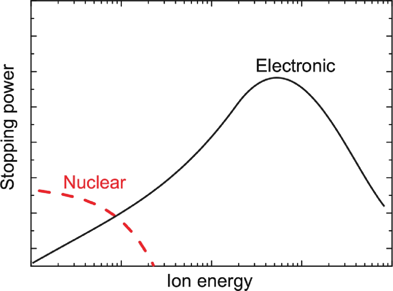
In addition to the above-mentioned well-known doping contributions introduced by implanted ions themselves, point defects are spontaneously produced in the semiconductor matrix due to the collisions between incident ions and the matrix atoms. The interaction between implanted ions and target atoms could be briefly described as follows: by undergoing collisions with the electron system and the nuclei of the target matrix, the impinged ions gradually lose the kinetic energy. At the very beginning, the kinetic energy loss is mainly caused by the electronic stopping (excitation and inelastic atom ionization), which dominates in the high energy regime. In such a regime, the implanted ions prefer a straight moving path, and the main stopping mechanism of interaction mainly comes from the inelastic interactions between bound electrons in the matrix atoms and the implanted ions. Therefore, the inelastic interaction is highlighted to be responsible for the energy lost, accordingly, this part of transferred energy is partially dissipated by phonons; however, the displacement of lattice atoms seldomly happens. Afterwards, upon penetrating into deeper depth, the implanted ions start to confront nuclear stopping due to their low kinetic energy, in which the displacement of atoms starts to dominate and even leads to a cascade of recoiled atoms. This process is named nuclear stopping, which mainly refers to the elastic instead of inelastic collisions between the projectile ions and matrix atoms in the target. It is worth noting that the nuclear stopping means that this type of stopping involves the collision of the ion with the nuclei in the target. At this moment, the point defects start to accumulate. A schematic of relative loss of kinetic energy is shown in Fig. 1 to make a comparison between electronic and nuclear stopping processes with their dependence on ion kinetic energy[
![]()
Figure 1.(Color online) Schematic of the cross-section for electronic and nuclear stopping processes as a function of ion energy[
The above-mentioned point defects can provide additional functionalities in semiconductor materials. In particular, light ions (e.g., proton, helium as well as some other ions whose atomic numbers are relatively small) are beneficial for a better access of thick films/devices, as well as for a gentle control of the number of defects without inducing amorphization. Therefore, light ion irradiation is becoming more attractive in both condense matter physics and semiconductor techniques. From the basic research viewpoint, the generated various vacancies or interstitials act as potential disorder, which in principle affects the electrical-transport properties (e.g., carrier mobility), and therefore highlights the contribution of Anderson localization[
In this short review, we will only focus on the application of light ion irradiation in tailoring the electronic properties of emerging functional materials[
2. Manipulating defects in conventional and novel functional materials
2.1. Tuning the Fermi level in dilute ferromagnetic semiconductors
Dilute ferromagnetic semiconductors (DFSs) have been viewed as the one of the most fancy topics in the past several decades. Due to the nature of hole-mediated ferromagnetism in DFSs, any methods used in tuning carrier concentration[
Since the discovery of DFSs, the mechanism of hole-mediated ferromagnetism has always been placed at the center of the argument, where the competition between p-d Zener model and the impurity model never stops. In the p-d Zener model the randomly distributed Mn moments are bridged by the itinerant valence band holes[
![]()
Figure 2.(Color online) Magnetic properties after introducing hole compensation by ion irradiation. The ion fluence was increased in linear steps. (a), (c), and (d) show the temperature dependent magnetization for different samples, while (b) shows the magnetic hysteresis for sample Mn6ann (GaMnAs) for various ion fluences. The temperature-dependent magnetization is measured at a small field of 20 Oe after cooling in field. One observes an increase in the coercive field
Besides the most widely studied GaAs based DFSs, the proton irradiation can also stabilize the Fermi level in relatively different positions in the bandgap in various III–V matrixes[
![]()
Figure 3.(Color online) (a) Curie temperature (
In addition to the dilute magnetic semiconductors whose properties are strongly coupled by carriers, plenty of novel proposed functional materials also require such a method of carrier-modulation. In particular, the recently exotic topological properties in various topological materials are also reflected through electrical carriers; therefore, the ion irradiation would definitely be an ideal tool for investigation.
2.2. Generating potential disorder in topological materials
In addition to modifying the Fermi level by introducing carrier compensation, in some cases, the structural or potential disorders caused by irradiation induced defects can significantly influence electrical-transport properties, even though the carrier concentration remains constant[
By borrowing the concept of Fermi level tuning in DFSs, the validity of manipulating carrier type or concentration through irradiation in a canonical topological insulator Bi2Te3 has been tested[
SF is the cross section of the Fermi surface perpendicular to the direction of the field B, mc is the cyclotron mass,
where
![]()
Figure 4.(Color online) (a) Oscillating part of the resistivity
where the
Following the above discussion, the irradiation induced defects not only compensate carriers, but also produce electrical disorder which violates the highly ordered Bloch potential. It is well-known that in a material with low mobility, the contribution of compensation is mainly in charge; however, in a high mobility system, the disorder effect starts to dominate. As described in Fig. 4(d), the mean free path reduces in half and saturates when the fluence is 43 mC/cm2, which is indicative that the contribution of electrical disorder is comparable with that from the Fermi energy shift. Subsequently, such a disorder is treated as a meaningful tool to investigate the disorder contribution in other topological materials, such as NbxBi2Se3[
![]()
Figure 5.(Color online) Low-temperature variation of the London penetration depth Δλ(
According to this description, the ion irradiation is useful in modifying physical properties, which is related in carrier density in various functional materials. This carrier compensation contribution is strongly expected in application, due to its flexibility and manipulability. Therefore, in the next section, the employment of compensation caused by irradiation will be reviewed in improving the performance of electrical and electronic devices.
3. Manipulating the dynamic properties in semiconductor power devices
The explosion of electric power employment, particularly the preliminary success of electric-vehicles, is raising the unprecedented demand for p–n diode power devices. The switching speed (in particular switch-off) of these devices is becoming crucial for evaluating the comprehensive performance, particularly in high-frequency applications. The switch-off process can be described as follows: when the opposite voltage is applied in the p–n diode, current flows through the diode in the opposite direction and spends some time to arrive at the stable state. During this process, the free minority carriers are first neutralized in both p and n regions and subsequently the carriers start to move and construct the depletion region. Accordingly, the whole period is called reverse recovery time and decides the switch-off speed. The expectation of improving dynamic performance starts the employment of light ion irradiation technique to tune the lifetime of the carriers. Although some conventional approaches such as diffusion life-killers have been maturely used in Si-based power devices, some shortages (e.g., short diffusion length or low sensitivity) still prohibit their utility in SiC-based devices[
3.1. SiC semiconductor and SiC power device
Distinctive sets of defects in SiC are produced by irradiation, and the deep level transient spectrum (DLTS) is often employed to identify deep level defects. As shown in Fig. 6, Hazdra et al.’s results are present in fast neutrons, electrons, protons as well as carbon ions irradiated n-type 4H-SiC[
![]()
Figure 6.(Color online) DLTS spectra of 4H-SiC n-type epilayer irradiated with (a) fast neutrons, (b) 4.5 MeV electrons, (c) 670 keV protons, and (d) 9.6 MeV carbon ions. First temperature scan, rate window 4.1 s−1 (neutron, proton and carbon irradiation) and 56 s−1 (electrons)[
To modulate the carrier lifetime, several approaches have been employed to demonstrate or excavate the function of Z1/2 before the light ion irradiation technique is imported: the annihilation of Z1/2 defects extends the carrier lifetime. For instance, several studies have shown that the carrier lifetime in carbon-implanted SiC is increased by high temperature annealing[
![]()
Figure 7.(Color online) DLTS spectra of n-base of the 4H-SiC PiN diode measured before (black thin) and after (short-dashed) irradiation with 800 keV protons to a fluence of 5 × 109 cm–2 and after annealing at 370 °C (red thick)[
Z1/2 locates at about 0.44 eV below the bottom of the conduction band, acting as the main local lifetime killer in terms of its large capture cross section for both electrons and holes. When Z1/2 centers are placed in the n-region of p–n diode junction, the electrons (majority carriers) are strongly compensated in the defect-profiled space, therefore speeding up the device turn-off process. On the basis of the study from Hazdra et al.[
![]()
Figure 8.(Color online) Reverse recovery of the 2 A/10 keV SiC PiN diode measured before (solid line) and after irradiation (dashed-dotted line) with 800 keV protons to a fluence of 1 × 1011 cm–1 and after subsequent 1 h annealing at 370 °C (dash line) [
![]()
Figure 9.(Color online) Measured OCVD response of 4H-SiC PiN diodes irradiated with different fluences of 800 keV protons. The value of high-level lifetime
In addition to the most wanted Z1/2-type defect, the SiC based p–n device is unavoidably affected by other various type defects, of which the most crucial one is EH6/7, whose thermo-stabilization is at the same level as Z1/2. EH6/7 lies 1.64 eV below the bottom of conduction band (even in the center of the bandgap), which is much deeper than Z1/2. As a consequence, they work as charge producer in the space charge region, leading to the diode leakage (off state losses) in irradiated devices. Another negative effect brought by deep level traps is the increase of the forward voltage drop due to the compensation induced electron reduction, which has been observed in a set of various SiC based devices, e.g. PiN diode[
3.2. Si semiconductor and Si power device
Despite the fact that many alternative candidates (e.g., SiC or GaN) have been attracting attention, silicon still occupies the main part of power device market due to its mature industrial process. Thus, it is meaningful to review the manipulation of silicon as well as the corresponding device modified by light ion irradiation. Indeed, the irradiation contribution to silicon devices initiated the followed-up activities in SiC diodes, including IGBTs[
![]()
Figure 10.(Color online) Majority carrier DLTS spectra of P+PN–N+ diode measured after (a) He+ irradiation and (b) H+ and isochronal 40 min annealing at 220 and 350 °C, rate window 260 s–1 [
The exploration of tuning life-time in silicon p–n type device has been performed in the past decades. As shown in Fig. 11, when the irradiation project range is placed in different depth (e.g., the anode side of the junction inside (outside) of the space charge region) and the N base side of the junction, their distinct contribution works on the lifetime of the p–n device[
![]()
Figure 11.(a) Current reverse recovery characteristics of diodes irradiated by 500 keV (3 × 1014 cm–2) and 4 MeV (2 × 1013 cm–2) electrons (solid thin) and H+/He2+ ions (fluence 5 × 10¹² / 5 × 1011 cm–2, thick solid/dashed); (b) current (solid) and voltage (dashed) reverse recovery characteristics of the unirradiated diode and diodes irradiated by 4 MeV (2 × 1013 cm–2) electrons and H+ ions (fluence 5 × 1012 cm–2)[
The trade-off that happens in SiC devices is also inevitable in Si: the fast switch-off process is always accompanied with the sacrifice of forward voltage and current leakage. Of all generated defects, E5 is always treated as the charging role who is responsible for the leakage, which is attributed to its location in the middle of the bandgap[
![]()
Figure 12.The reverse
![]()
Figure 13.Trade-off between the ON-state voltage drop at 100 A and the turn-OFF losses measured at (a)
Finally, it is worth noting that herein we only reviewed the application of ion beams in two types of functional materials and semiconductor devices. The ion beam only provides an avenue for modifying Fermi level in materials, and it could be expanded in any other materials. It could be utilized as long as various new functional materials are developed; for example the ion beam modification is recently employed in very hot 2D materials[
4. Summary
In summary, the application of light ion (proton or alpha particle) or electron irradiation in modulating the properties of both novel functional materials and PIN power devices has been systematic reviewed. By properly employing the irradiation-induced defects, which generally act as carrier traps, it is possible to precisely tune the carrier concentration. This compensation can be used to study/tune some properties that are determined by the carrier concentration (e.g., the Curie temperature, magnetization as well as uniaxial magnetic anisotropy in dilute ferromagnetic semiconductors or electrical-transport properties in topological materials). The compensation reduces the carrier’s life-time, which directly contributes to improving the dynamic performance of Si or SiC based PiN power devices, although several static performance parameters, including the forward voltage and current leakage, are somehow sacrificed. Nevertheless, this trade-off has been well played to fulfill different application requirements. Considering the explosion of novel functional materials and the energy revolution, it is believed that the light ion irradiation technique will find favor in both fundamental research and industrial applications.
Acknowledgements
This work was supported by Key-Area Research and Development Program of Guangdong Province (No. 2019B010132001). This work was also partially funded by Guangdong Basic and Applied Basic Research Foundation (2020A1515110891).
References
[1] J Mayer, O Marsh. Ion implantation in semiconductors. Appl Solid State Sci, 1, 239(1969).
[2]
[3] Y Yuan, C Xu, R Hübner et al. Interplay between localization and magnetism in (Ga, Mn)As and (In, Mn)As. Phys Rev Mater, 1, 054401(2017).
[4] Y Yuan, Y Wang, M Khalid et al. Ferromagnetic GaMnP prepared by ion implantation and pulsed laser annealing. IEEE Trans Mag, 50, 2401304(2014).
[5] Y Yuan, M Wang, C Xu et al. Electronic phase separation in insulating (Ga, Mn)As with low compensation: Super-paramagnetism and hopping conduction. J Phys Condens Matter, 30, 095801(2018).
[6] Y Yuan, R Hübner, F Liu et al. Ferromagnetic Mn-implanted GaP: Microstructures vs magnetic properties. ACS Appl Mater & Interfaces, 8, 3912(2016).
[7] Y Yuan, g Y Wang, o K Gao et al. High Curie temperature and perpendicular magnetic anisotropy in homoepitaxial InMnAs films. J Phys D, 48, 235002(2015).
[8] S Prucnal, V Heera, R Hübner et al. Superconductivity in single-crystalline aluminum- and gallium-hyperdoped germanium. Phys Rev Mater, 3, 054802(2019).
[9] M Wang, Y Berencén, E García-Hemme et al. Extended infrared photoresponse in Te-hyperdoped Si at room temperature. Phys Rev Appl, 10, 024054(2018).
[10] F Liu, S Prucnal, Y Berencén et al. Realizing the insulator-to-metal transition in Se-hyperdoped Si via non-equilibrium material processing. J Phys D, 50, 415102(2017).
[11] J F Ziegler, r M D Ziegler, k J B Biersack. SRIM-The stopping and range of ions in matter (2010). Nucl Instrum Methods Phys Res Sect B, 268, 1818(2010).
[12] S Zhou, X L Chen. Defect-induced magnetism in SiC. J Phys D, 52, 393001(2019).
[13] P A Lee, T V Ramakrishnan. Disordered electronic systems. Rev Mod Phys, 57, 287(1985).
[14] S T Pantelides. The electronic structure of impurities and other point defects in semiconductors. Rev Mod Phys, 50, 797(1978).
[15] J Park, J H Choi, K Kong et al. Electrically driven mid-submicrometre pixelation of InGaN micro-light-emitting diode displays for augmented-reality glasses. Nat Photonics, 15, 449(2021).
[16] S Zhou, L Li, Y Yuan et al. Precise tuning of the Curie temperature of (Ga, Mn)As-based magnetic semiconductors by hole compensation: Support for valence-band ferromagnetism. Phy Rev B, 94, 075205(2016).
[17] C Xu, M Wang, Y Yuan et al. Hole compensation effect in III-Mn-V dilute ferromagnetic semiconductors. J Phys D, 52, 355301(2019).
[18] C W Rischau, B Leridon, B Fauqué et al. Doping of Bi2Te3 using electron irradiation. Phys Rev B, 88, 205207(2013).
[19] Y Liu, Z Li, L Guo et al. Towards diluted magnetism in TaAs. Phys Rev Mater, 1, 044203(2017).
[20] P Hazdra, S Popelka, A Schöner. Optimization of SiC power p-i-n diode parameters by proton irradiation. IEEE Trans Electron Devices, 65, 4483(2018).
[21] R K Sharma, P Hazdra, S Popelka. The effect of light ion irradiation on 4H-SiC MPS power diode characteristics: Experiment and simulation. IEEE Trans Nucl Sci, 62, 534(2015).
[22] B Aspar, M Bruel, H Moriceau et al. Basic mechanisms involved in the Smart-Cut® process. Microelectron J, 36, 233(1997).
[23] M Bruel, B Aspar, A J Auberton-Hervé. Smart-Cut: A new silicon on insulator material technology based on hydrogen implantation and wafer bonding. J Jpn Appl Phys, 36, 1636(1997).
[24] T Dietl, H Ohno, F Matsukura et al. Zener model description of ferromagnetism in zinc-blende magnetic semiconductors. Science, 287, 1019(2000).
[25] Yuan Y, Amarouche T, Xu C et al. Switching the uniaxial magnetic anisotropy by ion irradiation induced compensation. J Phys D, 51, 145001(2018).
[26] M Dobrowolska, K Tivakornsasithorn, X Liu et al. Controlling the Curie temperature in (Ga, Mn)As through location of the Fermi level within the impurity band. Nat Mater, 11, 444(2012).
[27] S T B Goennenwein, T A Wassner, H Huebl et al. Hydrogen control of ferromagnetism in a dilute magnetic semiconductor. Phys Rev Lett, 92, 227202(2004).
[28] E H C P Sinnecker, G M Penello, T G Rappoport et al. Ion-beam modification of the magnetic properties of Ga1−
[29] R Kudrawiec. Conduction and valence band positions versus the Fermi-level stabilization energy in quaternary dilute nitrides. Phys Status Solidi C, 8, 1650(2011).
[30] C Wang, C H Chang, A Huang et al. Tunable disorder and localization in the rare-earth nickelates. Phys Rev Mater, 3, 053801(2019).
[31] F Evers, A D Mirlin. Anderson transitions. Rev Mod Phys, 80, 1355(2008).
[32] M P Smylie, H Claus, W K Kwok et al. Superconductivity, pairing symmetry, and disorder in the doped topological insulator Sn1−
[33] V Harimohan, A Bharathi, R Rajaraman et al. Magneto-resistance in pristine and irradiated TaAs2. AIP Adv, 9, 045020(2019).
[34]
[35] A Hashibon, C Elsässer. First-principles density functional theory study of native point defects in Bi2Te3. Phys Rev B, 84, 144117(2011).
[36] P Pecheur, G Toussaint. Tight-binding studies of crystal stability and defects in Bi2Te3. J Phys Chem Solids, 55, 327(1994).
[37] P Chaudhari, M B Bever. Effects of irradiation with protons on the electrical properties of Bi2Te3. J Appl Phys, 37, 4181(1966).
[38] P Chaudhari, M B Bever. Defects in the compound Bi2Te3 caused by irradiation with protons. J Appl Phys, 38, 2417(1967).
[39] M P Smylie, K Willa, H Claus et al. Robust odd-parity superconductivity in the doped topological insulator Nb
[40]
[41] J Vobecký, P Hazdra, V Záhlava et al. ON-state characteristics of proton irradiated 4H–SiC Schottky diode: The calibration of model parameters for device simulation. Solid-State Electron, 94, 32(2014).
[42] J Vobecký, P Hazdra, S Sharma et al. Impact of electron irradiation on the On-state characteristics of a 4H-SiC JBS diode. IEEE Trans Electron Devices, 62, 1964(2015).
[43] T Hiyoshi, T Kimoto. Reduction of deep levels and improvement of carrier lifetime in n-type 4H-SiC by thermal oxidation. Appl Phys Express, 2, 041101(2009).
[44] P Hazdra, S Popelka, V Záhlava et al. Radiation damage in 4H-SiC and its effect on power device characteristics. Solid State Phenomena, 242, 421(2015).
[45] J S Williams. Ion implantation of semiconductors. Mater Sci Eng A, 253, 8(1998).
[46] A Hallén, S Janson M, A YuKuznetsov et al. Ion implantation of silicon carbide. Nucl Instrum Methods Phys Res Sect B, 186, 186(2002).
[47] J C Zolper. Ion implantation in group III-nitride semiconductors: a tool for doping and defect studies. J Crys Growth, 178, 157(1997).
[48] S J Pearton. Ion implantation in III–V semiconductor technology. Int J Mod Phys B, 7, 4687(1993).
[49] G Alfieri, E V Monakhov, B G Svensson et al. Annealing behavior between room temperature and 2000 °C of deep level defects in electron-irradiated n-type 4H silicon carbide. J Appl Phys, 98, 043518(2005).
[50] B Zippelius, J Suda, T Kimoto. High temperature annealing of n-type 4H-SiC: Impact on intrinsic defects and carrier lifetime. J Appl Phys, 111, 033515(2012).
[51] T Dalibor, G Pensl, H Matsunami et al. Deep defect centers in silicon carbide monitored with deep level transient spectroscopy. Phys Status Solidi A, 162, 199(1997).
[52] P B Klein, B V Shanabrook, S W Huh et al. Lifetime-limiting defects in n- 4H-SiC epilayers. Appl Phys Lett, 88, 052110(2006).
[53] I Pintilie, L Pintilie, K Irmscher et al. Formation of the Z1,2 deep-level defects in 4H-SiC epitaxial layers: Evidence for nitrogen participation. Appl Phys Lett, 81, 4841(2002).
[54] T A G Eberlein, R Jones, P R Briddon. Z1/Z2 defects in 4H-SiC. Phys Rev Lett, 90, 225502(2003).
[55] L Storasta, A Henry, J P Bergman et al. Investigations of possible nitrogen participation in the Z1/Z2 defect in 4H-SiC. Mater Sci Forum, 457–460, 469(2004).
[56] L Storasta, H Tsuchida. Reduction of traps and improvement of carrier lifetime in epilayers by ion implantation. Appl Phys Lett, 90, 062116(2007).
[57] L Storasta, H Tsuchida, T Miyazawa. Enhanced annealing of the Z1/2 defect in 4H–SiC epilayers. J Appl Phys, 103, 013705(2008).
[58] S Ichikawa, K Kawahara, J Suda et al. Carrier recombination in n-type 4H-SiC epilayers with long carrier lifetimes. Appl Phys Express, 5, 101301(2012).
[59] P Hazdra, S Popelka, A Schöner. Local lifetime control in 4H-SiC by proton irradiation. Mater Sci Forum, 924, 436(2018).
[60] N Achtziger, G Pasold, R Sielemann et al. Tungsten in silicon carbide: Band-gap states and their polytype dependence. Phys Rev B, 62, 12888(2000).
[61] C Hemmingsson, N T Son, O Kordina et al. Deep level defects in electron-irradiated 4H SiC epitaxial layers. J Appl Phys, 81, 6155(1997).
[62] L Storasta, J P Bergman, E Janzén et al. Deep levels created by low energy electron irradiation in 4H-SiC. J Appl Phys, 96, 4909(2004).
[63] P Hazdra, S Popelka. Lifetime control in SiC PiN diodes using radiation defects. Mater Sci Forum, 897, 463(2017).
[64] N T Son, X T Trinh, L S Løvlie et al. Negative-U system of carbon vacancy in 4H-SiC. Phys Rev Lett, 109, 187603(2012).
[65] J Vobecký, P Hazdra, V Záhlava. Open circuit voltage decay lifetime of ion irradiated devices. Microelectron J, 30, 513(1999).
[66] P Guerriero, A Sanseverino, S Daliento. Lifetime profile reconstruction in helium implanted silicon for planar IGBTs. 29th International Conference on Microelectronics Proceedings - MIEL 2014, Belgrade, 325(2014).
[67] P Hazdra, K Brand, J Rubeš et al. Local lifetime control by light ion irradiation: impact on blocking capability of power P–i–N diode. Microelectron J, 32, 449(2001).
[68] E Napoli, A G M Strollo, P Spirito. Numerical analysis of local lifetime control for high-speed low-loss P-i-N diode design. IEEE Trans Power Electron, 14, 615(1999).
[69] P Hazdra, V Komarnitskyy. Lifetime control in silicon power P-i-N diode by ion irradiation: Suppression of undesired leakage. Microelectron J, 37, 197(2006).
[70] I Kohno. Production of fast-switching power thyristors by proton irradiation. Nucl Instrum Methods Phys Res Sect B, 37/38, 739(1989).
[71] D C Sawko, J Bartko. Production of fast switching power thyristors by proton irradiation. IEEE Trans Nucl Sci, 30, 1756(1983).
[72] P Hazdra, K Brand, J Vobecky. Effect of defects produced by MeV H and He ion implantation on characteristic of power silicon P-i-N diodes. 2000 International Conference on Ion Implantation Technology, 135(2000).
[73] P Hazdra, J Vobecky, H Dorschner et al. Axial lifetime control in silicon power diodes by irradiation with protons, alphas, low- and high-energy electrons. Microelectron J, 35, 249(2004).
[74] P Hazdra, J Rubeš, J Vobecký. Divacancy profiles in MeV helium irradiated silicon from reverse I–V measurement. Nucl Instrum Methods Phys Res Sect B, 159, 207(1999).
[75] J Vobecky, P Hazdra, V Zahlava. Helium irradiated high-power P-i-N diode with low On-state voltage drop. Solid-State Electron, 47, 45(2003).
[76] J Vobecky, P Hazdra. The application of platinum-silicide anode layer to decrease the static and turn-off losses in high-power P-i-N diode. Thin Solid Films, 433, 305(2003).
[77] J Vobecky, P Hazdra. Advanced local lifetime control for higher reliability of power devices. Microelectron Reliab, 42, 1883(2003).
[78] A Prabhakar, T C McGill, M A Nicolet. Platinum diffusion into silicon from PtSi. Appl Phys Lett, 43, 1118(1983).
[79] D C Schmidt, G Svensson, S Godey et al. The influence of diffusion temperature and ion dose on proximity gettering of platinum in silicon implanted with alpha particles at low doses. Appl Phys Lett, 74, 3329(1999).
[80] D Seol, S Kim, W S Jang et al. Selective patterning of out-of-plane piezoelectricity in MoTe2 via focused ion beam. Nano Energy, 79, 105451(2021).
[81] E Mitterreiter, B Schuler, K A Cochrane et al. Atomistic positioning of defects in helium ion treated single-layer MoS2. Nano Lett, 20, 4437(2020).
[82] C Babin, R Stöhr, N Morioka et al. Fabrication and nanophotonic waveguide integration of silicon carbide colour centres with preserved spin-optical coherence. Nat Mater, 21, 67(2022).
[83] C Kasper, D Klenkert, Z Shang et al. Influence of irradiation on defect spin coherence in silicon carbide. Phys Rev Appl, 13, 044054(2020).
[84] M E Bathen, L Vines. Manipulating single-photon emission from point defects in diamond and silicon carbide. Adv Quantum Technol, 4, 2100003(2021).
[85] W Xiong, X Zhou, G Xu et al. Double-barrier-Ga2O3 Schottky barrier diode with low turn-on voltage and leakage current. IEEE Electron Device Lett, 42, 430(2021).
[86] Q He, W Hao, X Zhou et al. Over 1 GW/cm2 vertical Ga2O3 Schottky barrier diodes without edge termination. IEEE Electron Device Lett, 43, 264(2022).
[87] W Hao, Q He, K Zhou et al. Low defect density and small curve hysteresis in NiO/β-Ga2O3 pn diode with a high PFOM of 0.65 GW/cm2. Appl Phys Lett, 118, 043501(2021).
[88] X Hou, X Zhao, Y Zhang et al. High-performance harsh-environment-resistant GaO


Set citation alerts for the article
Please enter your email address

© Copyright 2018-2021 | Chinese Laser Press. All Rights Reserved 沪ICP备15018463号-20