
Xiaomei Wu, Xiaoxing Ke, Manling Sui. Recent progress on advanced transmission electron microscopy characterization for halide perovskite semiconductors[J]. Journal of Semiconductors, 2022, 43(4): 041106
- Journal of Semiconductors
- Vol. 43, Issue 4, 041106 (2022)
Abstract
1. Introduction
The fast rising of halide perovskites has drawn significant attention in the field of energy materials in the past decade. Owning to their unique structure, high degree of tunability, and excellent photoelectric properties, halide perovskites have been widely used in photovoltaic and optoelectronic devices, including solar cells, LED, and photodetectors[
The unusual optoelectronic properties and performance of halide perovskites are closely related to their unique crystal structure and microstructure. The name of the perovskite is originated from the calcium titanate (CaTiO3) compound in the perovskite mineral, and is referred to as ABX3 compound (where A and B are cations and X is an anion). In perovskite structure, [BX6] octahedra are corner-sharing to be ordered in a cubically, where the cations at A-site are located in the center of cubic cage[
Transmission electron microscopy (TEM) is one of the most straightforward characterization techniques to investigate the microstructure from nanometer to the atomic scale[
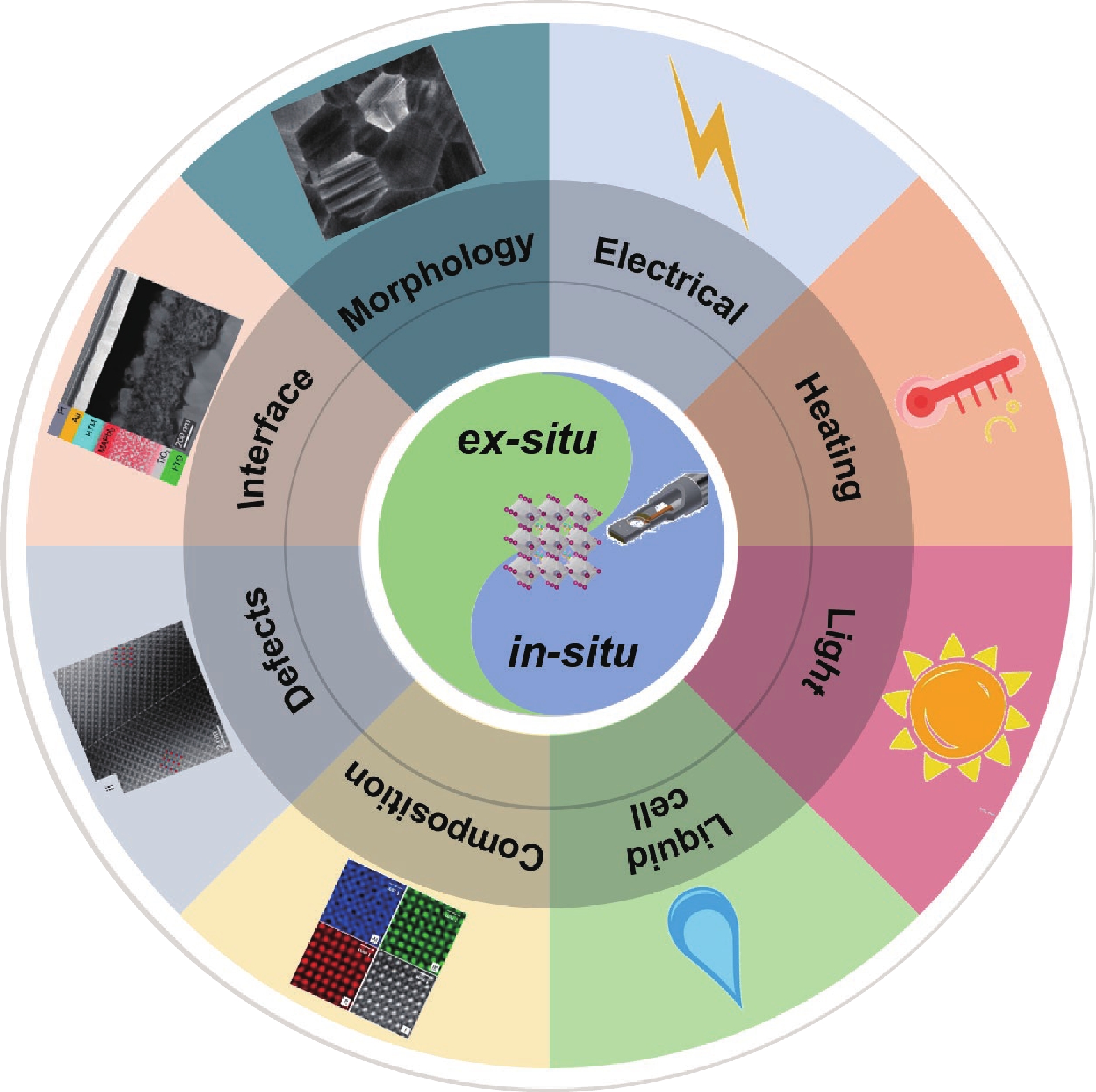
Driven by the urgent need to understand the microstructure–properties relationship for halide perovskites which is strategically important, much effort has been made in the past few years to overcome the difficulty of imaging limited by electron dose, and to further extend the investigation towards operando conditions. This review is therefore dedicated to recent studies of advanced TEM characterizations for halide perovskites. Firstly, the irradiation damage and "artefacts" caused by the interaction of electron beams and perovskites under conventional imaging conditions are summarized and discussed, calling attention to the interpretation of TEM results for this particular materials. Low-dose TEM is then discussed, including conventional technique of electron diffraction and emerging techniques for high-resolution TEM (HRTEM) imaging. Atomic-resolution imaging and defects identification on halide perovskites are reviewed. Composition analysis using energy dispersive X-ray microscopy (EDX) and electron energy loss spectroscopy (EELS) mapping are also discussed. Cryo-TEM for halide perovskites is then given special attention in this review, since it can readily suppress irradiation damage and has been rapidly developed for imaging beam-sensitive energy materials in the past few years. Finally, the applications of in-situ TEM in the degradation study of perovskites under environmental conditions such as heating, biasing, light illumination and humidity are reviewed. An illustration of advanced TEM characterizations for halide perovskites is presented in Fig. 1.
![]()
Figure 1.(Color online) Schematic illustration of advanced TEM characterization for halide perovskites.
2. Irradiation damage on halide perovskites by conventional TEM imaging
The irradiation damage induced by energetic electrons during the imaging of halide perovskites has significantly limited the TEM characterization, and is considered as the cornerstone for the interpretation of as-observed microstructures.
When organic–inorganic hybrid perovskites are imaged using conventional TEM, the structure of the halide perovskites can be destroyed in seconds, resulting in the irradiation damage such as generation of "bubbles" and precipitation of nanoparticles, as shown in Fig. 2. Chen et al. noticed severe damage in the MAPbI3 perovskite polycrystalline film when imaged at a relatively high electron dose of ~9870 e/(Å2·s) (i.e. the dose for obtaining conventional HRTEM images), where nanoparticles precipitated quickly within the irradiated area (Fig. 2(a)). Such irradiation damage was attributed to the electric field generated by the electron beam within the perovskite, and remained by reducing electron dose to 500 e/(Å2·s)[
![]()
Figure 2.(Color online) (a) Electron beam irradiation damage observed in free-standing MAPbI3 films. (i, ii). TEM images recorded initially and after the irradiation (9870 e/(Å2·s) for ~2 min), respectively[
Irradiation damage is also frequently noticed in all-inorganic halide perovskites. Taking CsPbX3 for example, Li et al. found that even short time of exposure could cause "dark spots" to emerge at the corners of the quantum dots (QDs) when imaging CsPbCl3, CsPbBr3 and CsPbI3 QDs as shown in Fig. 2(d)[
More recently, Pb-free halide perovskites with a double perovskite structure are being developed, such as Cs2AgBiBr6, Cs2CuSbCl6, Cs2AgInCl6. Zhou et al. synthesized Cs2CuSbCl6 nanoparticles, and Cruetz et al. synthesized Cs2AgBiCl6, Cs2AgBiBr6 and CsAgBiI6 nanoparticles, and they were all characterized by TEM[
It is generally accepted that the electron dose and dose rate have the most influence on the degradation of halide perovskites under electron irradiation, yet it is interesting to discuss the impact of accelerating voltage, i.e. beam energy. In the damage caused by electron beam radiation, it is generally believed that there are three types of radiation damage mechanisms, that is, knock-on damage, radiolysis, and rise of local temperature caused by phonons excited by electron beam radiation[
3. Degradation mechanism and defects identification of halide perovskite using electron diffraction
Due to the beam-sensitivity of halide perovskites, selected area electron diffraction (SAED) with the advantage of low dose, has become a powerful tool to study the degradation mechanism and intrinsic microstructures of halide perovskites.
Rothmann et al. acquired SAED time-series through continuous irradiation to study the degradation of MAPbI3 single crystal as shown in Fig. 3(a)[
![]()
Figure 3.(Color online) (a) Degradation of MAPbI3 studied using SAED taken from a near-<1
Similar to Rothmann’s work, Chen et al. also studied the degradation process of MAPbI3 through SAED time series[
SAED is also used to study the degradation mechanism of 2D nanosheets due to their extreme beam-sensitivity. Yuan et al. studied the structural changes of BA2FAPb2I7 and BA2MAPb2I7 under electron beam irradiation by recording SAED time series, and proposed the degradation mechanism as following: organic ligands between the nanosheets were firstly destroyed by the electron beam; the organic moieties and [PbBr6] octahedra were then damaged, resulting in the rapid collapse of the structure[
In addition to the study of degradation mechanism, SAED has been employed to characterize the microstructures of halide perovskites in a damage-free manner. Rothmann et al. discovered the existence of nano-twinning in MAPbI3 single crystal by SAED[
4. Emerging TEM approaches for halide perovskites at atomic resolution
Driven by the urgent need to understand the structure-properties relationship of halide perovskites, novel approaches on both hardware and methodology are being developed to overcome the limits opposed by electron dose, and to further push the spatial resolution down to atomic scale.
With regard to the degradation mechanism of halide perovskites under electron irradiation, it is generally accepted that: (1) the electron dose and dose rate are dominating the irradiation process, and therefore low-dose imaging is essential; (2) the disassociation of organic ligands and halide ions is the first to trigger decomposition of halide perovskites. In light of these understandings, various methods have been proposed to push HRTEM imaging of halide perovskites towards atomic scale, including: (1) deposition or coating of carbon film to alleviate the radiolysis damage; (2) improvement on detectors such as direct electron detector to enable ultra-low-dose imaging; (3) developments of low-dose imaging techniques such as exit-wave reconstruction, ptychography, and iDPC etc.
Above-mentioned techniques have demonstrated to be successful in resolving pristine structures of halide perovskites at atomic scale. Yu et al. revealed the microstructure of CsPbBr3 by defocus series at a low dose rate of ~100 e/(Å2·s) under accelerating voltage of 80 kV[
![]()
Figure 4.(Color online) (a) HRTEM of CsPbBr3 nanocrystals (i) where the coexistence of cubic and orthorhombic phases were demonstrated by FFT patterns (ii, iii), simulated diffraction patterns (iv, v), and illustrated structure (vi, vii)[
Thanks to the development of low-dose imaging technique, defects in halide perovskites have been imaged in detail as never before. Cai et al. recently succeeded in imaging grain boundaries of MAPbI3 PSCs at atomic scale by developing a coating approach onto FIB-prepared cross section, as shown in Fig. 4(d)[
5. Chemical mapping of halide perovskites using STEM-EDX or STEM-EELS
Due to the beam sensitivity, elemental mapping of halide perovskites has been a standing issue for microstructure investigations. Large dose is often required to obtain enough counts for either EDX-mapping or EELS-mapping, which exceeds the degradation threshold of halide perovskites. Although chemical mapping has been reported in many halide-perovskites study, it is also known that the instability of halide perovskites during beam irradiation thus leads to the reliability of elemental mapping, questioning whether the mapped results reflect the pristine structure. Therefore, novel approaches have been proposed to enable the elemental mapping down to atomic scale.
Kosasih et al. performed a systematic study on the evaluation of STEM-EDX quality demonstrated on state-of-art triple-cation, double-halide perovskite with a nominal stoichiometry of Cs0.06FA0.79MA0.15Pb(I0.85Br0.15)3[
In order to minimize electron damage, Liu et al. recently fabricated a highly-beam-stable CsPbBr3 nanoplates through an interface-assisted regrowth method using cyanamide[
![]()
Figure 5.(Color online) (a, b) Atomically resolved HAADF-STEM images and corresponding EDX-mappings of CsPbBr3 nanoplates[
On the other hand, STEM-EELS has been demonstrated on orthorhombic CsPbBr3 to determine bandgap as shown in Fig. 5(c)[
6. Fast-developing cryogenic TEM for halide perovskites
Cryogenic TEM (cryo-TEM) has been developed rapidly in recent years. Beyond life science, its development has also offered opportunities to materials science, particularly to those too sensitive for conventional HRTEM and related spectroscopy[
Li et al. combined the cryogenic temperature with direct electron detector dedicated for low-dose imaging, and successfully obtained HRTEM of MAPbI3 and MAPbBr3 under the dose of 12 e/Å2 and 46 e/Å2[
![]()
Figure 6.(Color online) (a) Stacking faults observed in a MAPbI3 with corresponding FFT patterns as inset (i), and corresponding magnified HRTEM (ii, v, vi) with structural model (iii) and (iv) the simulated HRTEM image[
Nevertheless, it should be noted that the use of cryogenic temperature for halide perovskites imaging remains an open issue. It was reported by Rothmann et al. that low temperature could not alleviate irradiation damage but led to rapid amorphization of MAPbI3[
7. In-situ TEM dedicated to reveal degradation of halide perovskites under environmental conditions
Although much progress has been achieved in resolving the microstrure of as-grown halide perovskites or as-fabricated photovoltaic devices from nanoscale down to atomic scale, there is an urgent need to study the structural evolution of halide perovskites based devices under external stimuli such as light, heat and moisture so to understand the degradation of perovskites under environmental factors[
The thermal stability of halide perovskites can be studied byin-situ heating in TEM. As demonstrated by Divitini et al., the morphology and chemical composition change of MAPbI3-based PSC during elavating temperature (up to 250 °C) was monitored using a FIB prepared cross-section (Fig. 7(a))[
![]()
Figure 7.(Color online) (a)
The impact of curent–voltage stimulus on perovskites degradation can be investigated by in-situ biasing. MAPbI3-based PSC was prepared into cross section and subjected to biasing in TEM by Jengros et al.[
Last but not least, the moisture-induced degradation was recently studied using in-operando liquid cell TEM (Fig. 7(c))[
8. Conclusions and perspective
This review summarizes the recent progress of advanced TEM characterization for halide perovskites. The main conclusions are as following.
(1) Due to the presence of halogen ions and organic moieties, halide pervoskites are extremely sensitive to electron beam irradiation. Conventional TEM causes degradation in almost all halide perovskite structures, showing "artifacts" and damage such as the generation and expansion of holes, grain boundary cracking, and nanoparticle precipitation. Although the degradation mechanism under electron beam interaction remains unclear, it generally follows the pathway of "electron beam incidence → organic moieties and/or halogen ion desorption → defect generation and expansion → lattice collapse and amorphization → PbI2 or Pb precipitation". Both electron dose and dose rate have impact on the degradation. The understanding of degradation is essential, as it calls attention to the interpretation of TEM results and ultra-care in performing TEM characterization.
(2) In order to reduce the irradiation damage, low-dose is vital for halide perovskites’ characterization. Electron diffraction has shown to be powerful in resolving the crystal structure and microstructure at low dose. In Table 1–4, we have summarized the imaging conditions as reported in this review according to perovskite chemistry, i.e. MAPbI3, MAPbBr3, all-inorganic CsPbBr3/CsPbI3, and 2D halide perovskites, as an imaging guide for researchers in this field. More importantly, safe dose and damage dose for different perovskite materials are summarized in Fig. 8, where dose limit for imaging is better represented. 2D perovskites are most sensitive to electron dose, whereas MAPbI3 and MAPbBr3 is slightly more robust, and CsPbBr3 has the best tolerance to beam irradiation. It is important to note that dose rate and accelerating voltage also has influence on imaging, and surface treatment to protect the sample can drastically increase the critical dose. Readers are encouraged to refer to the tables and corresponding references for specific notes. Undoubtedly, halide perovskites is one of the most beam-sensitive materials, and researchers are encouraged to carefully design and prepare their TEM experiments in order to achieve meaningful results.
![]()
Figure 8.(Color online) Illustrated summary of safe dose and damage dose for different perovskite materials, plotted in coloured columns. Numbers in the figure correspond to the reference numbers as listed in the tables and references. Shade in each column indicates relatively-safe dose range versus damage-prone dose range. Generally speaking, 2D pvsk is suggested to be imaged below the dose of 50 e/(Å2·s), MAPbI3/ MAPbBr3 below ~100 e/(Å2·s), whereas CsPbBr3 can tolerate dose up to more than 1000 e/(Å2·s).
Table Infomation Is Not EnableTable Infomation Is Not EnableTable Infomation Is Not Enable(3) Emerging techniques have been developed to enable atomic-resolution imaging and chemical mapping of halide pervoskites. Low-dose imaging techniques such as exit-wave reconstruction, LAADF-STEM and ptychography has successfully imaged perovskites at atomic scale. The development of hardware such as direct electron detectors have also succeeded in providing atomically resolved structure of halide perovskites. Additionally, the rapid development of cryo-TEM has emerged as a powerful tool to study the halide perovskites and reveal defects such as grain boundaries and surface steps.
(4) In-situ TEM under heating, biasing and liquid cell is being developed and applied to study the degradation of halide perovskites under operando conditions. Microstructural change has been revealed with unprecedented details.
Thanks to the rapid developments of emerging TEM techniques, halide perovskites have been resolved down to atomic scale with unprecedented details. Perspectives of TEM characterizations for halide perovskites are proposed as following:
(1) Sample preparation. Imaging techniques such as iDPC, ptychography, and the developments of detectors have paved ways for low-dose imaging, but the bottleneck is sample preparation, particularly for PSC thin films. Conventionally, FIB is used to prepare cross sections, but beam damage of Ga+ ions can induce significant damage to the sample prior to imaging. The use of cryo-FIB and surface passivation has shown their advantages in alleviating beam damage, and more studies are encouraged.
(2) Development of emerging techniques. Although low-dose imaging and in-situ TEM has been demonstrated to reveal the structure-property relationship, the studies are still limited to a few examples. More investigations on different materials and devices are expected.
(3) Interpretation of TEM data. Degradation mechanism has been discussed in this review, emphasizing the impact of electron dose/dose rate on halide perovskite structure. It is clear that only low dose imaging can reveal the halide perovskite structure, although conventional TEM imaging and EDX/EELS study involves large dose, which significantly exceeds damage threshold. Therefore, we call attentions to the interpretation of TEM data as reported in literatures, where attentions should be paid to the imaging condition before correlation to the conclusions.
Halide perovskites are strategically important in the field of energy materials. Along with the rapid development of the materials and related devices, there is an urgent need to understand the structure-property relationship from nanoscale to atomic scale. Much effort has been made in the past few years to address the beam-sensitivity of this particular materials, and more applications of emerging TEM characterizations are foreseen in the coming future, unveiling the structural origin of halide perovskite’s unique properties and degradation mechanism under operando conditions, so to assist the design of a more efficient and robust energy material.
Acknowledgements
X.K. and M.S. acknowledge the Beijing Municipal High Level Innovative Team Building Program (IDHT20190503) and the National Natural Science Fund for Innovative Research Groups of China (51621003). X.W. and X.K. acknowledge the National Natural Science Foundation of China (12074017).
References
[1] Q Jiang, Y Zhao, X W Zhang et al. Surface passivation of perovskite film for efficient solar cells. Nat Photonics, 13, 460(2019).
[2] Y W Lin, G M Lin, B Y Sun et al. Nanocrystalline perovskite hybrid photodetectors with high performance in almost every figure of merit. Adv Funct Mater, 28, 1705589(2018).
[3] J H Ran, O Dyck, X Z Wang et al. Electron-beam-related studies of halide perovskites: Challenges and opportunities. Adv Energy Mater, 10, 1903191(2020).
[4] P F Chen, W J Ong, Z H Shi et al. Pb-based halide perovskites: Recent advances in photo(electro)catalytic applications and looking beyond. Adv Funct Mater, 30, 1909667(2020).
[5] T Ye, L Pan, Y Yang et al. Synthesis of highly-oriented black CsPbI3 microstructures for high-performance solar cells. Chem Mater, 32, 3235(2020).
[6] M A Green, A Ho-Baillie, H J Snaith. The emergence of perovskite solar cells. Nat Photonics, 8, 506(2014).
[7] Q Dong, Y Fang, Y Shao et al. Electron-hole diffusion lengths > 175 μm in solution-grown CH 3NH3PbI3 single crystals. Science, 347, 967(2015).
[8] Z J Shi, J Guo, Y H Chen et al. Lead-free organic-inorganic hybrid perovskites for photovoltaic applications: Recent advances and perspectives. Adv Mater, 29, 1605005(2017).
[9] Z B Yang, A Rajagopal, A K Y Jen. Ideal bandgap organic–inorganic hybrid perovskite solar cells. Adv Mater, 29, 1704418(2017).
[10] M Kim, J Jeong, H Z Lu et al. Conformal quantum dot–SnO2 layers as electron transporters for efficient perovskite solar cells. Science, 375, 302(2022).
[11] C Liu, J Sun, W L Tan et al. Alkali cation doping for improving the structural stability of 2D perovskite in 3D/2D PSCs. Nano Lett, 20, 1240(2020).
[12] F X Xie, C C Chen, Y Z Wu et al. Vertical recrystallization for highly efficient and stable formamidinium-based inverted-structure perovskite solar cells. Energy Environ Sci, 10, 1942(2017).
[13] W C Xiang, Z W Wang, D J Kubicki et al. Europium-doped CsPbI2Br for stable and highly efficient inorganic perovskite solar cells. Joule, 3, 205(2019).
[14] S Yang, W X Niu, A L Wang et al. Ultrathin two-dimensional organic-inorganic hybrid perovskite nanosheets with bright, tunable photoluminescence and high stability. Angew Chem Int Ed, 56, 4252(2017).
[15] Y Sun, Y Yin, M Pols et al. Engineering the phases and heterostructures of ultrathin hybrid perovskite nanosheets. Adv Mater, 32, 2002392(2020).
[16] Y Su, X J Chen, W Y Ji et al. Highly controllable and efficient synthesis of mixed-halide CsPbX3 (X = Cl, Br, I) perovskite QDs toward the tunability of entire visible light. ACS Appl Mater Interfaces, 9, 33020(2017).
[17] H Utzat, W W Sun, A E K Kaplan et al. Coherent single-photon emission from colloidal lead halide perovskite quantum dots. Science, 363, 1068(2019).
[18] M R Filip, S Hillman, A A Haghighirad et al. Band gaps of the lead-free halide double perovskites Cs2BiAgCl6 and Cs2BiAgBr6 from theory and experiment. J Phys Chem Lett, 7, 2579(2016).
[19] H X Zhong, M Yang, G Tang et al. Type-II lateral heterostructures of monolayer halide double perovskites for optoelectronic applications. ACS Energy Lett, 5, 2275(2020).
[20] E T McClure, M R Ball, W Windl et al. Cs2AgBiX6 (X = Br, Cl): New visible light absorbing, lead-free halide perovskite semiconductors. Chem Mater, 28, 1348(2016).
[21] C C Wu, Q H Zhang, Y Liu et al. The dawn of lead-free perovskite solar cell: Highly stable double perovskite Cs2AgBiBr6 film. Adv Sci, 5, 1700759(2018).
[22] G Volonakis, A A Haghighirad, R L Milot et al. Cs2InAgCl6: A new lead-free halide double perovskite with direct band gap. J Phys Chem Lett, 8, 772(2017).
[23] Z Z Li, W J Yin. Recent progress in Pb-free stable inorganic double halide perovskites. J Semicond, 39, 071003(2018).
[24] Z W Xiao, Y F Yan. Progress in theoretical study of metal halide perovskite solar cell materials. Adv Energy Mater, 7, 1701136(2017).
[25] Y Yang, Y B Sun, Y S Jiang. Structure and photocatalytic property of perovskite and perovskite-related compounds. Mater Chem Phys, 96, 234(2006).
[26] H Zhang, X Fu, Y Tang et al. Phase segregation due to ion migration in all-inorganic mixed-halide perovskite nanocrystals. Nat Commun, 10, 1088(2019).
[27] B Y Huang, Z H Liu, C W Wu et al. Polar or nonpolar? That is not the question for perovskite solar cells.. Natl Sci Rev, 8, nwab094(2021).
[28] Y T Lei, Y K Xu, M Wang et al. Origin, influence, and countermeasures of defects in perovskite solar cells. Small, 17, 2005495(2021).
[29] J P Wu, S C Liu, Z B Li et al. Strain in perovskite solar cells: Origins, impacts and regulation. Natl Sci Rev, 8, nwab047(2021).
[30] C K Sin, J Z Zhang, K Tse et al. A brief review of formation energies calculation of surfaces and edges in semiconductors. J Semicond, 41, 061101(2020).
[31] S Bhattacharya, G K Chandra, P Predeep. A microstructural analysis of 2D halide perovskites: Stability and functionality. Front Nanotechnol, 3, 657948(2021).
[32] T W Kim, N G Park. Methodologies for structural investigations of organic lead halide perovskites. Mater Today, 38, 67(2020).
[33] V Kumar, M Nisika. Temporal-spatial-energy resolved advance multidimensional techniques to probe photovoltaic materials from atomistic viewpoint for next-generation energy solutions. Energy Environ Sci, 14, 4760(2021).
[34] J J Liu. Advances and applications of atomic-resolution scanning transmission electron microscopy. Microsc Microan, 27, 943(2021).
[35] S M Ribet, A A Murthy, E W Roth et al. Making the most of your electrons: Challenges and opportunities in characterizing hybrid interfaces with STEM. Mater Today, 50, 100(2021).
[36] F X Zha, Q Y Zhang, H G Dai et al. The scanning tunneling microscopy and spectroscopy of GaSb1–
[37] Z Yang, S Z Liu. Perspective on the imaging device based on perovskite materials. J Semicond, 41, 050401(2020).
[38] M U Rothmann, W Li, Y Zhu et al. Direct observation of intrinsic twin domains in tetragonal CH3NH3PbI3. Nat Commun, 8, 14547(2017).
[39] D L Zhang, Y H Zhu, L M Liu et al. Atomic-resolution transmission electron microscopy of electron beam-sensitive crystalline materials. Science, 359, 675(2018).
[40] Y Zhu, S Wang, B Li et al. Twist-to-untwist evolution and cation polarization behavior of hybrid halide perovskite nanoplatelets revealed by cryogenic transmission electron microscopy. J Phys Chem Lett, 12, 12187-95(2021).
[41] Y Yu, D D Zhang, C Kisielowski et al. Atomic resolution imaging of halide perovskites. Nano Lett, 16, 7530(2016).
[42] G Divitini, S Cacovich, F Matteocci et al.
[43] Y H Seo, J H Kim, D H Kim et al.
[44] Y Ge, X L Mu, Y Lu et al. Photoinduced degradation of lead halide perovskite thin films in air. Acta Phys Chim Sin, 36, 1905039(2020).
[45] M U Rothmann, W Li, J Etheridge et al. Microstructural characterisations of perovskite solar cells - from grains to interfaces: Techniques, features, and challenges. Adv Energy Mater, 7, 1700912(2017).
[46] M U Rothmann, W Li, Y Zhu et al. Structural and chemical changes to CH3NH3PbI3 induced by electron and gallium ion beams. Adv Mater, 30, 1800629(2018).
[47] X Y Chen, Z W Wang. Investigating chemical and structural instabilities of lead halide perovskite induced by electron beam irradiation. Micron, 116, 73(2019).
[48] Y B Li, W J Zhou, Y Z Li et al. Unravelling degradation mechanisms and atomic structure of organic-inorganic halide perovskites by cryo-EM. Joule, 3, 2854(2019).
[49] T W Kim, T Kondo. Direction-selective electron beam damage to CH3NH3PbI3 based on crystallographic anisotropy. Appl Phys Express, 13, 091001(2020).
[50] A Alberti, C Bongiorno, E Smecca et al. Pb clustering and PbI2 nanofragmentation during methylammonium lead iodide perovskite degradation. Nat Commun, 10, 2196(2019).
[51] A Manekkathodi, A Marzouk, J Ponraj et al. Observation of structural phase transitions and PbI2 formation during the degradation of triple-cation double-halide perovskites. ACS Appl Energy Mater, 3, 6302(2020).
[52] L T Dou, A B Wong, Y Yu et al. Atomically thin two-dimensional organic-inorganic hybrid perovskites. Science, 349, 1518(2015).
[53] L F Nie, X X Ke, M L Sui. Microstructural study of two-dimensional organic-inorganic hybrid perovskite nanosheet degradation under illumination. Nanomaterials, 9, 722(2019).
[54] F Li, Y Liu, H Wang et al. Postsynthetic surface trap removal of CsPbX3 (X = Cl, Br, or I) quantum dots via a ZnX2/hexane solution toward an enhanced luminescence quantum yield. Chem Mater, 30, 8546(2018).
[55] G D Su, B L He, Z K Gong et al. Enhanced charge extraction in carbon-based all-inorganic CsPbBr3 perovskite solar cells by dual-function interface engineering. Electrochim Acta, 328, 135102(2019).
[56] Z Y Dang, J Shamsi, F Palazon et al.
[57] S H Zou, C P Liu, R F Li et al. From nonluminescent to blue-emitting Cs4PbBr6 nanocrystals: Tailoring the insulator bandgap of 0D perovskite through Sn cation doping. Adv Mater, 31, 1900606(2019).
[58] T Wang, Z Yang, L Yang et al. Atomic-scale insights into the dynamics of growth and degradation of all-inorganic perovskite nanocrystals. J Phys Chem Lett, 11, 4618(2020).
[59] H Funk, O Shargaieva, A Eljarrat et al.
[60] W Zhou, P Han, X Zhang et al. Lead-free small-bandgap Cs2CuSbCl6 double perovskite nanocrystals. J Phys Chem Lett, 11, 6463(2020).
[61] S E Creutz, E N Crites, M C de Siena et al. Colloidal nanocrystals of lead-free double-perovskite (elpasolite) semiconductors: Synthesis and anion exchange to access new materials. Nano Lett, 18, 1118(2018).
[62] Y H Feng, X X Ke, M L Sui. Effect of electron irradiation on inorganic double perovskite solar cell material Cs2AgBiBr6. J Chin Electron Microsc Soc, 39, 1(2020).
[63] R F Egerton, P Li, M Malac. Radiation damage in the TEM and SEM. Micron, 35, 399(2004).
[64] Z L Gong, Y Yang. The application of synchrotron X-ray techniques to the study of rechargeable batteries. J Energy Chem, 27, 1566(2018).
[65] Z H Cai, Y N Wu, S Y Chen. Energy-dependent knock-on damage of organic-inorganic hybrid perovskites under electron beam irradiation: First-principles insights. Appl Phys Lett, 119, 123901(2021).
[66] Z X Chen, X X Ke, L J Zhu et al. Electron microscopy of organic-inorganic hybrid perovskite solar cell materials: degradation mechanism study and imaging condition optimization. J Chin Electron Microsc Soc, 38, 15(2019).
[67] M U Rothmann, J S Kim, J Borchert et al. Atomic-scale microstructure of metal halide perovskite. Science, 370, 6516(2020).
[68] S Chen, X Zhang, J Zhao et al. Atomic scale insights into structure instability and decomposition pathway of methylammonium lead iodide perovskite. Nat Commun, 9, 4807(2018).
[69] S L Chen, Y Zhang, X W Zhang et al. General decomposition pathway of organic-inorganic hybrid perovskites through an intermediate superstructure and its suppression mechanism. Adv Mater, 32, 2001107(2020).
[70] S L Chen, P Gao. Challenges, myths, and opportunities of electron microscopy on halide perovskites. J Appl Phys, 128, 010901(2020).
[71] S L Chen, Y Zhang, J J Zhao et al. Transmission electron microscopy of organic-inorganic hybrid perovskites: Myths and truths. Sci Bull, 65, 1643(2020).
[72] X G Zhou, C Q Yang, X Sang et al. Probing the electron beam-induced structural evolution of halide perovskite thin films by scanning transmission electron microscopy. J Phys Chem C, 125, 10786(2021).
[73] B Yuan, E Z Shi, C Liang et al. Structural damage of two-dimensional organic–inorganic halide perovskites. Inorganics, 8, 13(2020).
[74] W Li, M U Rothmann, Y Zhu et al. The critical role of composition-dependent intragrain planar defects in the performance of MA1–
[75] Y Gao, E Shi, S Deng et al. Molecular engineering of organic–inorganic hybrid perovskites quantum wells. Nat Chem, 11, 1151(2019).
[76] W Pan, H Wu, J Luo et al. Cs2AgBiBr6 single-crystal X-ray detectors with a low detection limit. Nat Photonics, 11, 726(2017).
[77] J Luo, X Wang, S Li et al. Efficient and stable emission of warm-white light from lead-free halide double perovskites. Nature, 563, 541(2018).
[78] H T Pham, Y T Yin, G Andersson et al. Unraveling the influence of CsCl/MACl on the formation of nanotwins, stacking faults and cubic supercell structure in FA-based perovskite solar cells. Nano Energy, 87, 106226(2021).
[79] T A S Doherty, S Nagane, D J Kubicki et al. Stabilized tilted-octahedra halide perovskites inhibit local formation of performance-limiting phases. Science, 374, 1598(2021).
[80] M C Brennan, M Kuno, S Rouvimov. Crystal structure of individual CsPbBr3 perovskite nanocubes. Inorg Chem, 58, 1555(2019).
[81] K P Song, L M Liu, D L Zhang et al. Atomic-resolution imaging of halide perovskites using electron microscopy. Adv Energy Mater, 10, 1904006(2020).
[82] S Chen, C Wu, B Han et al. Atomic-scale imaging of CH3NH3PbI3 structure and its decomposition pathway. Nat Commun, 12, 5516(2021).
[83] G Y Qiao, D H Guan, S Yuan et al. Perovskite quantum dots encapsulated in a mesoporous metal-organic framework as synergistic photocathode materials. J Am Chem Soc, 143, 14253(2021).
[84] R dos Reis, H Yang, C Ophus et al. Determination of the structural phase and octahedral rotation angle in halide perovskites. Appl Phys Lett, 112, 071901(2018).
[85] E J VandenBussche, C P Clark, R J Holmes et al. Mitigating damage to hybrid perovskites using pulsed-beam TEM. ACS Omega, 5, 31867(2020).
[86] S H Cai, J Dai, Z P Shao et al. Atomically resolved electrically active intragrain interfaces in perovskite semiconductors. J Am Chem Soc, 144, 1910(2022).
[87] E Shi, B Yuan, S B Shiring et al. Two-dimensional halide perovskite lateral epitaxial heterostructures. Nature, 580, 614(2020).
[88] H J Jung, C C Stompus, M G Kanatzidis et al. Self-passivation of 2D ruddlesden–popper perovskite by polytypic surface PbI2 encapsulation. Nano Lett, 19, 6109(2019).
[89] Y Yu, D D Zhang, P D Yang. Ruddlesden-popper phase in two-dimensional inorganic halide perovskites: A plausible model and the supporting observations. Nano Lett, 17, 5489(2017).
[90] Z Y Dang, B Dhanabalan, A Castelli et al. Temperature-driven transformation of CsPbBr3 nanoplatelets into mosaic nanotiles in solution through self-assembly. Nano Lett, 20, 1808(2020).
[91] F U Kosasih, S Cacovich, G Divitini et al. Nanometric chemical analysis of beam-sensitive materials: A case study of STEM-EDX on perovskite solar cells. Small Methods, 5, 2000835(2021).
[92] J Liu, K Song, X Zheng et al. Cyanamide passivation enables robust elemental imaging of metal halide perovskites at atomic resolution. J Phys Chem Lett, 12, 10402(2021).
[93] R Brescia, S Toso, Q Ramasse et al. Bandgap determination from individual orthorhombic thin cesium lead bromide nanosheets by electron energy-loss spectroscopy. Nanoscale Horiz, 5, 1610(2020).
[94] Y B Li, W Huang, Y Z Li et al. Opportunities for cryogenic electron microscopy in materials science and nanoscience. ACS Nano, 14, 9263(2020).
[95] Z W Zhang, Y Cui, R Vila et al. Cryogenic electron microscopy for energy materials. Acc Chem Res, 54, 3505(2021).
[96] Y M Zhu, Z G Gui, Q Wang et al. Direct atomic scale characterization of the surface structure and planar defects in the organic-inorganic hybrid CH3NH3PbI3 by Cryo-TEM. Nano Energy, 73, 104820(2020).
[97] Y M Zhu, Q Zhang, X M Yang et al. Probing atomic structure of beam-sensitive energy materials in their native states using cryogenic transmission electron microscopes. iScience, 24, 103385(2021).
[98] Z Y Dang, J Shamsi, Q A Akkerman et al. Low-temperature electron beam-induced transformations of cesium lead halide perovskite nanocrystals. ACS Omega, 2, 5660(2017).
[99] N A Rivas, A Babayigit, B Conings et al. Cryo-focused ion beam preparation of perovskite based solar cells for atom probe tomography. PLoS One, 15, e0227920(2020).
[100] J F Zhou, N N Wei, D L Zhang et al. Cryogenic focused ion beam enables atomic-resolution imaging of local structures in highly sensitive bulk crystals and devices. J Am Chem Soc, 144, 3182(2022).
[101] J W Lee, S Seo, P Nandi et al. Dynamic structural property of organic-inorganic metal halide perovskite. iScience, 24, 101959(2021).
[102] S D Stranks. Multimodal microscopy characterization of halide perovskite semiconductors: Revealing a new world (dis)order. Matter, 4, 3852(2021).
[103] S Thampy, W J Xu, J W P Hsu. Metal oxide-induced instability and its mitigation in halide perovskite solar cells. J Phys Chem Lett, 12, 8495(2021).
[104] C C Zhang, S Yuan, Y H Lou et al. Physical fields manipulation for high-performance perovskite photovoltaics. Small, 2107556(2022).
[105] F U Kosasih, C Ducati. Characterising degradation of perovskite solar cells through
[106] S Kundu, T L Kelly.
[107] F McGrath, U V Ghorpade, K M Ryan. Synthesis and dimensional control of CsPbBr3 perovskite nanocrystals using phosphorous based ligands. J Chem Phys, 152, 174702(2020).
[108] Q Jeangros, M Duchamp, J Werner et al.
[109] H J Jung, D Kim, S Kim et al. Stability of halide perovskite solar cell devices:
[110] M C Kim, N Ahn, D Y Cheng et al. Imaging real-time amorphization of hybrid perovskite solar cells under electrical biasing. ACS Energy Lett, 6, 3530(2021).
[111] C Zhang, J F S Fernando, K L Firestein et al. Crystallography-derived optoelectronic and photovoltaic properties of CsPbBr3 perovskite single crystals as revealed by
[112] M A Akhavan Kazemi, P Raval, K Cherednichekno et al. Molecular-level insight into correlation between surface defects and stability of methylammonium lead halide perovskite under controlled humidity. Small Methods, 5, 2000834(2021).
[113] F Y Qin, Z W Wang, Z L Wang. Anomalous growth and coalescence dynamics of hybrid perovskite nanoparticles observed by liquid-cell transmission electron microscopy. ACS Nano, 10, 9787(2016).

Set citation alerts for the article
Please enter your email address
© Copyright 2018-2021 | Chinese Laser Press. All Rights Reserved 沪ICP备15018463号-20