• Journal of Semiconductors
  • Vol. 43, Issue 4, 041101 (2022)
Sai Jiang1, Qinyong Dai2, Jianhang Guo2, and Yun Li2
Author Affiliations
  • 1School of Microelectronics and Control Engineering, Changzhou University, Changzhou 213164, China
  • 2National Laboratory of Solid-State Microstructures, School of Electronic Science and Engineering, Collaborative Innovation Center of Advanced Microstructures, Nanjing University, Nanjing 210093, China
  • show less
    DOI: 10.1088/1674-4926/43/4/041101 Cite this Article
    Sai Jiang, Qinyong Dai, Jianhang Guo, Yun Li. In-situ/operando characterization techniques for organic semiconductors and devices[J]. Journal of Semiconductors, 2022, 43(4): 041101 Copy Citation Text show less

    Abstract

    The increasing demands of multifunctional organic electronics require advanced organic semiconducting materials to be developed and significant improvements to be made to device performance. Thus, it is necessary to gain an in-depth understanding of the film growth process, electronic states, and dynamic structure-property relationship under realistic operation conditions, which can be obtained by in-situ/operando characterization techniques for organic devices. Here, the up-to-date developments in the in-situ/operando optical, scanning probe microscopy, and spectroscopy techniques that are employed for studies of film morphological evolution, crystal structures, semiconductor-electrolyte interface properties, and charge carrier dynamics are described and summarized. These advanced technologies leverage the traditional static characterizations into an in-situ and interactive manipulation of organic semiconducting films and devices without sacrificing the resolution, which facilitates the exploration of the intrinsic structure-property relationship of organic materials and the optimization of organic devices for advanced applications.

    1. Introduction

    Since the discovery of the semiconducting nature of polythiophene, organic electronics have experienced tremendous development[1]. In particular, organic field-effect transistors (OFETs), light-emitting diodes (OLEDs), and photovoltaic cells (OPVs) are key candidates for next generation of electronics and optoelectronics, thus revolutionizing the information, photonics, and energy sciences[28]. Recently, the electrical and optoelectrical performance of OFETs, OLEDs, and OPVs have improved impressively, due to new molecular design strategies, improved process engineering, effective interface optimization, and advanced device architecture[4, 913]. However, despite these remarkable advances, as a new research topic, organic devices still face some key challenges, as follows: (i) the important aspects of packing motifs and growth strategies of organic semiconducting films for high-performance applications are still difficult; (ii) the relationship between charge-transport physics and the molecular structure properties is not fully understood; and (iii) an in-depth understanding of electrode, dielectric, and interface properties under various device structures and operating circumstances is still lacking.

    To solve these issues, it is important to utilize more advanced characterization techniques. Note that in-situ/operando techniques for studying organic semiconductors have been developed as powerful tools to achieve unprecedented insights into complex film growth, electronic states, and structure-property relationships under conditions relevant to device operation or device manipulation[1423], which cannot be revealed by common ex-situ measurements. Hence, in-situ/operando techniques can contribute to our understanding of the nature of molecular assembly mechanisms and intrinsic electronic properties, which can further improve molecular design and device performance.

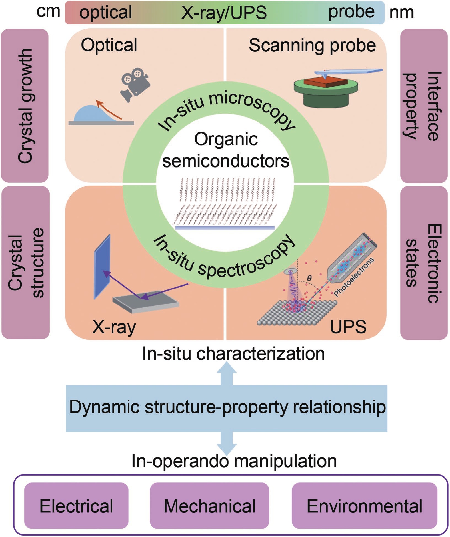
    In this review, recent advances in the application of in-situ/operando techniques for the characterizations of organic semiconductors and devices are thoroughly summarized (Fig. 1). First, we focus on a variety of in-situ/operando optical and scanning probe microscopy for real-time observation of organic film crystallization, as well as characterization of local morphologies, electron/ion coupling, and semiconductor/electrolyte interface of organic devices with unprecedented resolution in complex solid/liquid environments. Then, we provide an introduction to in-situ spectroscopy techniques, including X-ray characterization techniques and ultraviolet photoelectron spectroscopy (UPS), to probe the crystal structures and electronic states of organic devices in-operando. These complementary in-situ techniques are beneficial to the study of the dynamic structure-property relationships, from centimeter to nanometer scales. Finally, challenges and outlooks for developing in-situ/operando techniques in organic semiconductors are discussed. Therefore, this review provides not only an overview of growth mechanisms and electronic properties of organic semiconductors but it also highlights the elegant in-situ/operando analytical methods that have helped to elucidate these mechanisms for more in-depth physics of organic electronics.

    (Color online) Overview of various in-situ characterization techniques with different resolutions, from centimeter to nanometer, to study the dynamic structure-property relationship under manipulation.

    Figure 1.(Color online) Overview of various in-situ characterization techniques with different resolutions, from centimeter to nanometer, to study the dynamic structure-property relationship under manipulation.

    2. In-situ/operando microscopy techniques

    Organic semiconductors are assembled via weak noncovalent bonding among conjugated molecules, such as π–π interactions and van der Waals forces, leading to the important nature of self-assembly and multiple charge-transport mechanisms between molecules[8, 24, 25]. The morphology, molecular packing structure, and charge carrier dynamics of organic films and crystals, which are commonly prepared by vapor-grown methods and solution-based approaches, are diverse and complicated thanks to the complex interdependence of experimental parameters[10, 11, 26, 27]. Hence, it is important to unveil the physical process and electronic states underlying various growth mechanisms and device structures using in-situ/operando techniques for precise control of thin-film morphology and performance, which is critical in studying intrinsic material properties and advanced electronic applications. Considering the stability property of organic crystalline films, in-situ characterization techniques to study the growth process and dynamic of molecular assembly should be noninvasive, such as in-situ optical and scanning probe microscopy, while scanning electron microscopy (SEM) or transmission electron microscope (TEM) are normally considered to be destructive to organic thin films because they use a high-power electron beam. In the following section, we briefly introduce in-situ optical and scanning probe microscopy to study the structure and interface properties of organic films and devices.

    2.1. In-situ optical microscopy

    Achieving high-quality organic crystalline films in large sizes is important to improve the electrical performance of organic devices. Considering the adjustments in molecular structures and deposition parameters, solution-based coating methods (e.g., drop-casting, spin-coating, bar-coating, solution-shearing, and floating-coffee-ring-driven-assembly) offer great potential to obtain organic crystals with large-area scalability, high morphological uniformity, and perfect crystalline order[10, 26, 28, 29]. In contrast to vacuum deposition, solution-based coating is dependent on the fluid dynamics in the liquid-substrate interface[30], which is difficult to capture and manipulate at the hundreds of nanometer to micrometer scales. Numerical simulations have previously been developed to study the fluid flow process in the meniscus geometry with multiple parameters[3133]. However, the limited computation domains, simplified two-dimensional (2D) flow model, and various processing variables result in deviation from the actual crystallization process. To overcome these limitations, in-situ optical microscopy, as a non-destructive characterization method, can intuitively reproduce the growth process on a small scale in real time[22, 34].

    Recently, Leeet al. used in-situ optical microscopy to observe the crystallization process of TIPS-pentacene thin films using a continuous-flow microfluidic-channel-based meniscus-guided coating (CoMiC)[22], which could precisely manipulate the flow behavior via microfluidic channels (Figs. 2(a) and 2(b)). Based on the in-situ characterization and numerical simulation, the relationship between flow pattern, thin-film crystallization, and electrical performance of OFETs is comprehensively analyzed and reveals that chaotic advection leads to device-to-device uniformity. This work provides effective strategies to tune solution-based crystallization properties for performance optimization of OFETs, solar cells, and displays. Furthermore, top-view and side-view in-situ high-speed optical microscopies were used to obtain three-dimensional (3D) meniscus geometry under multiple experimental conditions during solution shearing (Fig. 2(c))[34]. The top-, side-, and 3D-view microscopies for the visualization of the contact line/crystallization process and cross-sectional meniscus shape are shown in Fig. 2(d), contributing to the mathematical model for mass and momentum transport within the meniscus geometry. Therefore, in-situ high-speed optical microscopy enables the analysis and prediction of the crystallization process of organic films under multiple experimental parameters. This technique will be highly useful and broadly applicable to various materials and coating systems for an in-depth understanding of thin-film growth phenomena and optimization of device performance.

    (Color online) In-situ optical microscopy for characterizations of organic crystalline films. (a) Schematic diagram of CoMiC-based analytical system along the entire flow path connecting flow pattern, crystallization, and thin-film properties (upper panel of (a)). Side-view in-situ image analysis of meniscus shape variation during the coating (lower panel of (a)). (b) In-situ microscopy images showing the variation of solution/thin-film boundary and crystallization process of doped TIPS-pentacene using the FM-CoMiC and the SHM-CoMiC[22]. (c) Schematic diagram of top-view and side-view in-situ microscopy to investigate the relationship between 3D meniscus geometry and crystallization during solution shearing. (d) The top-, side-, and 3D-view microscopies for the visualization of the contact line/crystallization process and cross-sectional meniscus shape[34].

    Figure 2.(Color online) In-situ optical microscopy for characterizations of organic crystalline films. (a) Schematic diagram of CoMiC-based analytical system along the entire flow path connecting flow pattern, crystallization, and thin-film properties (upper panel of (a)). Side-view in-situ image analysis of meniscus shape variation during the coating (lower panel of (a)). (b) In-situ microscopy images showing the variation of solution/thin-film boundary and crystallization process of doped TIPS-pentacene using the FM-CoMiC and the SHM-CoMiC[22]. (c) Schematic diagram of top-view and side-view in-situ microscopy to investigate the relationship between 3D meniscus geometry and crystallization during solution shearing. (d) The top-, side-, and 3D-view microscopies for the visualization of the contact line/crystallization process and cross-sectional meniscus shape[34].

    2.2. In-situ scanning probe microscopy

    2.2.1. In-situ atomic force microscopy (AFM)

    Non-contact in-situ optical microscopy can quickly characterize the kinetic process of solution-based crystallization of organic semiconducting films at the micrometer scale in real time of a few milliseconds; however, the large-scale property limits the observation of molecule assembling dynamics with nanometer resolution. In particular, it is still difficult to capture the moments of the assembling process of organic crystals on a local scale in real time. Although conventional X-ray diffraction (XRD) analyses have been used to study the molecular structure revolution, which only provide spatially and time-averaged structure transformation from the reciprocal diffraction data[21]. Hence, in-situ AFM, as one of the promising scanning probe techniques, can directly characterize the crystal growth with much higher resolution and at time scale of several seconds[16, 17, 20, 3537]. More importantly, no high vacuum and high-energy electron beams are required in AFM to guarantee a non-destructive method for organic films, in contrast to electron microscopy techniques.

    Recently, using real-time in-situ AFM, Chenet al. successfully imaged the entire self-assembly processes and the kinetics of crystalline films from amorphous solid states at the minute timescale[38]. As shown in Fig. 3(a), AFM images of the single-crystal film that evolved over time revealed that the growth processes consisted of five distinct steps: droplet flattening, film coalescence, spinodal decomposition, Ostwald ripening, and self-reorganized layer growth. This growth method contributed to high-quality microwire arrays.

    (Color online) In-situ AFM characterizations. (a) Evolutionary selection growth approach and time-lapse sequence of representative AFM images showing the morphological evolution of the precursors on the SiO2 surface. Scale bar: 2 μm[38]. (b) Schematic illustration of the experimental setup for in-situ AFM imaging with perfusion flow of the guest solution. (c) 1.0 × 1.0 µm2 topographic images of the PCP surface taken at the indicated times under the perfusion flow of a 200 mM bpy solution with a constant flow rate. The high-resolution parts are 30 × 30 nm2 phase images of the liquid–solid interface taken at lattice scale[21].

    Figure 3.(Color online) In-situ AFM characterizations. (a) Evolutionary selection growth approach and time-lapse sequence of representative AFM images showing the morphological evolution of the precursors on the SiO2 surface. Scale bar: 2 μm[38]. (b) Schematic illustration of the experimental setup for in-situ AFM imaging with perfusion flow of the guest solution. (c) 1.0 × 1.0  µm2 topographic images of the PCP surface taken at the indicated times under the perfusion flow of a 200 mM bpy solution with a constant flow rate. The high-resolution parts are 30 × 30 nm2 phase images of the liquid–solid interface taken at lattice scale[21].

    Note that the molecule assembly of solution-based techniques for organic crystals occurs at the liquid/solid interface, which is difficult to access by conventional optical and electron microscopies[21]. In-situ liquid-phase AFM with crystal lattice-scale resolution provides a platform to observe crystalline surfaces in the liquid phase in a ‘live’ state (Fig. 3(b)). As shown in Fig. 3(c), Hosono et al. utilized the liquid-phase AFM to capture lattice transition and molecular dynamics of single-crystalline porous coordination polymers (PCP) in flowing solution taken at lattice scale[21]. It was found that bulk PCP crystals underwent reversible structural transformations in response to the presence of guest molecules. In addition, layer-by-layer delamination processes were obtained in-situ and indicated the inherent structural fluidity of the single-crystalline PCP surface. Therefore, these works of in-situ AFM demonstrate the advantages of real-time and real-space observations of the local surface structures of organic films, which offer us an in-depth understanding of the growth mechanism for further morphology optimizations of high-performance organic films.

    2.2.2. In-situ probe microscopy with advanced functions

    The ability to probe electrical and electrochemical properties of organic semiconducting films in contact with a liquid solution during device operation is important because it can reveal real-time film crystallization, defects, and charge carrier transport properties for further performance optimization[5, 20, 3944]. However, the interface of semiconductor/liquid limits the in-situ/operando characterization of local electrical properties, such as carrier density, mobility, and interfacial potential, which are not accessible by Kelvin probe force microscopy (KPFM) operated in air. Therefore, in-situ liquid-phase probe microscopies with advanced functions, such as in-situ electrochemical strain microscopy (ESM) and scanning dielectric microscopy (SDM), are able to characterize the local electronic and strain properties of organic semiconducting films in a complex liquid-phase environment[20, 37].

    With the development of organic electronics, the coupling of organic semiconductors with biology is an emerging and continuously growing field for many advanced applications, such as molecular sensing, cell culture analysis, medical diagnostics, and synapses for neuromorphic computing[4550]. Among these applications, electrolyte-gated organic field-effect transistors (EGOFETs) and organic electrochemical transistors (OECTs) have emerged as promising devices in organic bioelectronics[5, 16, 44, 5153]. As shown in Fig. 4(a), in OECTs and EGOFETs, the dielectric is replaced by a liquid-phase electrolyte. Note that, in OECTs, ions from the electrolyte can penetrate the whole bulk of the polymeric channel, while EGOFETs are driven by the field-effect without ion uptake response[54]. In these devices, in-situ liquid-phase probe microscopies with advanced electrochemical and strain functions exhibit the extraordinary ability to perceive the properties of semiconductor/electrolyte interface, which will broaden our understanding and applications of organic electronics[52].

    (Color online) (a) Device cross-section schematic showing the working principle of (left) OFETs, (middle) EGOFETs, and (right) OECTs[52]. (b) AFM images (10 × 10 µm2) of n-type films (upper) P-90 and (lower) BBL. The films were immersed in 0.1 M NaCl at different conditions[16]. (c) Instrumentation schematic of in-situ ESM using dual-amplitude resonance tracking centered around the contact resonance frequency. Schematics of different electrochemical transistor operating modes in the AFM experiment (lower). (d) Topography and ESM amplitude images of a typical P3HT film in 20 mM KCl. (e) AM–FM stiffness map (frequency) with a line-flattened processing[20]. (f) In-liquid SDM setup for the nanoscale electrical characterization of a functional EGOFET. (g) Constant height electric force images expressed in capacitance gradient (64 × 13 pixels) at 180 nm. (h) Conductivity maps of the central part of the channel. (i) Topographic and mechanical phase of a different region of the channel measured in intermittent contact mode. Constant height electrical image of the same region for the transistor in-operando[37].

    Figure 4.(Color online) (a) Device cross-section schematic showing the working principle of (left) OFETs, (middle) EGOFETs, and (right) OECTs[52]. (b) AFM images (10 × 10 µm2) of n-type films (upper) P-90 and (lower) BBL. The films were immersed in 0.1 M NaCl at different conditions[16]. (c) Instrumentation schematic of in-situ ESM using dual-amplitude resonance tracking centered around the contact resonance frequency. Schematics of different electrochemical transistor operating modes in the AFM experiment (lower). (d) Topography and ESM amplitude images of a typical P3HT film in 20 mM KCl. (e) AM–FM stiffness map (frequency) with a line-flattened processing[20]. (f) In-liquid SDM setup for the nanoscale electrical characterization of a functional EGOFET. (g) Constant height electric force images expressed in capacitance gradient (64 × 13 pixels) at 180 nm. (h) Conductivity maps of the central part of the channel. (i) Topographic and mechanical phase of a different region of the channel measured in intermittent contact mode. Constant height electrical image of the same region for the transistor in-operando[37].

    Recently, Surgailis et al. demonstrated that the ladder-type polymer BBL outperformed the NDI-T2 based glycolated P-90 random copolymer as the OECT channel material, and BBL exhibited a more efficient ion-to-electron coupling and higher OECT mobility (Fig. 4(b))[16]. In-situ AFM images showed that the feature size and surface roughness of BBL increased drastically during doping, with negligible swelling of the electrolytes, compared to the more gradual and modest changes seen in P-90. The electrolyte uptake in the BBL film during doping did not disrupt molecular packing because the planarity of BBL chains and lack of ion-coordinating side-chains provided efficient transport routes for electronic carriers, while permitting electrolyte intercalation in intermolecular void space. Therefore, this side chain-free route for the design of mixed conductors could bring the n-type OECT performance closer to the bar set by their p-type counterparts.

    Probing electrochemical processes and local structure-function relationships that affect ion transport in mixed ionic–electronic conductors is more significant for the application of OECTs. Among the different scanning probe microscopies, electrochemical strain microscopy is a novel technique that is capable of probing local ionic flows and electrochemical reactivity in semiconductors with unprecedented resolution in-situ and operando[20]. Hence, by exploiting the exquisite sensitivity of ESM to vertical displacement, Giridharagopal et al. successfully probed local variations of ion transport in thin films of poly(3-hexylthiophene) (P3HT) by measuring sub-nanometer volumetric expansion in-situ (Fig. 4(c)). As shown in Figs. 4(d) and 4(e), ESM data exhibited sub-nanometer swelling of the P3HT film at different applied bias and ionic concentrations due to ion uptake following electrochemical oxidation of the semiconductor. The inhomogeneity of local volumetric expansion in the film resulted from heterogeneous film packing and crystallinity that higher stiffness exhibited less swelling. Hence, the P3HT semiconductors can simultaneously exhibit field-effect and electrochemical operation regimes, which are dependent on nanoscale film morphology, ion concentration, and potential.

    Furthermore, Kyndiah et al. demonstrated that the local conductivity and interfacial capacitance of the active channel in an EGOFET can be mapped in-operando using in-liquid scanning dielectric microscopy with high spatial resolution[37]. As shown in Fig. 4(f), a metallic (platinum coated) cantilever probe was used as both gate electrode for EGOFETs and as a recording force sensor for the in-liquid SDM measurements. A voltage composed of DC and high-frequency AC parts was applied to the probe. The SDM measurements are not sensitive to the semiconductor channel capacitance as in the CV measurements but to the (local) conductivity of the organic semiconductor thin film and the (local) interfacial capacitance of the semiconductor/electrolyte interface. Nanoscale conductivity maps of the channel measured by SDM in-operando showed dependence on the gate voltage and also exhibited small electrical heterogeneities. This corresponds to local interfacial capacitance variations due to the ultrathin non-uniform insulating layer resulting from phase separation in the organic semiconducting blend (Figs. 4(g)–4(i)). Therefore, the in-operando SDM characterization provides fascinating possibilities to study the nanoscale transduction mechanisms at the organic semiconductor/electrolyte interface for electrolyte-gated transistors under operation. Consequently, in-situ scanning probe microscopy not only demonstrates the advantages of real-time observations of the local surface structures of organic films but it also exhibits the capacity to characterize the electron/ion coupling and semiconductor/electrolyte interface properties of organic devices with unprecedented resolution in complex solid/liquid environments.

    3. In-situ/operando spectroscopy techniques

    Compared to inorganic materials, organic materials show significant advantages in terms of low processing cost, mechanical flexibility, and light transmittance[5558]. Therefore, it is very important to improve the electrical properties of organic semiconductors by optimizing the growth process and through an in-depth understanding of device physics. Local-scale information of organic semiconducting films can be obtained by scanning probe microscopies, such as AFM, ESM, and SDM. Meanwhile, in-situ/operando spectroscopy techniques, which can directly analyze the crystal structure, material components, electronic properties, and energy level alignments of organic semiconductors during operation, provide powerful tools for studying the integral properties of organic semiconductor films, from large areas over hundreds of micro to nano scales[5964]. The techniques that are most commonly used in spectroscopy techniques for the research of organic semiconductors and devices are in-situ X-ray characterization techniques and in-situ UPS.

    3.1. In-situ X-ray characterization techniques

    The development of organic devices has shown tremendous progress in terms of sensory and flexible applications[25, 6569]. Due to the nature of weak noncovalent bonding among conjugated molecules, the structure, composition, and functions of the organic semiconducting films will change under different growth processes, flexible strains, and electrical stresses[66, 67, 69, 70]. Hence, there is still a lack of understanding of the behavior of the structure and electronic properties of organic materials under mechanical load and electrical bias. In addition, the defects and degradation mechanism of organic devices under mechanical tests or device operations are not yet fully understood. To help overcome this difficulty, in-situ X-ray techniques are powerful tools that can provide an insight into organic semiconductor deposition processes, crystalline phases, and structural properties.

    For example, Giri et al. used the in-situ microbeam grazing-incidence wide-angle X-ray-scattering (GIWAXS) to study the growth process of metastable TIPS-pentacene polymorphs during solution shear[71]. A schematic of the in-situ solution-shearing setup was shown in Fig. 5(a), and the crystallization process was captured using high-speed GIWAXS. Fig. 5(b) shows the scattering regions of a representative solution-sheared TIPS-pentacene thin film. It was found that a crust was formed on the surface of the solution because the nucleation occurred at the liquid–gas interface. Importantly, the metastable polymorphism can be enhanced or weakened by changing the concentration of the solution or using different molar volumes of solvents to extend surface tension. This work demonstrates that the large-area growth of metastable polymorphism can be achieved by using solvent molecules of various sizes to adjust energy conditions during crystallization or changing physical conditions.

    (Color online) In-situ X-ray characterization techniques. (a) Conceptual representation of the in-situ solution-shearing system. (b) Scattering regions captured by the high-speed GIWAXS detector for a representative solution-sheared TIPS-pentacene thin film[71]. (c) Schematic view of in-situ stretching GIXD experimental setup and in-situ measurements of the structure and strain of a π-conjugated semiconducting polymer under mechanical load[72]. Schematic representation of (d) nano-GIXD setup, (e) bottom contact OFET stack, and (f) typical diffraction patterns at polymer channel and electrode position[73].

    Figure 5.(Color online) In-situ X-ray characterization techniques. (a) Conceptual representation of the in-situ solution-shearing system. (b) Scattering regions captured by the high-speed GIWAXS detector for a representative solution-sheared TIPS-pentacene thin film[71]. (c) Schematic view of in-situ stretching GIXD experimental setup and in-situ measurements of the structure and strain of a π-conjugated semiconducting polymer under mechanical load[72]. Schematic representation of (d) nano-GIXD setup, (e) bottom contact OFET stack, and (f) typical diffraction patterns at polymer channel and electrode position[73].

    In addition to the study of the growth and crystallization of organic films, the in-situ X-ray technique can also explore the mechanical behavior under mechanical tests. Aliouat et al. used in-situ grazing-incidence X-ray diffraction (GIXRD) to study the influence of tensile strain on structural characteristics of PffBT4T-2OD π-conjugated polymer (PCE11)[72]. Fig. 5(c) shows a schematic diagram of an in-situ stretching GIXRD device. It was observed that the polymer chains became more oriented between 0% and 15%–20% of stretching. When the stretching exceeded 20%, a large amount of crack propagation was found, leading to strain relaxation. It is concluded from this experiment that the applied tension may be distributed in the amorphous region of the polymer, which acts as a force damper. This work expands the application of in-situ technology in the study of mechanical behavior. Furthermore, Grodd et al. monitored the local structural changes of OFETs under operation in real-time by using in-situ nanobeam grazing-incidence X-ray diffraction (nanoGIXRD)[73]. Schematics of the nanoGIXRD setup and bottom contact OFET stack are shown in Figs. 5(d) and 5(e), respectively. Fig. 5(f) shows that the initially sharp electrode-organic polymer interface was strongly modified due to the operation of the device, mainly resulting from the diffusion of Au atoms into the polymer channel and then the local reorientation of the Au nanocrystals. This finding indicates that nanoGIXRD has a high potential in exploring the principles and nano-level structural changes of organic devices during operation. Therefore, in-situ X-ray technology can be used to gain insight into the preparation process, as well as mechanical and electrical behavior of various organic materials, which is a powerful tool for studying organic device physics, optimizing the growth process, and fabricating high-quality organic thin films.

    3.2. In-situ ultraviolet photoelectron spectroscopy

    To fabricate high-performance organic electronic devices, it is necessary to improve the interface stability between different materials and control the crystallinity of organic semiconducting films[57, 74]. Accurate alignment of the energy levels of the materials at the semiconductor-electrode and semiconductor-semiconductor interfaces is essential because it can enhance the performance of organic devices[75, 76]. Hence, in-situ UPS was proposed to study the correlation between molecule orientation and energy level alignment at the interface. This method allows direct analysis of the interfacial electronic structure during the deposition process of organic semiconductors[7779].

    Recently, Yun et al. used in-situ UPS to study the denaturation and stability of poly(3,4-ethylenedioxythiophene)-polystyrene sulfonate (PEDOT:PSS) and multiwalled carbon nanotubes (MWNT)/PEDOT:PSS films after high-temperature annealing[80]. As shown in Fig. 6(a), each film was first loaded into an in-situ homemade system. Then, in-situ UPS tests were performed at specific stages of thermal annealing or organic molecular deposition. Finally, the in-situ XPS/UPS depth profiles combined with Ar gas cluster ion beam sputtering were used to further explore the chemical and electronic structure of the sample surface and internal regions. The PEDOT:PSS film without MWNT completely lost the characteristics required for an electrode due to the high temperature above the threshold. In contrast, MWNT/PEDOT:PSS film was not denatured during high-temperature annealing because the MWNT chain formed a conductive charge carrier path similar to a densely intertwined network structure. This work clearly reveals the degradation process of PEDOT:PSS films and also proves the buffering effect of MWNT chain during high-temperature annealing.

    (Color online) In-situ ultraviolet photoelectron spectroscopy. (a) Experimental design to examine the behavior of PE and MWNT/PEDOT:PSS films before and after high-temperature annealing[80]. (b) Schematic diagram of the photoelectron spectroscopy setup with UV He II as the photon source. Upon irradiation with energy hv, photoelectrons are injected from the organic semiconductor sample via the photoelectric effect. (c) Energy level diagram of an organic semiconductor showing electrons being photoejected from a HOMO level to a state above the vacuum level with a finite kinetic energy. (d) Schematic diagram showing the experimental design used for in-situ ultraviolet photoelectron spectroscopy measurements[81].

    Figure 6.(Color online) In-situ ultraviolet photoelectron spectroscopy. (a) Experimental design to examine the behavior of PE and MWNT/PEDOT:PSS films before and after high-temperature annealing[80]. (b) Schematic diagram of the photoelectron spectroscopy setup with UV He II as the photon source. Upon irradiation with energy hv, photoelectrons are injected from the organic semiconductor sample via the photoelectric effect. (c) Energy level diagram of an organic semiconductor showing electrons being photoejected from a HOMO level to a state above the vacuum level with a finite kinetic energy. (d) Schematic diagram showing the experimental design used for in-situ ultraviolet photoelectron spectroscopy measurements[81].

    Furthermore, Yun et al. studied the relationship between the crystal phase of organic materials and the substrate by in-situ UPS[81]. Schematic diagrams of the photoelectron spectroscopy setup and the experimental design used for in-situ UPS measurements are shown in Figs. 6(b) and 6(d), respectively. It is worth noting that the electrical properties determined from the UPS spectrum provide key information about the carrier injection barrier at the semiconductor/electrode interface and the molecular orientation of the semiconductor layer (the energy level diagram of an organic semiconductor is shown in Fig. 6(c)). For the completeness of the experiment, the two types of organic materials (shape anisotropy and isotropy) were deposited on different electrode materials for in-situ UPS testing. It was found that the orientation of anisotropic semiconductor molecules was significantly dependent on the substrate properties. Furthermore, compared with other electrode materials, PEDOT:PSS electrodes were more suitable for the growth of anisotropic semiconductor molecules with high molecular order. This result is expected to serve as a guidance for the selection of suitable component materials for various types of organic electronic devices. Therefore, in-situ UPS provides a powerful tool for detecting the electronic states of organic semiconductors to guide the design of new organic materials with appropriate electrical properties and to study the structure-property relationship of organic devices.

    4. Conclusion

    The development and research of new-generation organic electronics and optoelectronics require a deeper understanding on the film growth mechanism of organic semiconductors, as well as the exploration of electronic states and structure-property relationship in complex device structures, which guide the optimization of film morphologies and electrical performance. In recent years, a series of in-situ/operando characterizations methods based on optical, scanning probe microscopy, and spectroscopy techniques have been employed to address these challenges in advanced organic electronic devices. In this review, we summarize these significant in-situ techniques: (i) in-situ optical and scanning probe microscopy for real-time observation of crystallization of organic films, and characterization of local morphologies and structure properties of organic devices from micro to nano scales; and (ii) in-situ spectroscopy techniques to probe the structure-property relationships and the electronic states of organic devices in-operando. This in-depth understanding of organic materials and devices will facilitate the exploration of new organic materials and growth methods, as well as the optimization of organic devices for advanced applications.

    Despite recent progress in the in-situ characterization of organic devices, there are still many technological challenges and opportunities. First, the emerging ultrathin molecular crystals, especially 2D crystals[11, 8284], have become popular due to high uniform morphology, scalable solution-based preparation, and intrinsic electrical performance. However, the 2D organic crystals are molecular-layer thick, which would undergo irreversible structure damage with long time in-situ measurements and will also lead to weak detective signals due to the ultrathin properties. Hence, it is difficult to obtain the intrinsic molecular assemble physics, defects, and electrical properties of 2D crystals using in-situ characterization. An effective strategy is to further improve the stability and resolution of the in-situ scanning probe microscopy, while also shortening the scanning measurement time. In-situ scanning probe microscopies with advanced functions, such as the electrochemical strain microscopy and scanning dielectric microscopy, can be applied to 2D organic crystals to characterize the intrinsic electronic and strain properties. In addition, 2D heterostructures with novel electrical and optoelectrical properties have led to the development of scalable manufacturing, and in-situ probe microscopy and spectroscopy studies on the formation of 2D heterostructures may create new opportunities. Second, multimodal operation capable of detecting multiple signals in-situ by combining various characterization techniques provides a unique opportunity to monitor and manipulate organic films and devices under optical, thermal, electrical, mechanical, liquid/gas environmental with the molecular resolution.

    In-situ characterization techniques will undoubtedly boost our understanding of the intrinsic structure-property relationships of organic devices. This will then provide guidance for the design of the next generation of organic materials and advanced organic devices for application in electronics, chemistry, energy, and bioscience.

    Acknowledgements

    We acknowledge support from Natural Science Foundation of Jiangsu Province (grant number BK20211507), National Natural Science Foundation of China (grant number 61774080), and the start-up funds from Changzhou University.

    References

    [1] A Tsumura, H Koezuka, T Ando. Macromolecular electronic device: Field-effect transistor with a polythiophene thin film. Appl Phys Lett, 49, 1210(1986).

    [2] L Q Li, P Gao, W C Wang et al. Growth of ultrathin organic semiconductor microstripes with thickness control in the monolayer precision. Angew Chem Int Ed, 52, 12530(2013).

    [3] Y B Yuan, G Giri, A L Ayzner et al. Ultra-high mobility transparent organic thin film transistors grown by an off-centre spin-coating method. Nat Commun, 5, 3005(2014).

    [4] Y H Zhang, J S Qiao, S Gao et al. Probing carrier transport and structure-property relationship of highly ordered organic semiconductors at the two-dimensional limit. Phys Rev Lett, 116, 016602(2016).

    [5] P Lin, F Yan. Organic thin-film transistors for chemical and biological sensing. Adv Mater, 24, 34(2012).

    [6] Y van de Burgt, A Melianas, S T Keene et al. Organic electronics for neuromorphic computing. Nat Electron, 1, 386(2018).

    [7] H Minemawari, T Yamada, H Matsui et al. Inkjet printing of single-crystal films. Nature, 475, 364(2011).

    [8] C L Wang, H L Dong, L Jiang et al. Organic semiconductor crystals. Chem Soc Rev, 47, 422(2018).

    [9] Q J Wang, J Qian, Y Li et al. 2D single-crystalline molecular semiconductors with precise layer definition achieved by floating-coffee-ring-driven assembly. Adv Funct Mater, 26, 3191(2016).

    [10] J Qian, S Jiang, S L Li et al. Solution-processed 2D molecular crystals: Fabrication techniques, transistor applications, and physics. Adv Mater Technol, 4, 1800182(2019).

    [11] A Yamamura, S Watanabe, M Uno et al. Wafer-scale, layer-controlled organic single crystals for high-speed circuit operation. Sci Adv, 4, eaao5758(2018).

    [12] S Jiang, J Qian, Y Duan et al. Millimeter-sized two-dimensional molecular crystalline semiconductors with precisely defined molecular layers via interfacial-interaction-modulated self-assembly. J Phys Chem Lett, 9, 6755(2018).

    [13] Z W Wang, S J Guo, H W Li et al. The semiconductor/conductor interface piezoresistive effect in an organic transistor for highly sensitive pressure sensors. Adv Mater, 1805630(2018).

    [14] W Sun, B Gao, M F Chi et al. Understanding memristive switching via in situ characterization and device modeling. Nat Commun, 10, 3453(2019).

    [15] B J Leever, C A Bailey, T J Marks et al. In situ characterization of lifetime and morphology in operating bulk heterojunction organic photovoltaic devices by impedance spectroscopy. Adv Energy Mater, 2, 120(2012).

    [16] J Surgailis, A Savva, V Druet et al. Mixed conduction in an N-type organic semiconductor in the absence of hydrophilic side-chains. Adv Funct Mater, 31, 2010165(2021).

    [17] S R Walter, J Youn, J D Emery et al. In-situ probe of gate dielectric-semiconductor interfacial order in organic transistors: Origin and control of large performance sensitivities. J Am Chem Soc, 134, 11726(2012).

    [18] P Chulkin. In-situ characterisation of charge transport in organic light-emitting diode by impedance spectroscopy. Electron Mater, 2, 253(2021).

    [19] D J Yun, S Lee, K Yong et al. In situ ultraviolet photoemission spectroscopy measurement of the pentacene-RuO2/Ti contact energy structure. Appl Phys Lett, 97, 073303(2010).

    [20] R Giridharagopal, L Q Flagg, J S Harrison et al. Electrochemical strain microscopy probes morphology-induced variations in ion uptake and performance in organic electrochemical transistors. Nat Mater, 16, 737(2017).

    [21] N Hosono, A Terashima, S Kusaka et al. Highly responsive nature of porous coordination polymer surfaces imaged by in situ atomic force microscopy. Nat Chem, 11, 109(2019).

    [22] J C Lee, M Lee, H J Lee et al. Flow patterns: Numerical simulations and in situ optical microscopy connecting flow pattern, crystallization, and thin-film properties for organic transistors with superior device-to-device uniformity. Adv Mater, 32, 2070357(2020).

    [23] K S Wienhold, C L Weindl, S S Yin et al. Following in situ the evolution of morphology and optical properties during printing of thin films for application in non-fullerene acceptor based organic solar cells. ACS Appl Mater Interfaces, 12, 40381(2020).

    [24] J L Yang, D H Yan. Weak epitaxy growth of organic semiconductor thin films. Chem Soc Rev, 38, 2634(2009).

    [25] Y F Yao, H L Dong, W P Hu. Charge transport in organic and polymeric semiconductors for flexible and stretchable devices. Adv Mater, 28, 4513(2016).

    [26] Y Diao, L Shaw, Z N Bao et al. Morphology control strategies for solution-processed organic semiconductor thin films. Energy Environ Sci, 7, 2145(2014).

    [27] T Minari, C Liu, M Kano et al. Controlled self-assembly of organic semiconductors for solution-based fabrication of organic field-effect transistors. Adv Mater, 24, 299(2012).

    [28] A Furchner, D Aulich. Organic materials for optoelectronic applications. Springer Ser Surf Sci, 52, 529(2018).

    [29] Y Li, H B Sun, Y Shi et al. Patterning technology for solution-processed organic crystal field-effect transistors. Sci Technol Adv Mater, 15, 024203(2014).

    [30] X D Gu, L Shaw, K Gu et al. The meniscus-guided deposition of semiconducting polymers. Nat Commun, 9, 534(2018).

    [31] K S Park, J J Kwok, R Dilmurat et al. Tuning conformation, assembly, and charge transport properties of conjugated polymers by printing flow. Sci Adv, 5, eaaw7757(2019).

    [32] Z C Zhang, B Y Peng, X D Ji et al. Marangoni-effect-assisted bar-coating method for high-quality organic crystals with compressive and tensile strains. Adv Funct Mater, 27, 1703443(2017).

    [33] B Y Peng, Z R Wang, P K L Chan. A simulation-assisted solution-processing method for a large-area, high-performance C10-DNTT organic semiconductor crystal. J Mater Chem C, 4, 8628(2016).

    [34] J C Lee, H Seo, M Lee et al. Investigation of the effect of 3D meniscus geometry on fluid dynamics and crystallization via in situ optical microscopy-assisted mathematical modeling. Adv Mater, 2105035(2021).

    [35] S Chiodini, A Straub, S Donati et al. Morphological transitions in organic ultrathin film growth imaged by in situ step-by-step atomic force microscopy. J Phys Chem C, 124, 14030(2020).

    [36] S Y Lang, Y Shi, Y G Guo et al. Insight into the interfacial process and mechanism in lithium-sulfur batteries: An in situ AFM study. Angew Chem Int Ed, 55, 15835(2016).

    [37] A Kyndiah, M Checa, F Leonardi et al. Nanoscale mapping of the conductivity and interfacial capacitance of an electrolyte-gated organic field-effect transistor under operation. Adv Funct Mater, 31, 2008032(2021).

    [38] H L Chen, M L Li, Z Y Lu et al. Multistep nucleation and growth mechanisms of organic crystals from amorphous solid states. Nat Commun, 10, 3872(2019).

    [39] J Rivnay, S Inal, A Salleo et al. Organic electrochemical transistors. Nat Rev Mater, 3, 17086(2018).

    [40] J Y Gerasimov, R Gabrielsson, R Forchheimer et al. An evolvable organic electrochemical transistor for neuromorphic applications. Adv Sci, 6, 1801339(2019).

    [41] G D Spyropoulos, J N Gelinas, D Khodagholy. Internal ion-gated organic electrochemical transistor: A building block for integrated bioelectronics. Sci Adv, 5, eaau7378(2019).

    [42] Z H Yi, G Natale, P Kumar et al. Ionic liquid–water mixtures and ion gels as electrolytes for organic electrochemical transistors. J Mater Chem C, 3, 6549(2015).

    [43] H T Yuan, H Shimotani, J T Ye et al. Electrostatic and electrochemical nature of liquid-gated electric-double-layer transistors based on oxide semiconductors. J Am Chem Soc, 132, 18402(2010).

    [44] A Giovannitti, C B Nielsen, D T Sbircea et al. N-type organic electrochemical transistors with stability in water. Nat Commun, 7, 13066(2016).

    [45] P Lin, X T Luo, I M Hsing et al. Organic electrochemical transistors integrated in flexible microfluidic systems and used for label-free DNA sensing. Adv Mater, 23, 4035(2011).

    [46] L H Jimison, S A Tria, D Khodagholy et al. Measurement of barrier tissue integrity with an organic electrochemical transistor. Adv Mater, 24, 5919(2012).

    [47] A Campana, T Cramer, D T Simon et al. Electrocardiographic recording with conformable organic electrochemical transistor fabricated on resorbable bioscaffold. Adv Mater, 26, 3874(2014).

    [48] P Leleux, C Johnson, X Strakosas et al. Ionic liquid gel-assisted electrodes for long-term cutaneous recordings. Adv Healthcare Mater, 3, 1377(2014).

    [49] P Gkoupidenis, D A Koutsouras, G G Malliaras. Neuromorphic device architectures with global connectivity through electrolyte gating. Nat Commun, 8, 15448(2017).

    [50] P Lin, F Yan, J J Yu et al. The application of organic electrochemical transistors in cell-based biosensors. Adv Mater, 22, 3655(2010).

    [51] X D Ji, H Y Lau, X C Ren et al. Bioelectronics: highly sensitive metabolite biosensor based on organic electrochemical transistor integrated with microfluidic channel and poly(N-vinyl-2-pyrrolidone)-capped platinum nanoparticles. Adv Mater Technol, 1, 1(2016).

    [52] H D Sun, J Gerasimov, M Berggren et al. N-Type organic electrochemical transistors: Materials and challenges. J Mater Chem C, 6, 11778(2018).

    [53] S H Kim, K Hong, W Xie et al. Electrolyte-gated transistors for organic and printed electronics. Adv Mater, 25, 1822(2013).

    [54] X Strakosas, M Bongo, R M Owens. The organic electrochemical transistor for biological applications. J Appl Polym Sci, 132, 1(2015).

    [55] T Yokota, P Zalar, M Kaltenbrunner et al. Ultraflexible organic photonic skin. Sci Adv, 2, 1(2016).

    [56] Y L Wu, P Liu, Y N Li et al. Enabling materials for printed electronics. 2006 IEEE LEOS Annual Meeting Conference Proceedings, 434(2006).

    [57] O Ostroverkhova. Organic optoelectronic materials: Mechanisms and applications. Chem Rev, 116, 13279(2016).

    [58] S R Forrest. Electronic appliances on plastic. Nature, 428, 911(2004).

    [59] J Rivnay, L H Jimison, J E Northrup et al. Large modulation of carrier transport by grain-boundary molecular packing and microstructure in organic thin films. Nat Mater, 8, 952(2009).

    [60] D J Yun, J Chung, C Jung et al. Pentacene orientation on source/drain electrodes and its effect on charge carrier transport at pentacene/electrode interface, investigated using in situ ultraviolet photoemission spectroscopy and device characteristics. J Electrochem Soc, 160, H436(2013).

    [61] M Sanyal, B Schmidt-Hansberg, M F G Klein et al. In situ X-ray study of drying-temperature influence on the structural evolution of bulk-heterojunction polymer-fullerene solar cells processed by doctor-blading. Adv Energy Mater, 1, 363(2011).

    [62] R P Li, H U Khan, M M Payne et al. Heterogeneous nucleation promotes carrier transport in solution-processed organic field-effect transistors. Adv Funct Mater, 23, 291(2013).

    [63] P H Fang, F C Wu, H S Sheu et al. Analysis of ultrathin organic inverters by using in situ grazing incidence X-ray diffraction under high bending times and low voltage. Org Electron, 88, 106002(2021).

    [64] D Yang, F C Löhrer, V Körstgens et al. In-operando study of the effects of solvent additives on the stability of organic solar cells based on PTB7-Th:PC71BM. ACS Energy Lett, 4, 464(2019).

    [65] G H Wang, K Q Huang, Z Liu et al. Flexible, low-voltage, and n-type infrared organic phototransistors with enhanced photosensitivity via interface trapping effect. ACS Appl Mater Interfaces, 10, 36177(2018).

    [66] Z Q Song, Y H Tong, X L Zhao et al. A flexible conformable artificial organ-damage memory system towards hazardous gas leakage based on a single organic transistor. Mater Horiz, 6, 717(2019).

    [67] K Myny. The development of flexible integrated circuits based on thin-film transistors. Nat Electron, 1, 30(2018).

    [68] T Someya, Y Kato, T Sekitani et al. Conformable, flexible, large-area networks of pressure and thermal sensors with organic transistor active matrixes. PNAS, 102, 12321(2005).

    [69] J W Borchert, B Y Peng, F Letzkus et al. Small contact resistance and high-frequency operation of flexible low-voltage inverted coplanar organic transistors. Nat Commun, 10, 1119(2019).

    [70] H Sirringhaus. Device physics of solution-processed organic field-effect transistors. Adv Mater, 17, 2411(2005).

    [71] G Giri, R P Li, D M Smilgies et al. One-dimensional self-confinement promotes polymorph selection in large-area organic semiconductor thin films. Nat Commun, 5, 3573(2014).

    [72] M Y Aliouat, S Escoubas, M C Benoudia et al. In situ measurements of the structure and strain of a π-conjugated semiconducting polymer under mechanical load. J Appl Phys, 127, 045108(2020).

    [73] L S Grodd, E Mikayelyan, T Dane et al. Local scale structural changes of working OFET devices. Nanoscale, 12, 2434(2020).

    [74] C L Wang, H L Dong, W P Hu et al. Semiconducting π-conjugated systems in field-effect transistors: A material odyssey of organic electronics. Chem Rev, 112, 2208(2012).

    [75] H Bässler, A Köhler. Charge transport in organic semiconductors. Top Curr Chem, 312, 1(2012).

    [76] Y Olivier, V Lemaur, J L Brédas et al. Charge hopping in organic semiconductors: Influence of molecular parameters on macroscopic mobilities in model one-dimensional stacks. J Phys Chem A, 110, 6356(2006).

    [77] D J Yun, J Chung, Y Kim et al. Direct comparative study on the energy level alignments in unoccupied/occupied states of organic semiconductor/electrode interface by constructing in situ photoemission spectroscopy and Ar gas cluster ion beam sputtering integrated analysis system. J Appl Phys, 116, 153702(2014).

    [78] S Braun, W R Salaneck, M Fahlman. Energy-level alignment at organic/metal and organic/organic interfaces. Adv Mater, 21, 1450(2009).

    [79] N Koch, A Kahn, J Ghijsen et al. Conjugated organic molecules on metal versus polymer electrodes: Demonstration of a key energy level alignment mechanism. Appl Phys Lett, 82, 70(2002).

    [80] D J Yun, S H Park, J Hwang et al. In situ photoelectron spectroscopy study on the buffer role of multiwalled carbon nanotubes against thermal degradation in organic conducting composite films with PEDOT:PSS. J Phys Chem C, 123, 2238(2019).

    [81] D J Yun, Y Yun, J Lee et al. In-depth investigation of the correlation between organic semiconductor orientation and energy-level alignment using in situ photoelectron spectroscopy. ACS Appl Mater Interfaces, 12, 50628(2020).

    [82] C Wang, X C Ren, C H Xu et al. Organic single crystals: N-type 2D organic single crystals for high-performance organic field-effect transistors and near-infrared phototransistors. Adv Mater, 30, 1870114(2018).

    [83] S L Cai, W G Zhang, R N Zuckermann et al. The organic flatland-recent advances in synthetic 2D organic layers. Adv Mater, 27, 5762(2015).

    [84] F X Yang, S S Cheng, X T Zhang et al. 2D organic materials for optoelectronic applications. Adv Mater, 30, 1702415(2018).

    Sai Jiang, Qinyong Dai, Jianhang Guo, Yun Li. In-situ/operando characterization techniques for organic semiconductors and devices[J]. Journal of Semiconductors, 2022, 43(4): 041101
    Download Citation