Contents


2018
Volume: 6 Issue 1
11 Article(s)
Export citation format
Research Articles
Integrated Optics Devices
Mode selection and dispersion engineering in Bragg-like slot photonic crystal waveguides for hybrid light–matter interactions
Samuel Serna, Weiwei Zhang, Thi Hong Cam Hoang, Carlos Alonso-Ramos... and Eric Cassan|Show fewer author(s)
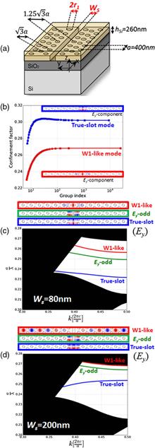
We introduce a family of slot photonic crystal waveguides (SPhCWs) for the hybrid integration of low-index active materials in silicon photonics with energy-confinement factors of ~30% in low-index regions. The proposed approach, which is based on a periodic indentation of the etched slot in the middle of the SPhCW, makes it possible to reconcile a simultaneously narrow and wide slot for exploiting the two modes of even symmetry of a SPhCW. The resulting mode-selection mechanism allows a flexible choice of the modes to be used. Furthermore, the proposed structure offers tremendous flexibility for adjusting the dispersive properties of the slot-confined modes, in particular of their slow-light effects. Flat band slow light in a bandwidth of about 60 nm with a group velocity dispersion factor |β2| below 1 ps2/mm is numerically demonstrated by this approach, corresponding to a normalized delay bandwidth product of around 0.4. These results, obtained from hollow-core periodic waveguides that are directly designed in view of hybrid integration of active materials in mechanically robust structures (not based on free-standing membranes) could pave the way for the realization of on-chip slow-light bio-sensing, active hybrid-silicon optoelectronic devices, or all-optical hybrid-silicon nonlinear functionalities.We introduce a family of slot photonic crystal waveguides (SPhCWs) for the hybrid integration of low-index active materials in silicon photonics with energy-confinement factors of ~ 30 % | β 2 | 1 ps 2 / mm
Photonics Research
- Publication Date: Dec. 22, 2017
- Vol. 6, Issue 1, 54 (2018)


Two-groove narrowband transmission filter integrated into a slab waveguide
Leonid L. Doskolovich, Evgeni A. Bezus, and Dmitry A. Bykov
We propose a simple integrated narrowband filter consisting of two grooves on the surface of a slab waveguide. Spectral filtering is performed in transmission at oblique incidence due to excitation of an eigenmode of the structure localized at a ridge cavity between the grooves. For the considered parameters, zero reflectance and unity transmittance are achieved at resonant conditions. The width and location of the transmittance peak can be controlled by changing the widths of the grooves and of the ridge, respectively. The proposed filter may find application in waveguide-integrated spectrometers.We propose a simple integrated narrowband filter consisting of two grooves on the surface of a slab waveguide. Spectral filtering is performed in transmission at oblique incidence due to excitation of an eigenmode of the structure localized at a ridge cavity between the grooves. For the considered parameters, zero reflectance and unity transmittance are achieved at resonant conditions. The width and location of the transmittance peak can be controlled by changing the widths of the grooves and of the ridge, respectively. The proposed filter may find application in waveguide-integrated spectrometers..
Photonics Research
- Publication Date: Dec. 22, 2017
- Vol. 6, Issue 1, 61 (2018)
Lasers and Laser Optics
Generation of high-energy narrowband 2.05 μm pulses for seeding a Ho:YLF laser
Yanchun Yin, Xiaoming Ren, Yang Wang, Fengjiang Zhuang... and Zenghu Chang|Show fewer author(s)
We experimentally demonstrate efficient generation of high-energy (82 μJ) narrowband 2.05 μm pulses pumped with 1 mJ broadband Ti:sapphire laser pulses, utilizing dual-chirped optical parametric amplification (DC-OPA) in a BBO crystal. The narrowband 2.05 μm pulses will be primarily used for seeding an Ho:YLF laser, which solves the synchronization issue when Ti:sapphire and Ho:YLF lasers are needed for developing midinfrared lasers. The narrowband 2.05 μm pulse from the unique DC-OPA design can seed the Ho:YLF laser much more efficiently than the broadband 2.05 μm pulse from traditional OPA technology.We experimentally demonstrate efficient generation of high-energy (82 μJ) narrowband 2.05 μm pulses pumped with 1 mJ broadband Ti:sapphire laser pulses, utilizing dual-chirped optical parametric amplification (DC-OPA) in a BBO crystal. The narrowband 2.05 μm pulses will be primarily used for seeding an Ho:YLF laser, which solves the synchronization issue when Ti:sapphire and Ho:YLF lasers are needed for developing midinfrared lasers. The narrowband 2.05 μm pulse from the unique DC-OPA design can seed the Ho:YLF laser much more efficiently than the broadband 2.05 μm pulse from traditional OPA technology..
Photonics Research
- Publication Date: Dec. 05, 2017
- Vol. 6, Issue 1, 1 (2018)
Metamaterials
Polarization-independent all-silicon dielectric metasurfaces in the terahertz regime
Huifang Zhang, Xueqian Zhang, Quan Xu, Qiu Wang... and Weili Zhang|Show fewer author(s)
Dielectric metasurfaces have achieved great success in realizing high-efficiency wavefront control in the optical and infrared ranges. Here, we experimentally demonstrate several efficient, polarization-independent, all-silicon dielectric metasurfaces in the terahertz regime. The metasurfaces are composed of cylindrical silicon pillars on a silicon substrate, which can be easily fabricated using etching technology for semiconductors. By locally tailoring the diameter of the pillars, full control over abrupt phase changes can be achieved. To show the controlling ability of the metasurfaces, an anomalous deflector, three Bessel beam generators, and three vortex beam generators are fabricated and characterized. We also show that the proposed metasurfaces can be easily combined to form composite devices with extended functionalities. The proposed controlling method has promising applications in developing low-loss, ultra-compact spatial terahertz modulation devices.Dielectric metasurfaces have achieved great success in realizing high-efficiency wavefront control in the optical and infrared ranges. Here, we experimentally demonstrate several efficient, polarization-independent, all-silicon dielectric metasurfaces in the terahertz regime. The metasurfaces are composed of cylindrical silicon pillars on a silicon substrate, which can be easily fabricated using etching technology for semiconductors. By locally tailoring the diameter of the pillars, full control over abrupt phase changes can be achieved. To show the controlling ability of the metasurfaces, an anomalous deflector, three Bessel beam generators, and three vortex beam generators are fabricated and characterized. We also show that the proposed metasurfaces can be easily combined to form composite devices with extended functionalities. The proposed controlling method has promising applications in developing low-loss, ultra-compact spatial terahertz modulation devices..
Photonics Research
- Publication Date: Dec. 12, 2017
- Vol. 6, Issue 1, 24 (2018)
Microwave Photonics
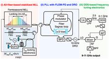
All-fiber-photonics-based ultralow-noise agile frequency synthesizer for X-band radars
Juan Wei, Dohyeon Kwon, Shuangyou Zhang, Shilong Pan, and Jungwon Kim
We propose and demonstrate an agile X-band signal synthesizer with ultralow phase noise based on all-fiber-photonic techniques for radar applications. It shows phase noise of ?145 dBc/Hz (?152 dBc/Hz) at 10 kHz (100 kHz) offset frequency for 10 GHz carrier frequency with integrated RMS timing jitter between 7.6 and 9.1 fs (integration bandwidth: 10 Hz–10 MHz) for frequencies from 9 to 11 GHz. Its frequency switching time is evaluated to be 135 ns with a 135 pHz frequency tuning resolution. In addition, the X-band linear-frequency-modulated signal generated by the proposed synthesizer shows a good pulse compression ratio approximating the theoretical value. In addition to the ultrastable X-band signals, the proposed synthesizer can also provide 0–1 GHz ultralow-jitter clocks for analog-to-digital converters (ADC) and digital-to-analog converters (DAC) in radar systems and ultralow-jitter optical pulse trains for photonic ADC in photonic radar systems. The proposed X-band synthesizer shows great performance in phase stability, switching speed, and modulation capability with robustness and potential low cost, which is enabled by an all-fiber-photonics platform and can be a compelling technology suitable for future X-band radars.We propose and demonstrate an agile X-band signal synthesizer with ultralow phase noise based on all-fiber-photonic techniques for radar applications. It shows phase noise of
Photonics Research
- Publication Date: Dec. 13, 2017
- Vol. 6, Issue 1, 12 (2018)
Silicon Photonics

Single-chip Si optical single-sideband modulator | On the Cover
Byung-Min Yu, Jeong-Min Lee, Christian Mai, Stefan Lischke... and Woo-Young Choi|Show fewer author(s)
We demonstrate an integrated Si optical single-sideband (OSSB) modulator composed of a parallel dual-ring modulator (PDRM) and a quadrature hybrid coupler (QHC). Both the PDRM and the QHC are carefully designed for 30 GHz opearation, and their operations are verified by measurement. The Si OSSB modulator successfully generates a single sideband with larger than 15 dB suppression of the undesired sideband.We demonstrate an integrated Si optical single-sideband (OSSB) modulator composed of a parallel dual-ring modulator (PDRM) and a quadrature hybrid coupler (QHC). Both the PDRM and the QHC are carefully designed for 30 GHz opearation, and their operations are verified by measurement. The Si OSSB modulator successfully generates a single sideband with larger than 15 dB suppression of the undesired sideband..
Photonics Research
- Publication Date: Dec. 06, 2017
- Vol. 6, Issue 1, 6 (2018)
Surface Plasmons
Terahertz spoof surface-plasmon-polariton subwavelength waveguide
Ying Zhang, Yuehong Xu, Chunxiu Tian, Quan Xu... and Weili Zhang|Show fewer author(s)
Surface plasmon polaritons (SPPs) with the features of subwavelength confinement and strong enhancements have sparked enormous interest. However, in the terahertz regime, due to the perfect conductivities of most metals, it is hard to realize the strong confinement of SPPs, even though the propagation loss could be sufficiently low. One main approach to circumvent this problem is to exploit spoof SPPs, which are expected to exhibit useful subwavelength confinement and relative low propagation loss at terahertz frequencies. Here we report the design, fabrication, and characterization of terahertz spoof SPP waveguides based on corrugated metal surfaces. The various waveguide components, including a straight waveguide, an S-bend waveguide, a Y-splitter, and a directional coupler, were experimentally demonstrated using scanning near-field terahertz microscopy. The proposed waveguide indeed enables propagation, bending, splitting, and coupling of terahertz SPPs and thus paves a new way for the development of flexible and compact plasmonic circuits operating at terahertz frequencies.Surface plasmon polaritons (SPPs) with the features of subwavelength confinement and strong enhancements have sparked enormous interest. However, in the terahertz regime, due to the perfect conductivities of most metals, it is hard to realize the strong confinement of SPPs, even though the propagation loss could be sufficiently low. One main approach to circumvent this problem is to exploit spoof SPPs, which are expected to exhibit useful subwavelength confinement and relative low propagation loss at terahertz frequencies. Here we report the design, fabrication, and characterization of terahertz spoof SPP waveguides based on corrugated metal surfaces. The various waveguide components, including a straight waveguide, an S-bend waveguide, a Y-splitter, and a directional coupler, were experimentally demonstrated using scanning near-field terahertz microscopy. The proposed waveguide indeed enables propagation, bending, splitting, and coupling of terahertz SPPs and thus paves a new way for the development of flexible and compact plasmonic circuits operating at terahertz frequencies..
Photonics Research
- Publication Date: Dec. 13, 2017
- Vol. 6, Issue 1, 18 (2018)
Enhanced light emission from AlGaN/GaN multiple quantum wells using the localized surface plasmon effect by aluminum nanoring patterns
Kyung Rock Son, Byeong Ryong Lee, Min Ho Jang, Hyun Chul Park... and Tae Geun Kim|Show fewer author(s)
We investigate the localized surface plasmon (LSP) effect by Al nanorings on the AlGaN/GaN multiple quantum well (MQW) structure emitting at 365 nm. For this experiment, first, the size of Al nanorings is optimized to maximize the energy transfer (or coupling) between the LSP and MQW using the silica nanospheres. Then, the Al nanorings with an outer diameter of 385 nm, which exhibit a strong absorption peak in the near-ultraviolet region, are applied to the top surface of the AlGaN/GaN MQW. The photoluminescence (PL) intensity of the MQW structure with Al nanorings increased by 227% at 365 nm compared to that without Al nanorings. This improvement is mainly attributed to an enhanced radiative recombination rate in the MQWs through the energy-matched LSPs by the temperature-dependent PL and time-resolved PL analyses. The radiative lifetime was about two times shorter than that of the structure without Al nanorings at room temperature. In addition, the measured PL efficiency at room temperature of the structure with Al nanorings was 33%, while that of the structure without Al nanorings was 19%, implying that LSP-QW coupling together with the nanoring array pattern itself played important roles in the enhancement.We investigate the localized surface plasmon (LSP) effect by Al nanorings on the AlGaN/GaN multiple quantum well (MQW) structure emitting at 365 nm. For this experiment, first, the size of Al nanorings is optimized to maximize the energy transfer (or coupling) between the LSP and MQW using the silica nanospheres. Then, the Al nanorings with an outer diameter of 385 nm, which exhibit a strong absorption peak in the near-ultraviolet region, are applied to the top surface of the AlGaN/GaN MQW. The photoluminescence (PL) intensity of the MQW structure with Al nanorings increased by 227% at 365 nm compared to that without Al nanorings. This improvement is mainly attributed to an enhanced radiative recombination rate in the MQWs through the energy-matched LSPs by the temperature-dependent PL and time-resolved PL analyses. The radiative lifetime was about two times shorter than that of the structure without Al nanorings at room temperature. In addition, the measured PL efficiency at room temperature of the structure with Al nanorings was 33%, while that of the structure without Al nanorings was 19%, implying that LSP-QW coupling together with the nanoring array pattern itself played important roles in the enhancement..
Photonics Research
- Publication Date: Dec. 14, 2017
- Vol. 6, Issue 1, 30 (2018)
Deep-subwavelength light transmission in hybrid nanowire-loaded silicon nano-rib waveguides
Yusheng Bian, Qiang Ren, Lei Kang, Taiwei Yue... and Douglas H. Werner|Show fewer author(s)
Hybrid plasmonic waveguides leveraging the coupling between dielectric modes and plasmon polaritons have emerged as a major focus of research attention during the past decade. A feasible way for constructing practical hybrid plasmonic structures is to integrate metallic configurations with silicon-on-insulator waveguiding platforms. Here we report a transformative high-performance silicon-based hybrid plasmonic waveguide that consists of a silicon nano-rib loaded with a metallic nanowire. A deep-subwavelength mode area (λ2/4.5×105 λ2/7×103), in conjunction with a reasonable propagation distance (2.2–60.2 μm), is achievable at a telecommunication wavelength of 1.55 μm. Such a nano-rib-based waveguide outperforms its conventional hybrid and plasmonic waveguiding counterparts, demonstrating tighter optical confinement for similar propagation distances and a significantly enhanced figure of merit. The guiding properties of the fundamental mode are also quite robust against possible fabrication imperfections. Due to the strong confinement capability, our proposed hybrid configuration features ultralow waveguide cross talk and enables submicron bends with moderate attenuation as well. The outstanding optical performance renders such waveguides as promising building blocks for ultracompact passive and active silicon-based integrated photonic components.Hybrid plasmonic waveguides leveraging the coupling between dielectric modes and plasmon polaritons have emerged as a major focus of research attention during the past decade. A feasible way for constructing practical hybrid plasmonic structures is to integrate metallic configurations with silicon-on-insulator waveguiding platforms. Here we report a transformative high-performance silicon-based hybrid plasmonic waveguide that consists of a silicon nano-rib loaded with a metallic nanowire. A deep-subwavelength mode area (λ 2 / 4.5 × 10 5 λ 2 / 7 × 10 3
Photonics Research
- Publication Date: Dec. 15, 2017
- Vol. 6, Issue 1, 37 (2018)
On-chip polarization splitter based on a multimode plasmonic waveguide
Fengyuan Gan, Chengwei Sun, Hongyun Li, Qihuang Gong, and Jianjun Chen
The miniaturization of polarization beam splitters (PBSs) is vital for ultradense chip-scale photonic integrated circuits. However, the small PBSs based on complex hybrid plasmonic structures exhibit large fabrication difficulties or high insertion losses. Here, by designing a bending multimode plasmonic waveguide, an ultrabroadband on-chip plasmonic PBS with low insertion losses is numerically and experimentally realized. The multimode plasmonic waveguide, consisting of a metal strip with a V-shaped groove on the metal surface, supports the symmetric and antisymmetric surface plasmon polariton (SPP) waveguide modes in nature. Due to the different field confinements of the two SPP waveguide modes, which result in different bending losses, the two incident SPP waveguide modes of orthogonal polarization states are efficiently split in the bending multimode plasmonic waveguide. The numerical simulations show that the operation bandwidth of the proposed PBS is as large as 430 nm because there is no resonance or interference effect in the splitting process. Compared with the complex hybrid plasmonic structure, the simple bending multimode plasmonic waveguide is much easier to fabricate. In the experiment, a broadband (Δλ≈120 nm) and low-insertion-loss (<3 dB with a minimum insertion loss of 0.7 dB) PBS is demonstrated by using the strongly confined waveguide modes as the incident sources in the bending multimode plasmonic waveguide.The miniaturization of polarization beam splitters (PBSs) is vital for ultradense chip-scale photonic integrated circuits. However, the small PBSs based on complex hybrid plasmonic structures exhibit large fabrication difficulties or high insertion losses. Here, by designing a bending multimode plasmonic waveguide, an ultrabroadband on-chip plasmonic PBS with low insertion losses is numerically and experimentally realized. The multimode plasmonic waveguide, consisting of a metal strip with a V-shaped groove on the metal surface, supports the symmetric and antisymmetric surface plasmon polariton (SPP) waveguide modes in nature. Due to the different field confinements of the two SPP waveguide modes, which result in different bending losses, the two incident SPP waveguide modes of orthogonal polarization states are efficiently split in the bending multimode plasmonic waveguide. The numerical simulations show that the operation bandwidth of the proposed PBS is as large as 430 nm because there is no resonance or interference effect in the splitting process. Compared with the complex hybrid plasmonic structure, the simple bending multimode plasmonic waveguide is much easier to fabricate. In the experiment, a broadband (Δ λ ≈ 120 nm < 3 dB
Photonics Research
- Publication Date: Dec. 22, 2017
- Vol. 6, Issue 1, 47 (2018)
Errata

High-efficiency normal-incidence vertical p-i-n photodetectors on a germanium-on-insulator platform: publisher’s note
Yiding Lin, Kwang Hong Lee, Shuyu Bao, Xin Guo... and Chuan Seng Tan|Show fewer author(s)
This publisher’s note reports corrections to Eq. (1) in [Photon. Res.5, 702 (2017)PRHEIZ2327-912510.1364/PRJ.5.000702].This publisher’s note reports corrections to Eq. (1) in [Photon. Res.5 , 702 (2017 )PRHEIZ 2327-9125 10.1364/PRJ.5.000702
Photonics Research
- Publication Date: Dec. 15, 2017
- Vol. 6, Issue 1, 46 (2018)


© Copyright 2018-2021 | Chinese Laser Press. All Rights Reserved 沪ICP备15018463号-20