Contents


2018
Volume: 6 Issue 2
14 Article(s)
Export citation format
OPTICAL MICROCAVITIES
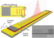
Terahertz emission from localized modes in one-dimensional disordered systems [Invited]
Yongquan Zeng, Guozhen Liang, Bo Qiang, Bo Meng... and Qi Jie Wang|Show fewer author(s)
We demonstrate terahertz (THz) frequency laser emission around 3.2 THz from localized modes in one-dimensional disordered grating systems. The disordered structures are patterned on top of the double-metal waveguide of a THz quantum cascade laser. Multiple emission peaks are observed within a frequency range corresponding to the bandgap of a periodic counterpart with no disorder, indicating the presence of mode localization aided by Bragg scattering. Simulations and experimental measurements provide strong evidence for the spatial localization of the THz laser modes.We demonstrate terahertz (THz) frequency laser emission around 3.2 THz from localized modes in one-dimensional disordered grating systems. The disordered structures are patterned on top of the double-metal waveguide of a THz quantum cascade laser. Multiple emission peaks are observed within a frequency range corresponding to the bandgap of a periodic counterpart with no disorder, indicating the presence of mode localization aided by Bragg scattering. Simulations and experimental measurements provide strong evidence for the spatial localization of the THz laser modes..
Photonics Research
- Publication Date: Jan. 25, 2018
- Vol. 6, Issue 2, 117 (2018)


Optical microcavities: new understandings and developments: publisher’s note
Li Ge, Liang Feng, and Harald G. L. Schwefel
This publisher’s note reports correcting Ref. [12] and adding a reference in [Photon. Res.5, OM1 (2017)2327912510.1364/PRJ.5.000OM1].This publisher’s note reports correcting Ref. [12] and adding a reference in [Photon. Res.5 , OM1 (2017 )23279125 10.1364/PRJ.5.000OM1
Photonics Research
- Publication Date: Jan. 24, 2018
- Vol. 6, Issue 2, 89 (2018)
Research Articles
Fiber Devices
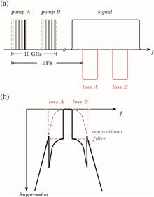
Sharp tunable and additional noise-free optical filter based on Brillouin losses
Cheng Feng, Stefan Preussler, and Thomas Schneider
In this paper, we propose an additional noise-free, independent center frequency and bandwidth tunable optical filter based on stimulated Brillouin scattering (SBS) losses. By suppressing the out-of-band signal with two broadshow moreIn this paper, we propose an additional noise-free, independent center frequency and bandwidth tunable optical filter based on stimulated Brillouin scattering (SBS) losses. By suppressing the out-of-band signal with two broadened symmetric SBS losses, tunable pass bandwidths from 500 MHz to 9.5 GHz and the independent center frequency tunability are demonstrated. Considering the limited SBS interaction in the center frequency range, a flat-top response with minimum 0.3 dB ripple is achieved. Assisted by the extra suppression from polarization pulling, a maximum selectivity of 20 dB and an ultrahigh 250 dB / GHz
Photonics Research
- Publication Date: Jan. 25, 2018
- Vol. 6, Issue 2, 132 (2018)
Lasers and Laser Optics
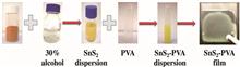
Passively mode-locked Er-doped fiber laser based on SnS2 nanosheets as a saturable absorber
Kangdi Niu, Ruyi Sun, Qingyun Chen, Baoyuan Man, and Huanian Zhang
In this paper, tin disulfide (SnS2), a two-dimensional (2D) n-type direct bandgap layered metal dichalcogenide with a gap value of 2.24 eV, was employed as a saturable absorber. Its appearance and nonlinear saturable absorption characteristics were also investigated experimentally. SnS2-PVA (polyvinyl alcohol) film was successfully prepared and employed as a mode-locker for achieving a mode-locked Er-doped fiber laser with a pulse width of 623 fs at a pulse repetition rate of 29.33 MHz. The results prove that SnS2 nanosheets will have wide potential ultrafast photonic applications due to their suitable bandgap value and excellent nonlinear saturable absorption characteristics.In this paper, tin disulfide (SnS 2 SnS 2 - PVA SnS 2
Photonics Research
- Publication Date: Jan. 24, 2018
- Vol. 6, Issue 2, 72 (2018)

30 W monolithic 2–3 μm supercontinuum laser
Ke Yin, Bin Zhang, Linyong Yang, and Jing Hou
A high-power all-fiber supercontinuum (SC) laser source based on germania-core fiber (GCF) was presented. The lesser absorption loss of GCF than silica fiber beyond 2.0 μm makes GCF more suitable for extending the SC spectrum to the long wavelength side. In this work, the GCF-based SC laser had a maximum power of 30.1 W, together with a 10 dB spectral bandwidth of >1000 nm spanning from 1.95 to 3.0 μm. To the best of our knowledge, this is the highest output power level ever reported for a GCF-based SC laser as well as a 2–3 μm SC laser.A high-power all-fiber supercontinuum (SC) laser source based on germania-core fiber (GCF) was presented. The lesser absorption loss of GCF than silica fiber beyond 2.0 μm makes GCF more suitable for extending the SC spectrum to the long wavelength side. In this work, the GCF-based SC laser had a maximum power of 30.1 W, together with a 10 dB spectral bandwidth of > 1000 nm
Photonics Research
- Publication Date: Jan. 25, 2018
- Vol. 6, Issue 2, 123 (2018)
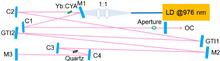
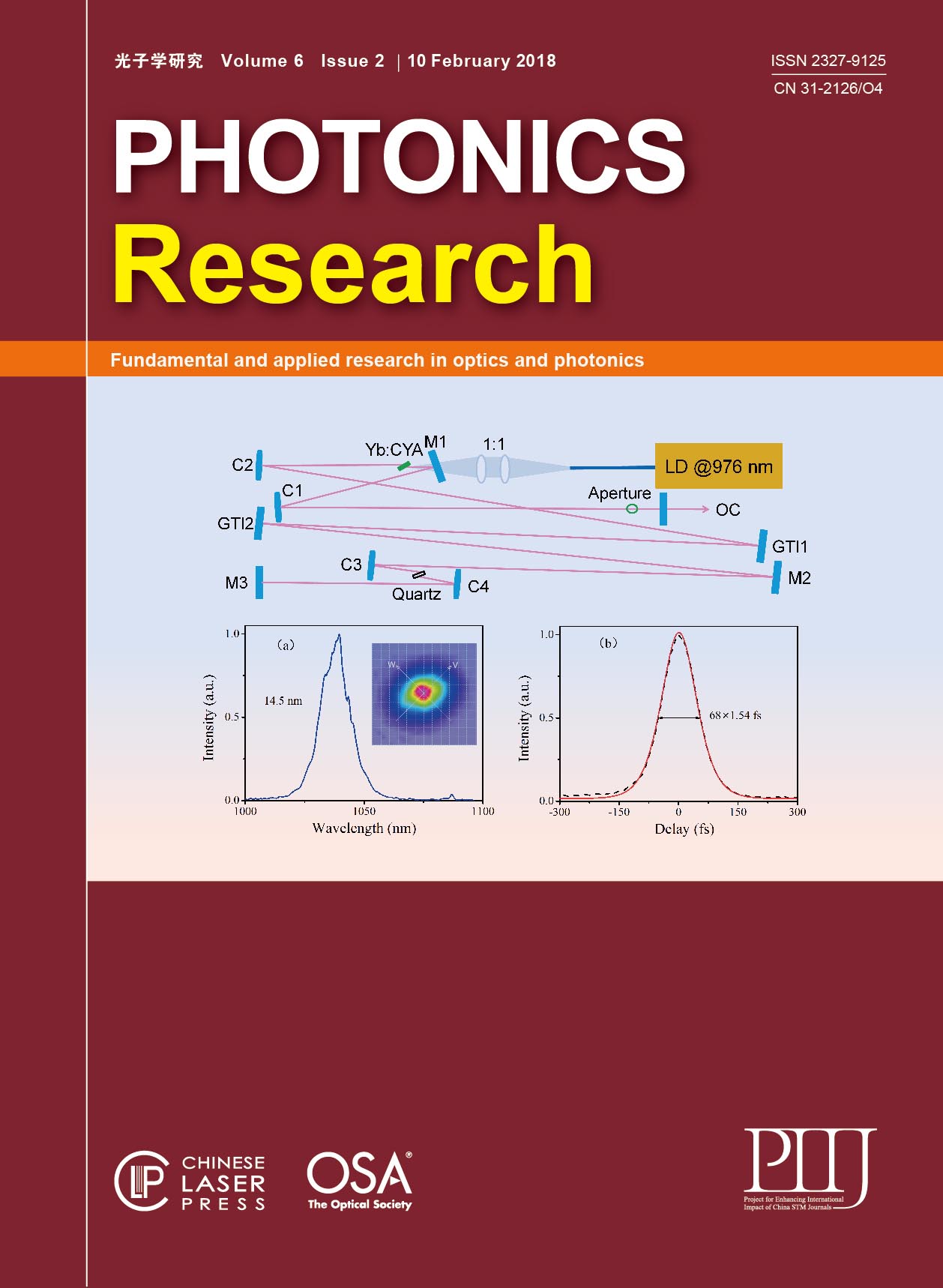
Diode-pumped power scalable Kerr-lens mode-locked Yb:CYA laser | On the Cover
Wenlong Tian, Yingnan Peng, Ziyue Zhang, Zijiao Yu... and Zhiyi Wei|Show fewer author(s)
Stable 68 fs pulses with the average power of 1.5 W is directly generated from a multimode diode-pumped Kerr-lens mode-locked Yb:CYA laser by separating the gain medium and Kerr medium. The repetition rate is about 50 MHz, resulting in a single pulse energy of 30 nJ and a peak power of 0.44 MW. To the best of our knowledge, this is the highest single pulse energy ever produced from a mode-locked Yb:CYA oscillator. Our experimental results show that Yb:CYA crystal is an excellent candidate for multiwatt, sub-100 fs pulse generation in diode-pumped all-solid-state lasers. It is believed that the output power can be scalable to multi-W while the pulse duration is maintained with this simple method.Stable 68 fs pulses with the average power of 1.5 W is directly generated from a multimode diode-pumped Kerr-lens mode-locked Yb:CYA laser by separating the gain medium and Kerr medium. The repetition rate is about 50 MHz, resulting in a single pulse energy of 30 nJ and a peak power of 0.44 MW. To the best of our knowledge, this is the highest single pulse energy ever produced from a mode-locked Yb:CYA oscillator. Our experimental results show that Yb:CYA crystal is an excellent candidate for multiwatt, sub-100 fs pulse generation in diode-pumped all-solid-state lasers. It is believed that the output power can be scalable to multi-W while the pulse duration is maintained with this simple method..
Photonics Research
- Publication Date: Jan. 25, 2018
- Vol. 6, Issue 2, 127 (2018)
Light-emitting Diodes
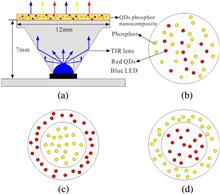
Enhanced optical and thermal performance of white light-emitting diodes with horizontally layered quantum dots phosphor nanocomposites
Shudong Yu, Yong Tang, Zongtao Li, Kaihang Chen... and Binhai Yu|Show fewer author(s)
Due to their good color rendering ability, white light-emitting diodes (WLEDs) with conventional phosphor and quantum dots (QDs) are gaining increasing attention. However, their optical and thermal performances are still limishow moreDue to their good color rendering ability, white light-emitting diodes (WLEDs) with conventional phosphor and quantum dots (QDs) are gaining increasing attention. However, their optical and thermal performances are still limited especially for the ones with QDs-phosphor mixed nanocomposites. In this work, we propose a novel packaging scheme with horizontally layered QDs-phosphor nanocomposites to obtain an enhanced optical and thermal performance for WLEDs. Three different WLEDs, including QDs-phosphor mixed type, QDs-outside type, and QDs-inside type, were fabricated and compared. With 30 wt. % phosphor and 0.15 wt. % QDs nanocomposite, the QDs-outside type WLED shows a 21.8% increase of luminous efficiency, better color rendering ability, and a 27.0% decrease of the maximum nanocomposite temperature at 400 mA, compared with the mixed-type WLED. The reduced re-absorption between phosphor and QDs is responsible for the performance enhancement when they are separated. However, such reduced absorption can be traded off by the improper layered configuration, which is demonstrated by the worst performance of the QDs-inside type. Further, we demonstrate that the higher energy transfer efficiency between excitation light and nanocomposite in the QDs-outside type WLED is the key reason for its enhanced optical and thermal performance..
Photonics Research
- Publication Date: Jan. 24, 2018
- Vol. 6, Issue 2, 90 (2018)
Optical Trapping and Manipulation

All-optical manipulation of micrometer-sized metallic particles
Yuquan Zhang, Xiujie Dou, Yanmeng Dai, Xianyou Wang... and Xiaocong Yuan|Show fewer author(s)
Optical traps use focused laser beams to generate forces on targeted objects ranging in size from nanometers to micrometers. However, for their high coefficients of scattering and absorption, micrometer-sized metallic particles were deemed non-trappable in three dimensions using a single beam. This barrier is now removed. We demonstrate, both in theory and experiment, three-dimensional (3D) dynamic all-optical manipulations of micrometer-sized gold particles under high focusing conditions. The force of gravity is found to balance the positive axial optical force exerted on particles in an inverted optical tweezers system to form two trapping positions along the vertical direction. Both theoretical and experimental results confirm that stable 3D manipulations are achievable for these particles regardless of beam polarization and wavelength. The present work opens up new opportunities for a variety of in-depth research requiring metallic particles.Optical traps use focused laser beams to generate forces on targeted objects ranging in size from nanometers to micrometers. However, for their high coefficients of scattering and absorption, micrometer-sized metallic particles were deemed non-trappable in three dimensions using a single beam. This barrier is now removed. We demonstrate, both in theory and experiment, three-dimensional (3D) dynamic all-optical manipulations of micrometer-sized gold particles under high focusing conditions. The force of gravity is found to balance the positive axial optical force exerted on particles in an inverted optical tweezers system to form two trapping positions along the vertical direction. Both theoretical and experimental results confirm that stable 3D manipulations are achievable for these particles regardless of beam polarization and wavelength. The present work opens up new opportunities for a variety of in-depth research requiring metallic particles..
Photonics Research
- Publication Date: Jan. 16, 2018
- Vol. 6, Issue 2, 66 (2018)
Plasmonics
Bionic SERS chip with super-hydrophobic and plasmonic micro/nano dual structure
Fengyou Yang, Haoran Zhang, Huimin Feng, Jianjie Dong... and Qian Liu|Show fewer author(s)
Natural surface-enhanced Raman spectroscopy (SERS) chips based on plants or insects have gained increased attention due to their facile characteristics and low costs. However, such chips remain a major challenge for practicalshow moreNatural surface-enhanced Raman spectroscopy (SERS) chips based on plants or insects have gained increased attention due to their facile characteristics and low costs. However, such chips remain a major challenge for practical application because of poor reproducibility and stability as well as unavoidable damage to the surface structure during coating metal and uncontrolled dehydration. By using a simple wrinkling method, we develop a new route to fabricate a low-cost bionic SERS chip for practical detection. Inspired by the taro leaf, we fabricate a SERS chip with a super-hydrophobic and plasmonic micro/nano dual structure, and its structure parameters can be optimized. Compared with the natural taro-leaf SERS chip, our artificial chip exhibits Raman signals with an order of magnitude higher sensitivity (~ 10 9 M ~ 10 7
Photonics Research
- Publication Date: Jan. 24, 2018
- Vol. 6, Issue 2, 77 (2018)
Single nanoparticle trapping based on on-chip nanoslotted nanobeam cavities
Daquan Yang, Fei Gao, Qi-Tao Cao, Chuan Wang... and Yun-Feng Xiao|Show fewer author(s)
Optical trapping techniques are of great interest since they have the advantage of enabling the direct handling of nanoparticles. Among various optical trapping systems, photonic crystal nanobeam cavities have attracted greatshow moreOptical trapping techniques are of great interest since they have the advantage of enabling the direct handling of nanoparticles. Among various optical trapping systems, photonic crystal nanobeam cavities have attracted great attention for integrated on-chip trapping and manipulation. However, optical trapping with high efficiency and low input power is still a big challenge in nanobeam cavities because most of the light energy is confined within the solid dielectric region. To this end, by incorporating a nanoslotted structure into an ultracompact one-dimensional photonic crystal nanobeam cavity structure, we design a promising on-chip device with ultralarge trapping potential depth to enhance the optical trapping characteristic of the cavity. In this work, we first provide a systematic analysis of the optical trapping force for an airborne polystyrene (PS) nanoparticle trapped in a cavity model. Then, to validate the theoretical analysis, the numerical simulation proof is demonstrated in detail by using the three-dimensional finite element method. For trapping a PS nanoparticle of 10 nm radius within the air-slot, a maximum trapping force as high as 8.28 nN/mW and a depth of trapping potential as large as 1.15 × 10 5 k B T m W 1 k B T 167.17 pN · nm 1 · mW 1 x
Photonics Research
- Publication Date: Jan. 24, 2018
- Vol. 6, Issue 2, 99 (2018)
Silicon Photonics
Silicon intensity Mach–Zehnder modulator for single lane 100 Gb/s applications
Miaofeng Li, Lei Wang, Xiang Li, Xi Xiao, and Shaohua Yu
In this paper, a substrate removing technique in a silicon Mach–Zehnder modulator (MZM) is proposed and demonstrated to improve modulation bandwidth. Based on the novel and optimized traveling wave electrodes, the electrode transmission loss is reduced, and the electro-optical group index and 50 Ω impedance matching are improved, simultaneously. A 2 mm long substrate removed silicon MZM with the measured and extrapolated 3 dB electro-optical bandwidth of >50 GHz and 60 GHz at the 8 V bias voltage is designed and fabricated. Open optical eye diagrams of up to 90 GBaud/s NRZ and 56 GBaud/s four-level pulse amplitude modulation (PAM-4) are experimentally obtained without additional optical or digital compensations. Based on this silicon MZM, the performance in a short-reach transmission system is further investigated. Single-lane 112 Gb/s and 128 Gb/s transmissions over different distances of 1 km, 2 km, and 10 km are experimentally achieved based on this high-speed silicon MZM.In this paper, a substrate removing technique in a silicon Mach–Zehnder modulator (MZM) is proposed and demonstrated to improve modulation bandwidth. Based on the novel and optimized traveling wave electrodes, the electrode transmission loss is reduced, and the electro-optical group index and 50 Ω > 50 GHz 8 V 90 GBaud / s 56 GBaud / s 112 Gb / s 128 Gb / s
Photonics Research
- Publication Date: Jan. 24, 2018
- Vol. 6, Issue 2, 109 (2018)
Ultrafast Optics
Effect of anti-crossings with cladding resonances on ultrafast nonlinear dynamics in gas-filled photonic crystal fibers
F. Tani, F. Köttig, D. Novoa, R. Keding, and P. St.J. Russell
Spectral anti-crossings between the fundamental guided mode and core-wall resonances alter the dispersion in hollow-core anti-resonant-reflection photonic crystal fibers. Here we study the effect of this dispersion change on the nonlinear propagation and dynamics of ultrashort pulses. We find that it causes emission of narrow spectral peaks through a combination of four-wave mixing and dispersive wave emission. We further investigate the influence of the anti-crossings on nonlinear pulse propagation and show that their impact can be minimized by adjusting the core-wall thickness in such a way that the anti-crossings lie spectrally distant from the pump wavelength.Spectral anti-crossings between the fundamental guided mode and core-wall resonances alter the dispersion in hollow-core anti-resonant-reflection photonic crystal fibers. Here we study the effect of this dispersion change on the nonlinear propagation and dynamics of ultrashort pulses. We find that it causes emission of narrow spectral peaks through a combination of four-wave mixing and dispersive wave emission. We further investigate the influence of the anti-crossings on nonlinear pulse propagation and show that their impact can be minimized by adjusting the core-wall thickness in such a way that the anti-crossings lie spectrally distant from the pump wavelength..
Photonics Research
- Publication Date: Jan. 24, 2018
- Vol. 6, Issue 2, 84 (2018)
Optical forces of focused femtosecond laser pulses on nonlinear optical Rayleigh particles
Liping Gong, Bing Gu, Guanghao Rui, Yiping Cui... and Qiwen Zhan|Show fewer author(s)
The principle of optical trapping is conventionally based on the interaction of optical fields with linear-induced polarizations. However, the optical force originating from the nonlinear polarization becomes significant when nonlinear optical nanoparticles are trapped by femtosecond laser pulses. Herein we develop the time-averaged optical forces on a nonlinear optical nanoparticle using high-repetition-rate femtosecond laser pulses, based on the linear and nonlinear polarization effects. We investigate the dependence of the optical forces on the magnitudes and signs of the refractive nonlinearities. It is found that the self-focusing effect enhances the trapping ability, whereas the self-defocusing effect leads to the splitting of the potential well at the focal plane and destabilizes the optical trap. Our results show good agreement with the reported experimental observations and provide theoretical support for capturing nonlinear optical particles.The principle of optical trapping is conventionally based on the interaction of optical fields with linear-induced polarizations. However, the optical force originating from the nonlinear polarization becomes significant when nonlinear optical nanoparticles are trapped by femtosecond laser pulses. Herein we develop the time-averaged optical forces on a nonlinear optical nanoparticle using high-repetition-rate femtosecond laser pulses, based on the linear and nonlinear polarization effects. We investigate the dependence of the optical forces on the magnitudes and signs of the refractive nonlinearities. It is found that the self-focusing effect enhances the trapping ability, whereas the self-defocusing effect leads to the splitting of the potential well at the focal plane and destabilizes the optical trap. Our results show good agreement with the reported experimental observations and provide theoretical support for capturing nonlinear optical particles..
Photonics Research
- Publication Date: Jan. 26, 2018
- Vol. 6, Issue 2, 138 (2018)
Valence state manipulation of Sm3+ ions via a phase-shaped femtosecond laser field
Ye Zheng, Yunhua Yao, Lianzhong Deng, Wenjing Cheng... and Shian Zhang|Show fewer author(s)
The ability to manipulate the valence state conversion of rare-earth ions is crucial for their applications in color displays, optoelectronic devices, laser sources, and optical memory. The conventional femtosecond laser pulsshow moreThe ability to manipulate the valence state conversion of rare-earth ions is crucial for their applications in color displays, optoelectronic devices, laser sources, and optical memory. The conventional femtosecond laser pulse has been shown to be a well-established tool for realizing the valence state conversion of rare-earth ions, although the valence state conversion efficiency is relatively low. Here, we first propose a femtosecond laser pulse shaping technique for improving the valence state conversion efficiency of rare-earth ions. Our experimental results demonstrate that the photoreduction efficiency from Sm 3 + Sm 2 + Sm 3 + π 2 + 1 Sm 3 + Sm 2 + π
Photonics Research
- Publication Date: Jan. 30, 2018
- Vol. 6, Issue 2, 144 (2018)
About the Cover
On the top: Schematic diagram of the high-power Kerr-lens mode-locked Yb:CYA laser by introducing an extra Kerr-medium to separate the gain material and Kerr material. On the bottom: (a) Continuous wave and mode-locked spectra with an inset of the beam profile at the maximum average power of 1.5 W. (b) Measured (black dash) and fitted (red) intensity autocorrelation trace.

© Copyright 2018-2021 | Chinese Laser Press. All Rights Reserved 沪ICP备15018463号-20