Abstract
Hybrid plasmonic waveguides leveraging the coupling between dielectric modes and plasmon polaritons have emerged as a major focus of research attention during the past decade. A feasible way for constructing practical hybrid plasmonic structures is to integrate metallic configurations with silicon-on-insulator waveguiding platforms. Here we report a transformative high-performance silicon-based hybrid plasmonic waveguide that consists of a silicon nano-rib loaded with a metallic nanowire. A deep-subwavelength mode area (), in conjunction with a reasonable propagation distance (2.2–60.2 μm), is achievable at a telecommunication wavelength of 1.55 μm. Such a nano-rib-based waveguide outperforms its conventional hybrid and plasmonic waveguiding counterparts, demonstrating tighter optical confinement for similar propagation distances and a significantly enhanced figure of merit. The guiding properties of the fundamental mode are also quite robust against possible fabrication imperfections. Due to the strong confinement capability, our proposed hybrid configuration features ultralow waveguide cross talk and enables submicron bends with moderate attenuation as well. The outstanding optical performance renders such waveguides as promising building blocks for ultracompact passive and active silicon-based integrated photonic components.1. INTRODUCTION
The field of nanophotonics has witnessed a number of significant breakthroughs in both the fundamental and applied aspects during the past few decades due mainly to the remarkable advancements in micro/nanofabrication techniques [1]. The ever-increasing demand for small-footprint and high-performance nanophotonic devices represents a top priority in the development of next-generation optical communication systems and data centers [2,3]. As a rapidly emerging branch of nanophotonics, plasmonics, which exploit the unique optical properties of metallic nanostructures, have been widely employed for light manipulation at the subwavelength scale due to its unprecedented potential to break the fundamental diffraction limit [4,5]. Among the wide variety of guided plasmonic configurations being studied, hybrid plasmonic waveguides (HPWs), which integrate plasmonic configurations and high-index dielectric structures, have recently received particular attention [6–8]. Because of the remarkable ability to provide an improved balance between confinement and loss over their conventional plasmonic counterparts, HPWs enable simultaneously subwavelength field confinement and long-range propagation from optical frequencies to the near-infrared. Owing to their unprecedented ability for highly efficient light transmission, hybrid plasmonics have been regarded as one of the key enabling technologies for the next-generation of integrated optical components and circuits [9]. Besides their outstanding guiding properties, HPWs also provide excellent compatibility with semiconductor materials, thereby potentially offering a promising platform that allows seamless integration with silicon photonics [10,11].
In addition to the extensive efforts that have been devoted to various high-performance integrated nanophotonic devices and the related applications enabled by HPWs [12–18], tremendous emphasis has been placed in recent years on expanding the family of modified hybrid configurations with interesting waveguiding properties [9,10,19–28]. These hybrid waveguides greatly extend the original hybridization concept and result in further improvement of optical performance. One significant advancement in this field involves the long-range HPWs constructed by symmetric or quasi-symmetric hybridized configurations [19,24,26,27]. Owing to improved modal coupling, the propagation distance of a conventional HPW can be dramatically extended while maintaining a subwavelength mode area. Another promising direction is to further push the size of the guided mode down to a scale far below the diffraction limit, while maintaining a reasonable propagation distance. This goal has been accomplished through introducing strongly confined plasmonic modes in different metallic nanostructures, such as metal wedges [28,29], ridges [25], grooves [30], slots [22,23], and so on. Despite the fact that a variety of these modified structures are capable of improving a certain aspect of the guiding performance, most of them are still subject to the trade-off between modal attenuation and field localization. Moreover, the practical implementation of these structures remains a major challenge due to the additional fabrication complexities introduced in the design. Therefore, an improved solution that can not only provide an efficient pathway toward outstanding optical performance but also take full consideration of the practical issues becomes a formidable goal that has been highly sought after.
A feasible strategy for mapping out a practical route toward the implementation of the hybrid concept is to construct HPWs on a silicon-on-insulator (SOI) substrate [10,12,20,22]. Silicon photonics, which hold great promise for low-cost large-scale photonic integration [31,32], can be an ideal platform to construct a variety of passive and active hybrid plasmonic devices. On the other hand, as one of the most important plasmonic guiding elements, metallic nanowires are widely utilized to build high-quality functional integrated components as well [33,34]. Therefore, combing the silicon waveguide platform with metal nanowires (i.e., “the best of both worlds”) could potentially lead to a new class of hybridized structures that not only feature outstanding guiding performance but also offer a feasible route toward realistic devices. In this paper, we show that such a goal can be realized simply by integrating a metallic nanowire with a silicon nano-rib substrate. Owing to the efficient hybridization of the nanowire plasmon polariton and the silicon nano-rib waveguide mode, the hybrid nanowire-loaded nano-rib waveguide features an extremely small mode size (down to the deep-subwavelength scale) while maintaining a reasonable propagation distance at telecommunication wavelengths. In the following, comprehensive studies of the guided mode properties will be discussed in detail and systematic comparisons between our proposed structure and the existing state-of-the-art subwavelength plasmonic waveguides will be carried out to confirm its superior optical performance. In addition, investigations concerning practical issues, such as fabrication tolerance, mode excitation, waveguide bending, and cross talk, will be conducted. Alternative configurations to the waveguide in our case study will be suggested as well, which are expected to pave the way for future design innovations.
Sign up for Photonics Research TOC. Get the latest issue of Photonics Research delivered right to you!Sign up now
2. WAVEGUIDE GEOMETRY AND MODAL PROPERTIES
The geometry of our proposed hybrid nano-rib structure is shown schematically in Fig. 1. The structure consists of a metallic nanowire located above a silicon nano-rib waveguide, with a thin silica layer coating on the silicon slab. Owing to the unique waveguide configuration, a hybrid, nonuniform, low-index gap is formed between the upper metal nanowire and the lower silicon substrate, which facilitates the coupling between the nanowire plasmon and the silicon nano-rib photonic modes. Such an enhanced interaction between the optical field and complex nanostructures results in a strong localization of the hybrid mode within and near the gap region, which is the key to realizing a deep-subwavelength mode size and extremely tight field confinement.
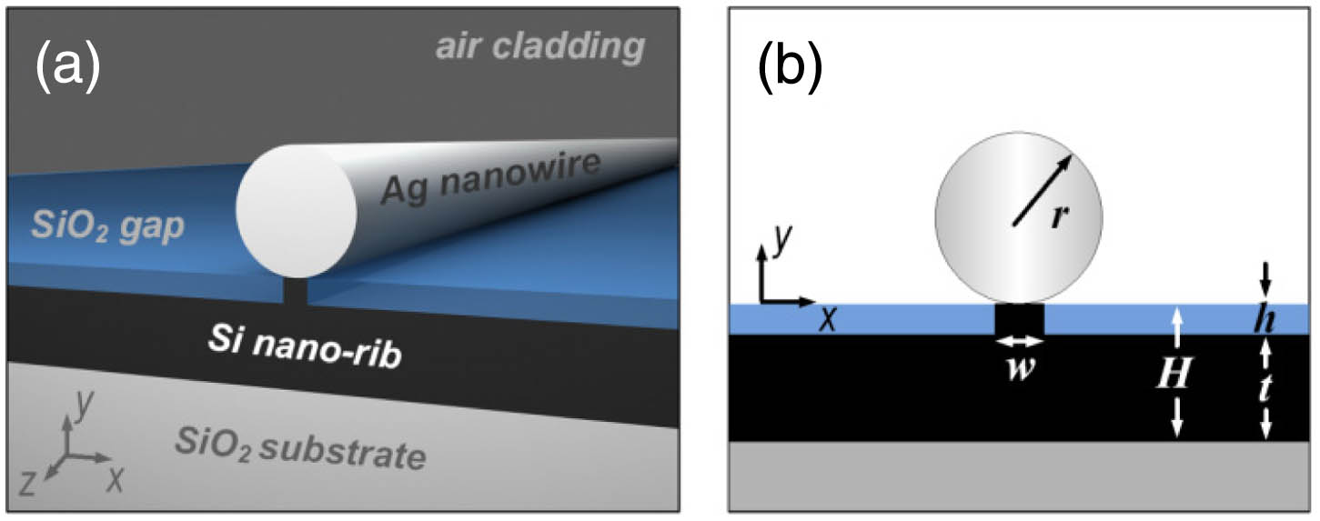
Figure 1.Hybrid nanowire-loaded silicon nano-rib waveguide. (a) Schematic of the 3D geometry. (b) Cross section of the configuration within the plane. The hybrid waveguide comprises a silver nanowire (with a radius of ) located above a silicon nano-rib structure on a silica substrate. An additional silica buffer layer (with a height of ) is sandwiched between the nanowire and the silicon slab, which also determines the gap size (i.e., ). The height of the silicon waveguide is , and the rib width is . The nanowire is positioned at the center (along the axis) with respect to the silicon nano-rib.
The modal properties of the hybrid nanowire-loaded nano-rib waveguides are characterized by a complex wave vector, whose parallel component defines the propagating constant with . Here, and are the phase and attenuation constants, respectively. The real part of the modal effective index is obtained as , where is the vacuum wavevector. The propagation length is calculated using , whereas the effective mode area is defined as the ratio of the total mode energy and the maximum electromagnetic energy density [6]:
In order to accurately account for the energy in the metallic region, the electromagnetic energy density is defined as [6,35] In Eq. (2), and are the electric and magnetic fields, respectively, and and are the electric permittivity and the vacuum magnetic permeability, respectively.
The normalized effective mode area is defined as the ratio of to (i.e., ), where is the diffraction-limited mode area in free space. The figure of merit (FoM) is obtained by calculating the ratio of the propagation length () to the diameter of the effective mode area [] [36]. Finally, the confinement factor is defined as the ratio of the power inside a specific region (e.g., hybrid gap, silicon nano-rib, etc.) to the total power of the waveguide. In the following, the above properties are investigated numerically by solving the Helmholtz equation using the eigenmode solver of COMSOL Multiphysics, a finite-element-method-based software package. A scattering boundary condition is adopted to mimic the open boundary. Convergence tests were performed on the numerical solutions, indicating that the boundary conditions and meshing employed in the models were sound. In the simulations, the refractive indices of silica, silicon, air, and silver at an operating wavelength of 1550 nm are taken as 1.444, 3.476, 1, and [6], respectively. Without loss of generality, a circular-shaped silver nanowire and a rectangular-shaped silicon nano-rib were chosen as a proof-of-concept demonstration. However, our studies have shown that the waveguide concept presented here can also be applied to many other configurations with similar nanostructures, such as silicon nanowedges and nanowires as well as metallic films and stripes.
Here, by investigating the field profile of the fundamental hybrid plasmonic mode sustained in a typical hybrid nanowire-loaded nano-rib waveguide, we are able to further reveal the strong optical confinement present in the configuration. Figure 2 shows the 2D and 1D normalized electric field distributions of the fundamental plasmonic mode supported by a typical hybrid nano-rib waveguide. Owing to the efficient coupling between the metallic nanowire and silicon nano-rib waveguide modes, significant local field enhancements along both the horizontal and vertical directions can be observed inside the nanoscale, hybrid gap region. This is quite beneficial for achieving ultratight field confinement and squeezing the optical mode into an ultrasmall space. The air and silica gaps on each side of the silicon nano-rib not only enable the storage of a reasonable portion of the mode power, but also play a key role in maintaining a relatively low transmission loss in the waveguide.

Figure 2.Normalized electric field distributions of the fundamental hybrid plasmonic mode supported by a typical hybrid nanowire-loaded nano-rib waveguide. The geometric parameters of the waveguide are , , , and . (a) 2D electric field profile in the plane. 1D electric field plots along the (b) and (c) directions, respectively. The 1D field profiles are evaluated at the bottom corner of the silver nanowire.
Our studies indicate that the hybridization of the nanowire plasmon and silicon photonic modes in the hybrid waveguide can be readily regulated by way of tuning its key structural parameters. Here we first look into the effect of nanowire size and thickness of the silicon slab on the waveguiding properties. In order to ensure moderate propagation loss, deep-subwavelength mode size and reasonable confinement inside the gap and silicon waveguide region, and are fixed at 10 and 5 nm, respectively, whereas varies between 10 and 80 nm for different silicon slab thicknesses (20, 40, and 60 nm). As illustrated in Fig. 3, due to the gradually enhanced field confinement, increased modal effective index, reduced mode size, and decreased propagation distance are all observable for waveguides with various slab thicknesses when the nanowire becomes smaller. Similar optical performance, with stronger optical confinement and increased modal attenuation, can be achieved as well through increasing the thickness of the silicon slab. Within the considered geometric parameter range, the mode area of the hybrid nano-rib waveguide can be maintained at the ultradeep-subwavelength scale (). This is more than 1–3 orders of magnitude smaller than that of the conventional HPW () [6] while also being significantly smaller than the recently demonstrated high-performance nanowire-over-substrate configuration [37]. Reasonable propagation distances ( to 60.2 μm) and large FoMs can be achieved simultaneously with such an ultrasmall mode size. In addition, our calculations reveal that the ratios of the modal power residing in the hybrid gap region and the silicon nano-rib structure are also higher than those achieved by the conventional HPW [6] and nanowire-over-substrate configurations [37], which further confirm the outstanding confinement capability of our proposed hybrid waveguide.
Figure 3.Dependence of modal properties on the radius of the silver nanowire for a silicon slab with different thicknesses (, ): (a) modal effective index (); (b) propagation length (), inset showing schematically the considered hybrid gap region in the study; (c) normalized mode area (); (d) confinement factor in the hybrid gap (); (e) confinement factor inside the silicon region (); (f) FoM. The dashed black line in (a) corresponds to the refractive index of the substrate ().
Next, we consider the effect of the nano-rib size on the guided mode’s performance. In the calculations, the radius of the nanowire is selected as 50 nm and the thickness of the silicon slab is fixed at 40 nm to enable the simultaneous realization of strong optical confinement and moderate propagation loss. The simulation results in Fig. 4 reveal the decreased modal effective index and reduced attenuation for different nano-rib widths when becomes larger, which is mainly attributed to the weakened mode hybridization with the increased gap size. In contrast to the relatively significant changes of the effective index and propagation distance, the variation in the mode size is moderate [Fig. 4(c)], which is maintained at the deep-subwavelength scale, far below the diffraction limit. In addition, reasonable portions of the modal power are present in both the hybrid gap and the silicon substrate, indicating tight optical confinement can be achieved despite the dimension change of the silicon nano-rib. Our studies also reveal that the optical performance of our proposed hybrid waveguide is highly tolerant to possible fabrication imperfections, such as the misalignment between the metallic nanowire and the silicon substrate, as well as the variation in the width of the silicon nano-rib (see Section 3 for details), which makes the waveguide a highly promising candidate for practical implementation.
Figure 4.Dependence of the modal properties on the size of the silicon nano-rib (, ): (a) modal effective index (); (b) propagation length (); (c) normalized mode area (); (d) confinement factor inside the hybrid gap (); (e) confinement factor within the silicon region (); (f) FoM. The dashed black line in (a) represents the refractive index of the substrate (). The inset in (d) shows schematically the hybrid gap region considered in the study.
3. FABRICATION TOLERANCE OF THE HYBRID NANOWIRE-LOADED NANO-RIB WAVEGUIDE
In the fabrication process of the proposed hybrid nanowire-loaded nano-rib waveguides, the high-precision alignment between the silver nanowire and the silicon nano-rib as well as the accurate control of the nano-rib width might present a challenge. Here we conduct further studies on the tolerance of the waveguide performance against these possible fabrication imperfections. Figure 5 shows the modal properties of the hybrid nanowire-loaded nano-rib waveguide with a deviated nanowire. It can be concluded that a lateral misalignment between the nanowire and the substrate results in a relatively slight modification to the modal properties. Excellent guiding performance can still be maintained under the imperfection, as illustrated in Figs. 5(b)–5(f). Although a gradually decreased modal effective index and an increased mode size are observable due to the slightly weakened confinement, the modal attenuation is reduced as well, resulting in an increased propagation length. Despite the slightly asymmetric field profile, a pronounced local field enhancement can still be observed below the nanowire and within the hybrid gap region, along with a deep-subwavelength mode area. Figure 6 illustrates the characteristics of the guided mode for a hybrid nanowire-loaded nano-rib waveguide that has a nonideal silicon nano-rib. Similar to that observed in Fig. 5, the variation in the nano-rib width induces a negligible modification of the guided mode properties. Ultrasubwavelength mode sizes, large propagation distances, reasonable confinement factors and high FoMs can be maintained. In addition, our simulations reveal that highly efficient guiding performance will be maintained if there is an additional thin oxide layer added in between the metallic nanowire and the silicon nano-rib. These results indicate that the optical performances of the proposed hybrid waveguides are quite robust against the considered fabrication imperfections.
Figure 5.Dependence of the hybrid mode’s properties on lateral misalignments (the waveguide dimensions are , , , and ): (a) modal effective index (); (b) propagation length (); (c) normalized mode area (); (d) confinement factor in the hybrid gap (); (e) confinement factor inside the silicon region (); (f) FoM. The dashed black line in (a) corresponds to the refractive index of the substrate (). The inset in (c) displays the electric field profile for the fundamental mode in a hybrid waveguide when . The inset in (d) shows the 2D schematic of a hybrid nanowire-loaded nano-rib waveguide with a laterally displaced silver nanowire. The deviation of the nanowire with respect to the silicon nano-rib is denoted as .
Figure 6.Dependence of the hybrid mode’s properties on (the waveguide dimensions are , , , and ): (a) modal effective index (); (b) propagation length (); (c) normalized mode area (); (d) confinement factor in the hybrid gap (); (e) confinement factor inside the silicon region (); (f) FoM. The dashed black line in (a) corresponds to the refractive index of the substrate (). The inset in (b) shows the 2D schematic of a hybrid nanowire-loaded nano-rib waveguide with a nonideal silicon nano-rib. The variation in the nano-rib width is denoted as .
4. PERFORMANCE COMPARISON BETWEEN A HYBRID NANOWIRE-LOADED NANO-RIB WAVEGUIDE AND OTHER HIGH-PERFORMANCE SUBWAVELENGTH WAVEGUIDES
Since a variety of subwavelength plasmonic waveguides have been proposed and demonstrated during recent years, it is important to compare our proposed hybrid nanowire-loaded nano-rib waveguide with those existing high-performance waveguiding configurations to further benchmark its guiding properties. Here we conduct 2D parametric studies of the normalized mode area () versus the normalized propagation length () for a hybrid nanowire-loaded nano-rib waveguide, an HPW, and a bare metallic nanowire waveguide in an air cladding. The results are shown in Figs. 7(a) and 7(b). Clearly, the hybrid nanowire-loaded nano-rib waveguide outperforms the other geometries considered, demonstrating a significantly smaller mode area (1–2 orders of magnitude smaller) for similar propagation distances in all cases.
Figure 7.(a), (b) Parametric plots of normalized mode area () versus normalized propagation length (). (a) The curves for hybrid nanowire-loaded nano-rib waveguides are obtained by replotting the results in Figs. 3(b) and 3(c). For the hybrid nanowire-loaded nano-rib waveguide and metallic nanowire waveguide, a trajectory corresponds to a range of nanowire radius: . Arrows indicate increasing the size of the nanowire. The HPW comprises a silicon nanowire embedded in silica near a silver substrate. Its dimensions are , . (b) The curves for hybrid nanowire-loaded nano-rib waveguides are obtained by replotting the results in Figs. 4(b) and 4(c). For the hybrid nanowire-loaded nano-rib waveguide and HPW, a trajectory corresponds to a range of nano-rib height (gap size): . Arrows indicate increasing . The radii of the HPW and the metallic nanowire waveguide are 100 and 50 nm, respectively. NW, nanowire.
The FoM of our proposed waveguide and other plasmonic configurations are calculated as well to enable a further performance comparison. Table 1 lists the FoM for the hybrid nanowire-loaded nano-rib waveguide and other well-studied subwavelength plasmonic waveguides, including the metallic nanowire waveguide, dielectric-loaded surface plasmon polariton (SPP) waveguide [38], channel plasmon polariton waveguide [39,40], plasmonic slot waveguide [41,42], HPW, and metallic nanowire-loaded SOI waveguide [43]. To allow for fair comparisons between different waveguides, the metallic regions of all these configurations are assumed to be comprised of silver, and exactly the same method is employed for the calculation of the mode size. The operating wavelength is fixed at 1550 nm. For the hybrid nanowire-loaded nano-rib waveguide, the metallic nanowire waveguide, and HPW structures, the best FoM that can be achieved within the dimension range considered in Figs. 7(a) and 7(b) has been listed. The FoM value for the metallic nanowire-loaded SOI waveguide is obtained from Ref. [43]. The dielectric-loaded SPP waveguide consists of a polymethylmethacrylate (PMMA) ridge (600 nm × 600 nm) on top of a metallic substrate with an air cladding [38]. For the channel plasmon polariton waveguide, the groove depth is 1.5 μm and the groove angle is chosen as 16°, whereas the top and bottom corners of the groove are rounded with 100 and 10 nm curvatures, respectively [40]. The metallic groove is assumed to be placed in an air cladding. The size of the slot region of the plasmonic slot waveguide is set at 50 nm × 50 nm, and the metal films are assumed to be embedded in a silica background [42].
| Type of Waveguide | Hybrid Nanowire-Loaded Nano-Rib Waveguide | Metallic Nanowire Waveguide | Dielectric-Loaded SPP Waveguide | Channel Plasmon Polariton Waveguide | Plasmonic Slot Waveguide | HPW | Metallic Nanowire-Loaded SOI Waveguide |
| Schematic | ![]() | ![]() | ![]() | ![]() | ![]() | ![]() | ![]() |
| FoM | 2875 | 333 | 338 | 219 | 435 | 458 | 1710 |
Table 1. Comparisons of the FoM for the Hybrid Nanowire-Loaded Nano-Rib Waveguide Studied in this Paper and Other High-Performance Subwavelength Plasmonic Waveguides
As clearly illustrated from Table 1, the FoM of our proposed hybrid nanowire-loaded nano-rib waveguide is significantly larger than the conventional subwavelength plasmonic waveguiding structures, including the metallic nanowire waveguide, dielectric-loaded SPP waveguide, channel plasmon polariton waveguide, and plasmonic slot waveguide. Interestingly, as compared to the state-of-the-art high-performance waveguiding configurations, such as the HPW and the metallic nanowire-loaded SOI waveguide, the hybrid nanowire-loaded nano-rib waveguide features a higher FoM as well. These results further confirm the superior guiding properties of the proposed waveguide.
5. WAVEGUIDE CROSS TALK, BENDS, AND MODE EXCITATION
To validate the tight confinement capability of our proposed hybrid nanowire-loaded nano-rib waveguides and reveal their suitability for compact integrations, we investigate here the cross talk between adjacent structures. In order to benchmark the performance, the cross talk between conventional metallic nanowire waveguides in an air cladding and that of the metallic nanowire-loaded SOI waveguides are considered as well. The coupling system considered in this study is shown schematically in Fig. 8(a), which consists of two horizontally parallel hybrid nanowire-loaded nano-rib waveguides with a center-to-center separation of . Figure 8(b) depicts the component of the electric fields for the symmetric and antisymmetric mode in a coupling system based on hybrid nanowire-loaded nano-rib waveguides, where the separation is chosen at 500 nm. It is clearly observed that the modal overlap between the two waveguides is relatively week, indicating that low waveguide cross talk can potentially be realized.
Figure 8.Cross talk analysis for the proposed hybrid nanowire-loaded nano-rib waveguides, and performance comparison with metallic nanowire-loaded SOI waveguides and nanowire waveguides. (a) 3D schematic of the coupling system, which consists of two horizontally parallel hybrid nanowire-loaded nano-rib waveguides. The center-to-center separation between the waveguides is . (b) The distributions of the major component () of the electric fields of the symmetric and antisymmetric modes in a typical coupling system based on hybrid nanowire-loaded nano-rib waveguides (, , , , and ). (c)–(e) Dependence of the normalized coupling length () on the waveguide separation () for adjacent waveguides: (c) proposed waveguides (, , , and ), metallic nanowire-loaded SOI waveguides (, , and ), and nanowire waveguides (); (d) proposed waveguides (, , , and ), metallic nanowire-loaded SOI waveguides (, , and ), and nanowire waveguides (); (e) proposed waveguides (, , , and ), metallic nanowire-loaded SOI waveguides (, , and ), and nanowire waveguides ().
In order to quantitatively evaluate the waveguide cross talk, further calculations are performed to reveal the coupling length of two closely spaced waveguides in the system [44,45]. Based on the coupled mode theory [46], the normalized coupling lengths () are obtained for the neighboring hybrid nanowire-loaded nano-rib waveguides, metallic nanowire waveguides, and metallic nanowire-loaded SOI waveguides with different waveguide separations. In this analysis, is calculated using In Eq. (3), and are the wavenumbers of the symmetric and antisymmetric modes of two coupled waveguides, respectively.
The results shown in Figs. 8(c)–8(e) clearly reveal that the normalized coupling lengths of the hybrid nanowire-loaded nano-rib waveguide are significantly larger than those of the conventional metallic nanowire waveguide. Therefore, replacing the metallic nanowire waveguide with our proposed hybrid structure in nanophotonic circuits could result in an efficient cross talk reduction and thereby a significant improvement in the packing density. Moreover, our studies indicate that the cross talk between the hybrid nanowire-loaded nano-rib waveguides can be even smaller than that of metallic nanowire-loaded SOI waveguides. This result further confirms the superior capability of the proposed waveguides in enabling ultralow waveguide cross talk and high-density photonic integration.
We also study the bending properties of the proposed waveguides, which are important features that dictate the waveguide’s potential for building complex integrated devices, such as ring resonators and -splitters. Here, 3D full-wave simulations based on COMSOL Multiphysics are conducted to reveal the light transmission properties in a curved hybrid waveguide. The calculated light transmission through a 90° hybrid nanowire-loaded nano-rib waveguide bend as a function of the bending radius (), along with typical field profiles, are shown in Fig. 9. A nonmonotonic trend is observed for the transmission curve, which increases first before it decreases as the bend radius becomes larger. This is attributed to the combined effects of the radiation loss and the Ohmic loss associated with the silver nanowire. At a small bend radius, the radiation loss plays a dominant role, which gradually decreases as becomes larger. For a waveguide bend with a relatively larger , the Ohmic loss becomes the major factor, which continuously increases as the bending radius is increased, leading to gradually decreased transmission. As illustrated in Fig. 9, the optimal bending radius that corresponds to the highest transmission is around 0.3 μm, where over 80% of the incoming light can be maintained and transmitted to the output port of the waveguide bend. When the bend radius falls within the range of 0.2–1 μm, the overall transmission of light is larger than 76%. These results clearly reveal the remarkable capability of our proposed hybrid nanowire-loaded nano-rib waveguides for routing light through sharp bends with submicron bending radii. The low cross talk and exceptional bending properties of the waveguide could facilitate its potential applications in optical interconnects and enable the implementations of numerous ultracompact functional devices.
Figure 9.(a) Dependence of the light transmission through a 90° hybrid nanowire-loaded nano-rib waveguide bend on the bend radius. The physical dimensions of the hybrid waveguide used in this study are , , , and . Transmitted electric field distributions for typical waveguide bends: (b) and (c) . The field profiles are evaluated at the center of the silicon nano-rib.
Excitation of the guided mode is another important issue to be addressed for the practical applications of the proposed hybrid waveguides. A feasible and simple strategy that can efficiently launch a hybrid plasmonic mode is highly desirable. Here we adopt the far-field illumination method [47,48], a widely employed strategy for the launching of a conventional plasmonic nanowire mode, to excite the fundamental guided mode in our hybrid waveguide. To verify this concept, 3D full-wave simulations using the COMSOL Multiphysics software package were performed to study the mode launching and propagation. A paraxial Gaussian beam is exploited as the excitation source, which is focused normally onto the terminus of the silver nanowire. Simulation results in Fig. 10 show that the fundamental hybrid plasmonic mode, featuring tight field localization near both the nanowire and the gap region, can be effectively launched and propagates along the structure with moderate attenuation when the incident polarization of the beam is parallel to the silver nanowire (i.e., along the axis). Such a result further confirms the feasibility of mode excitation using focused laser beams.
Figure 10.Excitation of the fundamental plasmonic mode guided by the hybrid nanowire-loaded nano-rib waveguide. The 3D electric field profile shows that a paraxial Gaussian beam is focused normally onto the left terminus of a silver nanowire, which efficiently launches the plasmonic mode in the hybrid waveguide. In the simulations, the length of the silver nanowire is set to be 4 μm. Other structural parameters for the cross section of the configuration are , , , and . For better visibility, the silica substrate is not shown in the 3D figure. The left top figures demonstrate the 2D transmitted electric field plots in the plane () and the 2D electric field profile over the cross section of the structure ( plane).
6. ALTERNATIVE CONFIGURATIONS
Besides the hybrid nanowire-loaded nano-rib waveguide study conducted in the paper, our proposed waveguide concept can also be extended to other similar configurations as well. A combination of a silicon slab with other silicon nanostructures, such as nanowedges and nanowires, can also be integrated with a metallic nanowire to form the hybrid configuration. Figure 11 illustrates the geometry of two typical such modified configurations and the electric field distributions corresponding to their fundamental guided modes. Similar to the rectangular-shaped nano-rib considered in the paper, these modified configurations are also capable of offering an excellent balance between field confinement and modal attenuation. Interestingly, even stronger mode confinement with further reduced mode sizes can be enabled by these modified hybrid nanowire-loaded nano-rib waveguides under appropriate design conditions, while they are simultaneously capable of maintaining reasonable propagation distances. In addition, besides circular metallic nanowires adopted in our case study, the waveguide concept introduced here can also apply to nanowires with other cross sections, such as square, rectangular, and pentagonal. Moreover, thin metal films or metallic stripes can be exploited for creating these hybrid waveguides with outstanding optical performance. It is also worth mentioning that although a relatively small silicon nano-rib waveguide is used in our case study, the waveguide concept proposed in this paper can be applied to other configurations with larger dimensions that are compatible with standard semiconductor fabrication processes.
Figure 11.Schematic of modified hybrid nanowire-loaded nano-rib waveguides and the electrical field distributions for the fundamental guided modes. (a), (b) Hybrid nanowire-loaded nano-rib waveguides that incorporate a silicon nanowedge in between the silicon slab and the silver nanowire (, , , and the tip angle of the wedge is 60°). (c), (d) Hybrid nanowire-loaded nano-rib waveguide with a silicon nanowire inside the gap region (, , , and the radius of the silicon nanowire is 5 nm).
7. CONCLUSION
In summary, by integrating a metallic nanowire with a silicon nano-rib configuration, we have developed a high-performance HPW, featuring excellent guiding performance at the telecommunication wavelength of 1550 nm. Moreover, deep-subwavelength mode sizes and reasonable propagation distances can be realized simultaneously. Comparisons of the waveguide performance with state-of-art hybrid and plasmonic configurations reveal the superior guiding properties of our proposed hybrid nanowire-loaded nano-rib waveguide, which exhibits significantly stronger field confinement for similar propagation distances. Studies on the fabrication tolerance, waveguide cross talk, 90° bends, and mode excitation further confirm the suitability of the proposed waveguide for practical implementations. Offering excellent compatibility with SOI platforms, our hybrid waveguiding structure could be exploited for building future ultracompact high-performance photonic components and enabling a number of potential applications, such as nonlinear light management, biochemical sensing, and enhanced optical force. Moreover, such structures could also provide an ideal platform for the study of various intriguing optical phenomena at the deep-subwavelength scale.
References
[1] A. F. Koenderink, A. Alu, A. Polman. Nanophotonics: shrinking light-based technology. Science, 348, 516-521(2015).
[2] R. Kirchain, L. Kimerling. A roadmap for nanophotonics. Nat. Photonics, 1, 303-305(2007).
[3] N. Kinsey, M. Ferrera, V. M. Shalaev, A. Boltasseva. Examining nanophotonics for integrated hybrid systems: a review of plasmonic interconnects and modulators using traditional and alternative materials. J. Opt. Soc. Am. B, 32, 121-142(2015).
[4] Z. H. Han, S. I. Bozhevolnyi. Radiation guiding with surface plasmon polaritons. Rep. Prog. Phys., 76, 016402(2013).
[5] C. L. Zhao, Y. M. Liu, Y. H. Zhao, N. Fang, T. J. Huang. A reconfigurable plasmofluidic lens. Nat. Commun., 4, 2305(2013).
[6] R. F. Oulton, V. J. Sorger, D. A. Genov, D. F. P. Pile, X. Zhang. A hybrid plasmonic waveguide for subwavelength confinement and long-range propagation. Nat. Photonics, 2, 496-500(2008).
[7] R. F. Oulton, V. J. Sorger, T. Zentgraf, R. M. Ma, C. Gladden, L. Dai, G. Bartal, X. Zhang. Plasmon lasers at deep subwavelength scale. Nature, 461, 629-632(2009).
[8] V. J. Sorger, Z. Ye, R. F. Oulton, Y. Wang, G. Bartal, X. Yin, X. Zhang. Experimental demonstration of low-loss optical waveguiding at deep sub-wavelength scales. Nat. Commun., 2, 331(2011).
[9] M. Z. Alam, J. S. Aitchison, M. Mojahedi. A marriage of convenience: hybridization of surface plasmon and dielectric waveguide modes. Laser Photon. Rev., 8, 394-408(2014).
[10] D. X. Dai, S. L. He. A silicon-based hybrid plasmonic waveguide with a metal cap for a nano-scale light confinement. Opt. Express, 17, 16646-16653(2009).
[11] X. W. Guan, H. Wu, D. X. Dai. Silicon hybrid nanoplasmonics for ultra-dense photonic integration. Front. Optoelectron., 7, 300-319(2014).
[12] M. Wu, Z. H. Han, V. Van. Conductor-gap-silicon plasmonic waveguides and passive components at subwavelength scale. Opt. Express, 18, 11728-11736(2010).
[13] H. S. Chu, E. P. Li, P. Bai, R. Hegde. Optical performance of single-mode hybrid dielectric-loaded plasmonic waveguide-based components. Appl. Phys. Lett., 96, 221103(2010).
[14] X. D. Yang, Y. M. Liu, R. F. Oulton, X. B. Yin, X. A. Zhang. Optical forces in hybrid plasmonic waveguides. Nano Lett., 11, 321-328(2011).
[15] V. J. Sorger, N. D. Lanzillotti-Kimura, R.-M. Ma, X. Zhang. Ultra-compact silicon nanophotonic modulator with broadband response. Nanophotonics, 1, 17-22(2012).
[16] X. Sun, M. Z. Alam, S. J. Wagner, J. S. Aitchison, M. Mojahedi. Experimental demonstration of a hybrid plasmonic transverse electric pass polarizer for a silicon-on-insulator platform. Opt. Lett., 37, 4814-4816(2012).
[17] X. W. Guan, H. Wu, Y. C. Shi, L. Wosinski, D. X. Dai. Ultracompact and broadband polarization beam splitter utilizing the evanescent coupling between a hybrid plasmonic waveguide and a silicon nanowire. Opt. Lett., 38, 3005-3008(2013).
[18] R. M. Ma, S. Ota, Y. M. Li, S. Yang, X. Zhang. Explosives detection in a lasing plasmon nanocavity. Nat. Nanotech., 9, 600-604(2014).
[19] Y. S. Bian, Z. Zheng, X. Zhao, J. S. Zhu, T. Zhou. Symmetric hybrid surface plasmon polariton waveguides for 3D photonic integration. Opt. Express, 17, 21320-21325(2009).
[20] I. Goykhman, B. Desiatov, U. Levy. Experimental demonstration of locally oxidized hybrid silicon-plasmonic waveguide. Appl. Phys. Lett., 97, 141106(2010).
[21] M. Z. Alam, J. Meier, J. S. Aitchison, M. Mojahedi. Propagation characteristics of hybrid modes supported by metal-low-high index waveguides and bends. Opt. Express, 18, 12971-12979(2010).
[22] S. Y. Zhu, T. Y. Liow, G. Q. Lo, D. L. Kwong. Silicon-based horizontal nanoplasmonic slot waveguides for on-chip integration. Opt. Express, 19, 8888-8902(2011).
[23] J. T. Kim. CMOS-compatible hybrid plasmonic slot waveguide for on-chip photonic circuits. IEEE Photon. Tech. Lett., 23, 1481-1483(2011).
[24] L. Chen, X. Li, G. P. Wang, W. Li, S. H. Chen, L. Xiao, D. S. Gao. A silicon-based 3-D hybrid long-range plasmonic waveguide for nanophotonic integration. J. Lightwave Technol., 30, 163-168(2012).
[25] C. C. Huang. Hybrid plasmonic waveguide comprising a semiconductor nanowire and metal ridge for low-loss propagation and nanoscale confinement. IEEE J. Sel. Top. Quantum Electron., 18, 1661-1668(2012).
[26] Y. S. Bian, Q. H. Gong. Low-loss light transport at the subwavelength scale in silicon nano-slot based symmetric hybrid plasmonic waveguiding schemes. Opt. Express, 21, 23907-23920(2013).
[27] Y. Q. Ma, G. Farrell, Y. Semenova, Q. Wu. A hybrid wedge-to-wedge plasmonic waveguide with low loss propagation and ultra-deep-nanoscale mode confinement. J. Lightwave Technol., 33, 3827-3835(2015).
[28] C. C. Gui, J. Wang. Wedge hybrid plasmonic THz waveguide with long propagation length and ultra-small deep-subwavelength mode area. Sci. Rep., 5, 11457(2015).
[29] Y. S. Bian, Q. H. Gong. Deep-subwavelength light confinement and transport in hybrid dielectric-loaded metal wedges. Laser Photon. Rev., 8, 549-561(2014).
[30] Y. S. Bian, Z. Zheng, X. Zhao, L. Liu, Y. L. Su, J. S. Liu, J. S. Zhu, T. Zhou. Hybrid plasmon polariton guiding with tight mode confinement in a V-shaped metal/dielectric groove. J. Opt., 15, 055011(2013).
[31] M. Lipson. Guiding, modulating, and emitting light on silicon—challenges and opportunities. J. Lightwave Technol., 23, 4222-4238(2005).
[32] R. Soref. The past, present, and future of silicon photonics. IEEE J. Quantum Electron., 12, 1678-1687(2006).
[33] H. Wei, H. X. Xu. Nanowire-based plasmonic waveguides and devices for integrated nanophotonic circuits. Nanophotonics, 1, 155-169(2012).
[34] X. Guo, Y. G. Ma, Y. P. Wang, L. M. Tong. Nanowire plasmonic waveguides, circuits and devices. Laser Photon. Rev., 7, 855-881(2013).
[35] J. A. Dionne, L. A. Sweatlock, H. A. Atwater, A. Polman. Plasmon slot waveguides: towards chip-scale propagation with subwavelength-scale localization. Phys. Rev. B, 73, 035407(2006).
[36] R. Buckley, P. Berini. Figures of merit for 2D surface plasmon waveguides and application to metal stripes. Opt. Express, 15, 12174-12182(2007).
[37] S. P. Zhang, H. X. Xu. Optimizing substrate-mediated plasmon coupling toward high-performance plasmonic nanowire waveguides. ACS Nano, 6, 8128-8135(2012).
[38] T. Holmgaard, S. I. Bozhevolnyi. Theoretical analysis of dielectric-loaded surface plasmon-polariton waveguides. Phys. Rev. B, 75, 245405(2007).
[39] S. I. Bozhevolnyi, V. S. Volkov, E. Devaux, J. Y. Laluet, T. W. Ebbesen. Channel plasmon subwavelength waveguide components including interferometers and ring resonators. Nature, 440, 508-511(2006).
[40] E. Moreno, S. G. Rodrigo, S. I. Bozhevolnyi, L. Martin-Moreno, F. J. Garcia-Vidal. Guiding and focusing of electromagnetic fields with wedge plasmon polaritons. Phys. Rev. Lett., 100, 023901(2008).
[41] L. Liu, Z. Han, S. He. Novel surface plasmon waveguide for high integration. Opt. Express, 13, 6645-6650(2005).
[42] G. Veronis, S. H. Fan. Modes of subwavelength plasmonic slot waveguides. J. Lightwave Technol., 25, 2511-2521(2007).
[43] Y. S. Bian, Q. H. Gong. Metallic-nanowire-loaded silicon-on-insulator structures: a route to low-loss plasmon waveguiding on the nanoscale. Nanoscale, 7, 4415-4422(2015).
[44] J. A. Conway, S. Sahni, T. Szkopek. Plasmonic interconnects versus conventional interconnects: a comparison of latency, crosstalk and energy costs. Opt. Express, 15, 4474-4484(2007).
[45] G. Veronis, S. H. Fan. Crosstalk between three-dimensional plasmonic slot waveguides. Opt. Express, 16, 2129-2140(2008).
[46] W. P. Huang. Coupled-mode theory for optical waveguides: an overview. J. Opt. Soc. Am. A, 11, 963-983(1994).
[47] H. Ditlbacher, A. Hohenau, D. Wagner, U. Kreibig, M. Rogers, F. Hofer, F. R. Aussenegg, J. R. Krenn. Silver nanowires as surface plasmon resonators. Phys. Rev. Lett., 95, 257403(2005).
[48] A. W. Sanders, D. A. Routenberg, B. J. Wiley, Y. N. Xia, E. R. Dufresne, M. A. Reed. Observation of plasmon propagation, redirection, and fan-out in silver nanowires. Nano Lett., 6, 1822-1826(2006).


