Abstract
The miniaturization of polarization beam splitters (PBSs) is vital for ultradense chip-scale photonic integrated circuits. However, the small PBSs based on complex hybrid plasmonic structures exhibit large fabrication difficulties or high insertion losses. Here, by designing a bending multimode plasmonic waveguide, an ultrabroadband on-chip plasmonic PBS with low insertion losses is numerically and experimentally realized. The multimode plasmonic waveguide, consisting of a metal strip with a V-shaped groove on the metal surface, supports the symmetric and antisymmetric surface plasmon polariton (SPP) waveguide modes in nature. Due to the different field confinements of the two SPP waveguide modes, which result in different bending losses, the two incident SPP waveguide modes of orthogonal polarization states are efficiently split in the bending multimode plasmonic waveguide. The numerical simulations show that the operation bandwidth of the proposed PBS is as large as 430 nm because there is no resonance or interference effect in the splitting process. Compared with the complex hybrid plasmonic structure, the simple bending multimode plasmonic waveguide is much easier to fabricate. In the experiment, a broadband () and low-insertion-loss ( with a minimum insertion loss of 0.7 dB) PBS is demonstrated by using the strongly confined waveguide modes as the incident sources in the bending multimode plasmonic waveguide.1. INTRODUCTION
Polarization division multiplexing (PDM) plays an important role in the field of chip-scale photonic integrated circuits (PICs) [1–3]. As an essential component for PDM, the polarization beam splitter (PBS) has attracted enormous attention [2,4,5]. Recently, a lot of PBSs have been reported by utilizing various dielectric waveguide structures, including directional couplers [6,7], multimode interference devices [8,9], adiabatic mode evolution devices [10,11], Mach–Zehnder interferometers [12,13], and photonic crystals [14]. The footprints of the PBSs based on these dielectric waveguide structures are much greater than the wavelengths because of the diffraction limit, which greatly decreases the integration density of the PICs. Surface plasmon polaritons (SPPs), which can significantly shrink the device dimensions because of the subwavelength field confinements [15], show great potential in improving the integration density of the PICs [16,17]. Because of the polarization dependence of the SPPs, a variety of hybrid plasmonic waveguide structures, which supported both the transverse magnetic (TM) and transverse electric (TE) waveguide modes, were designed to downscale the footprints of the PBSs [18–24]. For example, by introducing silver cylinders in the two-silicon-waveguide structure to construct a hybrid waveguide, the PBS with a footprint of only about was numerically predicted based on directional coupling [19]. By covering a metal strip on the silicon waveguide to form the hybrid waveguide, the footprint of the PBS was shrunk to about with using multimode interference [21]. By utilizing the combined hybrid plasmonic waveguide consisting of two structures, the footprint of the PBS was numerically reduced to about and the bandwidth was up to 400 nm in theory based on the different spatial distributions of the two modes [24]. However, these small PBSs [18–22,24] numerically predicted in the hybrid waveguide structures are difficult to fabricate in the experiment because of the complexity of the hybrid structures. To decrease the fabrication difficulty, other mechanisms, such as the resonator effect and the double-slit interference effect, were explored to experimentally realize the PBSs in the planar hybrid air–polymer–metal waveguide structures [25] and the hybrid strip waveguide [26]. By using the hybrid strip waveguide, the footprints of the PBSs were significantly shrunk to about based on double-slit interference [26]. However, the coupling efficiency from the bulky free-space incident beam (with a typical cross-sectional dimension of at least a few wavelengths) to the subwavelength structures was inherently low ( for TE mode) [25,26], resulting in large insertion losses. Moreover, the operating bandwidths of the PBSs in the experiments [25,26] were smaller than 50 nm due to the resonant effect [25] and the interference effect [26].
In this paper, an ultrabroadband on-chip PBS with low insertion losses is experimentally realized by using a multimode plasmonic waveguide, which supports two orthogonal SPP waveguide modes with different field confinements. Here, the strongly localized waveguide modes are utilized as the incident sources, greatly decreasing the insertion loss because of the inherent matching between the incident sources and the plasmonic waveguide modes. Due to the different field confinements of the two orthogonal SPP waveguide modes, the two SPP modes coming from the input plasmonic waveguide are split by the bending multimode plasmonic waveguide structure. As a result, the polarization splitting is experimentally realized. Since there is no resonance or interference in the polarization splitting process, the operation bandwidth of the plasmonic PBS is fundamentally broad.
2. PROPOSAL AND SIMULATION
The proposed multimode plasmonic waveguide is depicted in Fig. 1(a), where a metal strip with a V-shaped groove is designed on the metal surface. The width and height of the metal strip are and , respectively, and the depth and angle of the V-shaped groove are and , respectively. The properties of the multimode plasmonic waveguide at different wavelengths are numerically studied with the finite element method of COMSOL Multiphysics. The permittivity of gold with the change of the wavelength is taken from the experimental results [27]. Due to the fabrication limit, the corners of the metal strip and the sharp corner of the V-shaped groove are round [28–30]. The round sharp corner of the V-shaped groove has a greater influence on the SPP mode (effective index and propagation length) in the groove than the round corners of the metal strip, which has been verified by Bozhevolnyi group [31]. Hence, only the sharp corner of the V-shaped groove is rounded with a radius of . When the structural parameters of the plasmonic waveguide are , , , , , and , two waveguide modes are supported at , as shown in Figs. 1(b) and 1(c). One is the symmetric waveguide mode, and the other is the antisymmetric waveguide mode. It should be pointed out that both the symmetric and antisymmetric modes in the proposed waveguide are plasmonic modes in nature [32]. From Figs. 1(b) and 1(c), it is observed that the power flow of the symmetric SPP waveguide mode is mainly confined in the outer corners of the metal strip, similar to that of the metallic double-strip waveguide [32]. However, the power flow of the antisymmetric SPP waveguide mode is tightly confined in the V-shaped groove, similar to that of the channel plasmon-polariton waveguides [28–31]. The power overlap factors of the two SPP modes are very small (e.g., at ) [32]. Simultaneously, it can be seen that the field confinement of the antisymmetric SPP waveguide mode is much tighter than that of the symmetric SPP waveguide mode. Hence, the effective refractive index of the antisymmetric SPP waveguide mode () is greater than that of the symmetric SPP waveguide mode (). Moreover, the polarizations of the two SPP waveguide modes are nearly orthogonal to each other, as shown by the green arrows (denoting the electric vectors) in Figs. 1(b) and 1(c). Therefore, the proposed multimode plasmonic waveguide supports two SPP waveguide modes with orthogonal polarization states and different field confinements.
Sign up for Photonics Research TOC. Get the latest issue of Photonics Research delivered right to you!Sign up now
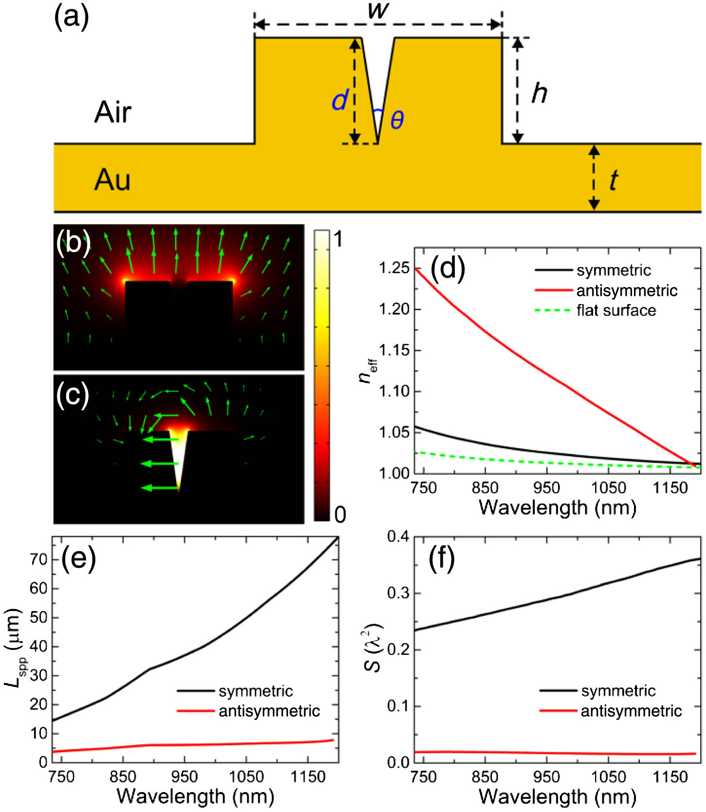
Figure 1.(a) Schematic and geometrical parameters of the multimode plasmonic waveguide. Power flow distributions of the (b) symmetric waveguide mode and (c) antisymmetric waveguide mode for , , , , , and . The green arrows denote the vectors of the electric field. (d) Effective refractive indices, (e) propagation lengths, and (f) field confinements of the symmetric (black lines) as well as antisymmetric (red lines) SPP waveguide modes varying with wavelengths. The green dashed line in (d) denotes the effective refractive indices of the SPP mode on the flat metal surface.
By varying the wavelengths, the modal properties of the plasmonic waveguides are numerically calculated in detail, including the effective refractive indices (), propagation lengths (), and field confinements (). The calculated results are displayed in Figs. 1(d)–1(f). From Fig. 1(d), it is observed that the effective refractive indices of the symmetric SPP waveguide mode are always smaller than that of the antisymmetric SPP waveguide modes because of the different field confinements. The antisymmetric SPP waveguide mode is cut off for because its effective index is smaller than that of the SPP mode on the flat metal surface [green dashed line in Fig. 1(d)] [32,33]. It should be noted that the higher-order mode is also supported by the multimode plasmonic waveguide for . The propagation lengths of the symmetric SPP waveguide mode are larger, and they increase greatly with the increase of the wavelength [black line in Fig. 1(e)], owing to the poor field confinements at long wavelengths [black line in Fig. 1(f)]. However, the propagation lengths of the antisymmetric SPP waveguide mode are much smaller than those of the symmetric waveguide mode because of tight field confinements () [red line in Fig. 1(f)]. In addition, it is observed that the propagation lengths of the antisymmetric SPP waveguide mode increase slowly with the increase of the wavelength, as shown by the red line in Fig. 1(e).
Due to the different field confinements, the bending losses of the two SPP modes are quite different, where is the transmittance of the bending multimode plasmonic waveguide structure. Figure 2(a) shows the schematic of the bending multimode plasmonic waveguide with a radius of , and the inset is its top view. The calculated transmittances of the two SPP waveguide modes in the bending waveguide structure (, , , , and ) at different bending radii and bending angles are displayed in Fig. 2(b) (). Here, the eigenwaveguide modes (symmetric and antisymmetric modes) are set at the incident port in the simulation. It can be seen that the transmittance of the antisymmetric SPP waveguide mode (solid lines) through the bending waveguide structure is greater than that of the symmetric SPP waveguide mode (dashed lines) because of the tight field confinements of the antisymmetric SPP waveguide mode. For the antisymmetric SPP waveguide mode, the propagation loss dominates the bending loss due to the small propagation lengths. With the increase of the bending radius, the transmittance of the antisymmetric SPP waveguide mode decreases because of the increased propagation distance (). However, the transmittance of the symmetric SPP waveguide mode increases slowly with the increase of the bending radius because the radiation loss dominates the bending loss, as shown in Fig. 2(b). For the fixed bending radius, the transmittances of the two SPP modes increase with the decrease of the bending angle. It should be pointed out that the transmittances of the antisymmetric waveguide mode at small bending radii are a little greater than 1.0 because of the mode conversion from the antisymmetric SPP waveguide mode (with a small propagation length of ) to the corner waveguide mode (with a large propagation length of ) [34,35]. To get a large transmittance for the antisymmetric waveguide mode and a small transmittance for the symmetric waveguide mode, the bending angle is chosen to be . The bending radius is chosen to be . In this case, the power flows of the symmetric and antisymmetric waveguide modes above the multimode plasmonic waveguide are displayed in Figs. 2(c) and 2(d). From Fig. 2(c), the symmetric waveguide mode coming from the input multimode plasmonic waveguide is partly converted into the corner mode at the bending waveguide part. The converted corner mode propagates along the outer corners of the bending waveguide, and the transmittance is about 15%. However, the antisymmetric waveguide mode can pass through the bending waveguide with a high transmittance of about 90% because of the tight field confinements, as shown in Fig. 2(d).

Figure 2.(a) Schematic of the bending multimode plasmonic waveguide. (b) Transmittances of the symmetric (dashed lines) and antisymmetric (solid lines) SPP waveguide modes passing through the bending waveguide at different bending radii and bending angles (). Power flow distributions of the (c) symmetric and (d) antisymmetric waveguide modes at and .
Based on different bending losses of the two orthogonal SPP modes, the PBS comprising one bending plasmonic waveguide and one direct-contacting waveguide is designed, as shown in Fig. 3(a). The top view of the designed structure is depicted in Fig. 3(b). The two orthogonal SPP modes coming from the input multimode plasmonic waveguide can be split by the PBS because of the different bending losses. For the antisymmetric SPP waveguide mode, it mainly propagates along the bending waveguide and then is output from Port 2 in the 30° inclined waveguide due to its small bending loss. While, the symmetric SPP waveguide mode coming from the input plasmonic waveguide mainly propagates along the direct-contacting waveguide due to its large bending loss, and it is output from Port 1 in the horizontal waveguide. To efficiently guide the symmetric SPP waveguide mode to propagate along the direct-contacting waveguide, a gap (gap , gap , and gap ) between the bending waveguide and the 30° inclined waveguide is designed. Moreover, in order to improve the extinction ratio, no V-shaped groove is designed in the output horizontal waveguide, and a grating (period of 400 nm) is designed in the outer corners of the output 30° inclined waveguide [32], as shown in Figs. 3(a) and 3(b).
Figure 3.(a) Schematic and (b) top view of the proposed PBS. Power flow distributions of the (c) symmetric and (d) antisymmetric waveguide modes at . Normalized output powers of the (e) symmetric and (f) antisymmetric waveguide modes at different wavelengths in the simulation.
To test the validity of the proposed structure ( and ), the power flows of the symmetric and antisymmetric SPP waveguide modes at are simulated, and the results are shown in Figs. 3(c) and 3(d). It is observed that the symmetric SPP waveguide mode coming from the input multimode plasmonic waveguide mainly goes along the horizontal waveguide, while the antisymmetric waveguide mode coming from the input multimode plasmonic waveguide can pass through the bending waveguide part and mainly propagates along the 30° inclined waveguide. This phenomenon agrees well with the above analysis. The extinction ratio of the symmetric SPP waveguide mode in the polarization splitting process is , and the insertion loss is as low as . For the antisymmetric SPP waveguide mode, the extinction ratio and insertion loss are and , respectively. Furthermore, the normalized output powers of the symmetric and antisymmetric SPP waveguide modes ( and ) at different wavelengths are displayed in Figs. 3(e) and 3(f). In the calculation, the corresponding straight waveguides with the same lengths are used as the reference waveguides for the symmetric and antisymmetric waveguide modes [35,36]. From Fig. 3(e), it is observed that the normalized output power of the symmetric waveguide mode from Port 1 () is much greater than that from Port 2 () from to . However, this phenomenon is just the opposite for the antisymmetric SPP waveguide mode, as shown in Fig. 3(f). As a result, the two orthogonal SPP modes are efficiently split by the proposed structure based on the multimode plasmonic waveguide in a broad bandwidth of about 430 nm. In such a broad bandwidth, the insertion losses are lower than 1.6 dB, and the extinction ratios are greater than 5.0 dB, as shown in Figs. 3(e) and 3(f). From the field distributions in Figs. 3(c) and 3(d), no interference patterns or field enhancements are observed. Moreover, no periodical oscillations or resonant peaks are observed in the response spectra with a large wavelength range from 740 to 1170 nm, as shown in Figs. 3(e) and 3(f). The above phenomena reveal that there is no resonance or interference in the polarization splitting process, which is the reason for the broadband response. Further simulations show that the polarization splitter can work well at for , , , , and . This large structural tolerance coincides with the broad bandwidth of the proposed polarization splitter. It should be pointed out that the above simulation aims mainly in the central wavelength of 900 nm because of the response of the CMOS and the propagation loss of the SPPs. However, the working mechanism can be extended to the telecom wavelength (), and the simulation shows that the performances of the polarization splitter around are comparable to that around .
3. EXPERIMENT AND RESULTS
Next, we further verify our proposal in the experiment. The proposed structure based on the multimode plasmonic waveguide in Fig. 3(a) is fabricated by focused ion beams (FIBs) in a 450 nm thick gold film. The gold film with a 30 nm thick titanium adhesion layer is deposited on a glass substrate by magnetron sputtering. Compared with the complex hybrid plasmonic structure, the simple bending multimode plasmonic waveguide is much easier to fabricate. Figure 4(a) displays the scanning electron microscopy (SEM) image of the fabricated structure, which comprises the proposed PBS (green dashed rectangle), one input waveguide, one output horizontal waveguide, and one output 30° inclined waveguide. The measured bending radius and bending angle are about and , respectively. The period of the reflected grating is about 400 nm. Hence, the footprint of the PBS is only about , as shown by the green dashed rectangle in Fig. 4(a). This footprint is comparable to that in the previous experimental reports [5,35]. To excite two SPP modes, a grating with a period of about 740 nm is etched on the input waveguide, as shown in Fig. 4(a). The separation between the excited grating and the bending waveguide is about 8 μm. Two decoupling gratings (period of about 740 nm) are fabricated on the horizontal waveguide and the 30° inclined waveguide [Fig. 4(a)] to scatter the SPP modes to the free space for the far-field detection. To observe the cross section of the waveguide, the structure is etched by the ion beam, and the cross section of the multimode plasmonic waveguide is shown in Fig. 4(b). This FIB etching has damage to the bottom of the V-shaped groove. Moreover, the spattering gold particles in the FIB etching partly stack on the bottom of the V-shaped groove. Hence, the SEM image after the FIB etching cannot reflect the real corner at the bottom of the V-shaped groove, and the radius of the V-shaped groove corner cannot be actually measured based on the SEM image in Fig. 4(b). The other structure parameters of the multimode plasmonic waveguide are measured to be , , , and . From Fig. 4(b), the roughness on the surface of the V-shaped groove is very small. When the roughness of the V-shaped groove surface is 5 nm (or 10 nm), the simulation shows that the propagation length of the antisymmetric mode decreases by only about 3% (12%). This small decrease (from to ) has little effect on the device performance.
Figure 4.(a) SEM image of the fabricated structures. (b) Cross-sectional SEM image of the multimode plasmonic waveguide. CMOS captured pictures under (c), (e), (g) p-polarized and (d), (f), (h) s-polarized incident light at different wavelengths. The red dashed rectangles in (c)−(h) denote the decoupling gratings.
In the optical measurement, a monochromatic light is filtered from a supercontinuum light source (Fianium) by an acoustic optical tunable filter. The polarization of the monochromatic light is controlled by a half-wave plate and a Glan–Taylor prism. Then, the incident light is focused on the excited grating from the front side by an objective (Olympus , ), and the focused spot diameter is about 1.5 μm. The symmetric and asymmetric SPP waveguide modes can be excited by the p- and s-polarized incident light, respectively [32]. The two SPP waveguide modes propagate along the plasmonic waveguide until being scattered by the decoupling grating. The scattered light is collected by the same objective (Olympus , ) and then imaged by a lens () onto a CMOS. The captured optical images for the symmetric and antisymmetric SPP waveguide modes at three typical wavelengths are displayed in Figs. 4(c)–4(h). It should be pointed out that the incident power, integration time, and CMOS response at different wavelengths [Figs. 4(c)–4(h)] are not the same. Under the p-polarized incident light [Figs. 4(c), 4(e), and 4(g)], the symmetric SPP waveguide mode is excited by the excited grating, and the decoupling grating on the output horizontal waveguide is much brighter than that on the output inclined one. This phenomenon indicates that the excited symmetric waveguide mode mainly propagates along the horizontal waveguide. On the contrary, the decoupling grating on the output inclined waveguide is much brighter than that on the output horizontal one under the s-polarized incident light [Figs. 4(d), 4(f), and 4(h)], indicating that the excited antisymmetric waveguide mode mainly goes along the 30° inclined waveguide. Therefore, the symmetric and antisymmetric SPP modes guided by the input multimode plasmonic waveguide are efficiently split by the proposed structure. It should be noted that the p-polarization has consistently stronger intensity than the s-polarization. The reason is that the propagation length of the antisymmetric mode () is much smaller than that of the symmetric mode (). At , the extinction ratios are calculated to be about 6.3 and 12.5 dB for the symmetric and antisymmetric waveguide modes, respectively, and the corresponding insertion losses are as low as about 0.7 and 0.9 dB, respectively, which are much smaller than that in the previous experimental works [23,25,26,32,35].
To quantificationally investigate the performance of the proposed PBS, the normalized powers of the scattered light from the decoupling gratings are measured at different wavelengths for the p- and s-polarized incident light, and the results are displayed in Figs. 5(a) and 5(b). Here, to exclude the differences (incident power, integration time, and CMOS response), the reference samples are used to normalize the scattered powers. For the p-polarized incident light, the normalized powers of the scattered light from the decoupling grating on the output horizontal waveguide are much greater than that on the output inclined waveguide in the wavelength range from 750 to 1000 nm, as shown in Fig. 5(a). This agrees well with the simulation results [Fig. 3(e)], indicating that the excited symmetric SPP waveguide mode mainly propagates along the horizontal waveguide. For the s-polarized incident light, the normalized powers of the scattered light from the decoupling grating on the output inclined waveguide are much greater than that on the output horizontal waveguide in the wavelength range from 870 to 1000 nm, as shown in Fig. 5(b). This agrees well with the simulation results [Fig. 3(f)], indicating that the excited antisymmetric SPP waveguide mode mainly propagates along the inclined waveguide. However, for the small wavelengths (), the normalized powers of the scattered light from the decoupling grating on the output inclined waveguide are smaller than that on the output horizontal waveguide [Fig. 5(b)]. This deviation from the simulation results [Fig. 3(f)] stems from the appearance of the higher-order mode at the short wavelengths because of the increased groove depth and decreased angle of the V-shaped groove in the experiment.
Figure 5.Measured normalized scattered powers under (a) p-polarized and (b) s-polarized incident light at different wavelengths. (c) Power flow distribution of the higher-order mode at . The green arrows denote the vectors of the electric field. (d) Effective indices of the symmetric (black line), antisymmtric (red line) and higher-order (blue line) modes at different wavelengths. The green dashed line in (d) shows the effective indices of the SPP mode on the flat metal surface.
The properties of the SPP mode in the real experimental waveguide (, , , and radius of round corners of the waveguide being 50 nm) are simulated. It is found that the higher-order mode are supported at , as shown in Fig. 5(c). Moreover, the effective refractive indices of the SPP modes in the plasmonic waveguide at different wavelengths are calculated, as shown in Fig. 5(d). Besides the symmetric (black line) and antisymmetric (red line) SPP modes, the higher-order SPP mode is also supported for short wavelengths, as shown by the blue line in Fig. 5(d). With the increase of the corner radius and angle of the V-shaped groove, the cutoff wavelength of the higher-order mode decreases. Here, the radius of the V-shaped groove corner of is estimated by the cutoff wavelength of the higher-order mode.
Based on the distribution of the electric vector [green arrows in Fig. 5(c)], the higher-order mode can be excited by the s-polarized incident light. More importantly, a part of power flows of the higher-order mode are distributed in the outer corners of the waveguide. As a result, the higher-order mode can be easily converted to the symmetric mode in the horizontal waveguide when it passes the bending part [34,37]. Because of the mode conversion and the small propagation loss of the symmetric mode, the output normalized power from Port 2 () is smaller than that from Port 1 () for short wavelengths (). In the wavelength range from 870 to 990 nm, the insertion losses are both lower than 3 dB for the symmetric and antisymmetric modes, and the minimum insertion loss is as low as 0.7 dB, as shown in Figs. 5(a) and 5(b). This insertion loss is smaller than that in the previous experimental works [23,25,26,32,35]. Hence, there is a broad 3 dB bandwidth of about 120 nm in the proposed PBS [3,38], in which the extinction ratios are greater than 5.0 dB. This bandwidth () is much greater than that () by using the bending hybrid plasmonic waveguide [35], which is recently reported by our group. The reason is that the antisymmetric SPP mode is tightly confined for any wavelengths, as shown in Fig. 1(f). The maximum extinction ratio can be up to about 12.5 dB, which is comparable to that in the previous experimental works [23,35]. By further improving the design of the plasmonic structure, the extinction ratio can be increased. For example, the extinction ratio of the symmetric mode can be improved by increasing the length of the reflected grating in the inclined waveguide. The extinction ratio of the antisymmetric mode can be improved by designing a gap [35] or blocking wall between the output horizontal waveguide and the bending waveguide.
4. CONCLUSION
In summary, by using the bending multimode plasmonic waveguide, an ultrabroadband on-chip PBS with low insertion losses was experimentally demonstrated. Herein, the proposed multimode plasmonic waveguide could support both the symmetric and antisymmetric waveguide modes. Due to the different field distributions, the bending losses of the two SPP waveguide modes were quite different. Consequently, the antisymmetric waveguide mode mainly passed through the bending multimode plasmonic waveguide and propagated along the inclined waveguide, while the symmetric waveguide mode mainly propagated along the horizontal waveguide. In addition, there is no resonant or interference effect in the splitting process, which greatly broadened the operating bandwidth of the PBS to about 430 nm (insertion loss and extinction ratio ) in theory. In the experiment, an ultrabroadband (about 120 nm) PBS was realized. Moreover, since the strongly confined waveguide modes instead of the bulk free-space light were utilized as the incident sources, the insertion losses were greatly decreased to be smaller than 3 dB (with the minimum insertion loss of 0.7 dB). Such an ultrabroadband on-chip plasmonic PBS with low insertion losses would find important applications in the PICs.
References
[1] T. Barwicz, M. R. Watts, M. A. Popović, P. T. Rakich, L. Socci, F. X. Kärtner, E. P. Ippen, H. I. Smith. Polarization-transparent microphotonic devices in the strong confinement limit. Nat. Photonics, 1, 57-60(2007).
[2] D. Dai, J. Bauters, J. E. Bowers. Passive technologies for future large-scale photonic integrated circuits on silicon: polarization handling, light non-reciprocity and loss reduction. Light Sci. Appl., 1, e1-e12(2012).
[3] D. Dai, L. Liu, S. Gao, D. X. Xu, S. He. Polarization management for silicon photonic integrated circuits. Laser Photon. Rev., 7, 303-328(2013).
[4] A. Y. Piggott, J. Lu, K. G. Lagoudakis, J. Petykiewicz, T. M. Babinec, J. Vučković. Inverse design and demonstration of a compact and broadband on-chip wavelength demultiplexer. Nat. Photonics, 9, 374-377(2015).
[5] B. Shen, P. Wang, R. Polson, R. Menon. An integrated-nanophotonics polarization beamsplitter with 2.4 × 2.4 μm2 footprint. Nat. Photonics, 9, 378-382(2015).
[6] S. Lin, J. Hu, K. B. Crozier. Ultracompact, broadband slot waveguide polarization splitter. Appl. Phys. Lett., 98, 151101(2011).
[7] D. Dai, Z. Wang, J. E. Bowers. Ultrashort broadband polarization beam splitter based on an asymmetrical directional coupler. Opt. Lett., 36, 2590-2592(2011).
[8] B.-K. Yang, S.-Y. Shin, D. Zhang. Ultrashort polarization splitter using two-mode interference in silicon photonic wires. IEEE Photon. Technol. Lett., 21, 432-434(2009).
[9] A. Hosseini, S. Rahimi, X. Xu, D. Kwong, J. Covey, R. Chen. Ultracompact and fabrication-tolerant integrated polarization splitter. Opt. Lett., 36, 4047-4049(2011).
[10] Z. Su, E. Timurdogan, E. S. Hosseini, J. Sun, G. Leake, D. D. Coolbaugh, M. R. Watts. Four-port integrated polarizing beam splitter. Opt. Lett., 39, 965-968(2014).
[11] M. Watts, H. Haus, E. Ippen. Integrated mode-evolution-based polarization splitter. Opt. Lett., 30, 967-969(2005).
[12] L. Augustin, R. Hanfoug, J. Van der Tol, W. De Laat, M. Smit. A compact integrated polarization splitter/converter in InGaAsP–InP. IEEE Photon. Technol. Lett., 19, 1286-1288(2007).
[13] D. Dai, Z. Wang, J. E. Bowers. Considerations for the design of asymmetrical Mach–Zehnder interferometers used as polarization beam splitters on a submicrometer silicon-on-insulator platform. J. Lightwave Technol., 29, 1808-1817(2011).
[14] X. Ao, L. Liu, L. Wosinski, S. He. Polarization beam splitter based on a two-dimensional photonic crystal of pillar type. Appl. Phys. Lett., 89, 171115(2006).
[15] D. K. Gramotnev, S. I. Bozhevolnyi. Plasmonics beyond the diffraction limit. Nat. Photonics, 4, 83-91(2010).
[16] W. Wang, Q. Yang, F. Fan, H. Xu, Z. L. Wang. Light propagation in curved silver nanowire plasmonic waveguides. Nano Lett., 11, 1603-1608(2011).
[17] M. Cohen, Z. Zalevsky, R. Shavit. Towards integrated nanoplasmonic logic circuitry. Nanoscale, 5, 5442-5449(2013).
[18] C.-L. Zou, F.-W. Sun, C.-H. Dong, X.-F. Ren, J.-M. Cui, X.-D. Chen, Z.-F. Han, G.-C. Guo. Broadband integrated polarization beam splitter with surface plasmon. Opt. Lett., 36, 3630-3632(2011).
[19] Q. Tan, X. Huang, W. Zhou, K. Yang. A plasmonic based ultracompact polarization beam splitter on silicon-on-insulator waveguides. Sci. Rep., 3, 2206(2013).
[20] F. Lou, D. Dai, L. Wosinski. Ultracompact polarization beam splitter based on a dielectric-hybrid plasmonic-dielectric coupler. Opt. Lett., 37, 3372-3374(2012).
[21] X. Guan, H. Wu, Y. Shi, D. Dai. Extremely small polarization beam splitter based on a multimode interference coupler with a silicon hybrid plasmonic waveguide. Opt. Lett., 39, 259-262(2014).
[22] L. Gao, F. Hu, X. Wang, L. Tang, Z. Zhou. Ultracompact and silicon-on-insulator-compatible polarization splitter based on asymmetric plasmonic-dielectric coupling. Appl. Phys. B, 113, 199-203(2013).
[23] J. Chee, S. Zhu, G. Lo. CMOS compatible polarization splitter using hybrid plasmonic waveguide. Opt. Express, 20, 25345-25355(2012).
[24] K. W. Chang, C. C. Huang. Ultrashort broadband polarization beam splitter based on a combined hybrid plasmonic waveguide. Sci. Rep., 6, 19609(2016).
[25] J. Chen, C. Sun, H. Li, Q. Gong. Experimental demonstration of an on-chip polarization splitter in a submicron asymmetric dielectric-coated metal slit. Appl. Phys. Lett., 104, 231111(2014).
[26] C. Sun, H. Li, Q. Gong, J. Chen. Ultra-small and broadband polarization splitters based on double-slit interference. Appl. Phys. Lett., 108, 101106(2016).
[27] P. B. Johnson, R. W. Christy. Optical constants of the noble metals. Phys. Rev. B, 6, 4370-4379(1972).
[28] S. I. Bozhevolnyi, V. S. Volkov, E. Devaux, T. W. Ebbesen. Channel plasmon-polariton guiding by subwavelength metal grooves. Phys. Rev. Lett., 95, 046802(2005).
[29] S. I. Bozhevolnyi, V. S. Volkov, E. Devaux, J. Y. Laluet, T. W. Ebbesen. Channel plasmon subwavelength waveguide components including interferometers and ring resonators. Nature, 440, 508-511(2006).
[30] V. S. Volkov, S. I. Bozhevolnyi, S. G. Rodrigo, L. Martin-Moreno, F. J. García-Vidal, E. Devaux, T. W. Ebbesen. Nanofocusing with channel plasmon polaritons. Nano Lett., 9, 1278-1282(2009).
[31] E. Moreno, F. Garcia-Vidal, S. G. Rodrigo, L. Martin-Moreno, S. I. Bozhevolnyi. Channel plasmon-polaritons: modal shape, dispersion, and losses. Opt. Lett., 31, 3447-3449(2006).
[32] F. Gan, C. Sun, Y. Wang, H. Li, Q. Gong, J. Chen. Multimode metallic double-strip waveguides for polarization manipulation. Adv. Mater. Technol., 2, 1600248(2017).
[33] C. Sun, K. Rong, Y. Wang, H. Li, Q. Gong, J. Chen. Plasmonic ridge waveguides with deep-subwavelength outside-field confinements. Nanotechnology, 27, 065501(2016).
[34] D. Dai, J. E. Bowers. Novel concept for ultracompact polarization splitter-rotator based on silicon nanowires. Opt. Express, 19, 10940-10949(2011).
[35] C. Sun, K. Rong, F. Gan, S. Chu, Q. Gong, J. Chen. An on-chip polarization splitter based on the radiation loss in the bending hybrid plasmonic waveguide structure. Appl. Phys. Lett., 111, 101105(2017).
[36] Y. H. Ding, H. Y. Ou, C. Peucheret. Wideband polarization splitter and rotator with large fabrication tolerance and simple fabrication process. Opt. Lett., 38, 1227-1229(2013).
[37] D. Dai, J. Wang, S. He. Silicon multimode photonic integrated devices for on-chip mode-division-multiplexed optical interconnects. Prog. Electromagn. Res., 143, 773-819(2013).
[38] Y. Tang, D. Dai, S. He. Proposal for a grating waveguide serving as both a polarization splitter and an efficient coupler for silicon-on-insulator nanophotonic circuits. IEEE Photon. Technol. Lett., 21, 242-244(2009).


