Abstract
We demonstrate an integrated Si optical single-sideband (OSSB) modulator composed of a parallel dual-ring modulator (PDRM) and a quadrature hybrid coupler (QHC). Both the PDRM and the QHC are carefully designed for 30 GHz opearation, and their operations are verified by measurement. The Si OSSB modulator successfully generates a single sideband with larger than 15 dB suppression of the undesired sideband.1. INTRODUCTION
Optical single-sideband (OSSB) modulation eliminates the frequency-dependent power fading problem from which optical double-sideband (ODSB) modulation suffers when high-frequency signals are delivered in the optical domain over dispersive fiber for radio-over-fiber (RoF) applications [1,2]. OSSB modulation is essential for realizing high-performance RoF links, especially for millimeter-wave wireless networks, which with their higher carrier frequencies suffer more from the power fading problem [3]. OSSB modulation also allows higher spectral efficiency for dense WDM transmission systems [4]. OSSB modulation can be achieved by eliminating the undesired sideband with optical notch filters based on, for example, fiber Bragg gratings [5] or stimulated Brillouin scattering [6]. However, these techniques require highly selective optical filters whose characteristics may not be robust enough for practical applications. OSSB modulation has also been realized with a Mach–Zehnder modulator (MZM) [2,7–11]. Various MZM configurations have been used, including a dual-electrode MZM [2,7], a dual-parallel MZM [7,8], and an MZM cascaded with a phase modulator [9]. In addition, there have been extensive investigations for the ring-assisted MZM [10–13] and, using this, OSSB modulation has been demonstrated [14,15]. Although these techniques can produce high-quality OSSB signals, their implementation requires several different pieces of optical and electrical components, resulting in limited practical applicability.
In this paper, we demonstrate for the first time, to the best of our knowledge, a single-chip Si OSSB modulator operating in the millimeter-wave range of 30 GHz. Our OSSB modulator includes an optical modulator and a 30-GHz I/Q signal generator, both of which are integrated on a Si wafer. Such monolithic integration of photonic and electronic components results in much smaller sizes and, consequently, significant cost reduction; it provides great advantages for many applications. Our OSSB modulator is fabricated with IHP’s Photonic BiCMOS technology, which provides high-performance Si photonic devices and Si BiCMOS circuits on the standard Si platform [16].
This paper is organized as follows. In Section 2, the structure of our OSSB modulator is explained and the characteristics of the depletion-type microring modulators (MRMs) used within the OSSB modulator are given. In Section 3, the lumped-element quadrature hybrid coupler (QHC) [17] is described, which is used for generating electrical I/Q signals around 30 GHz having the same magnitude with a 90° phase difference. In Section 4, the measured OSSB modulation characteristics are given. Section 5 concludes the paper. An initial result of this work has been presented in Ref. [18].
Sign up for Photonics Research TOC. Get the latest issue of Photonics Research delivered right to you!Sign up now
2. OSSB MODULATOR STRUCTURE
Figure 1 shows the block diagram of our OSSB modulator composed of a parallel dual-ring modulator (PDRM) and a QHC and schematically explains how OSSB signals are produced. The input light having angular frequency is supplied into one input port of a multi-mode interferometer (MMI). Each of two MMI outputs having a 90° optical phase difference [19] is delivered into the identical MRM located on the top and bottom arms. Electrical sinusoidal signals having angular frequency are applied to the QHC, which produces two electrical output signals having the same magnitude but a 90° electrical phase difference. When one of the QHC output signals is used for modulating the top MRM and the other the bottom MRM, there exists a 180° optical phase difference between one of the two sidebands of the modulated optical signals in the top and bottom arms (lower sideband in the case of Fig. 1). When these are summed in a output MMI, the output optical signal has only one sideband thus achieving OSSB modulation. Our OSSB modulator is implemented with a PDRM instead of the standard MZM since the PDRM provides the much smaller device size.
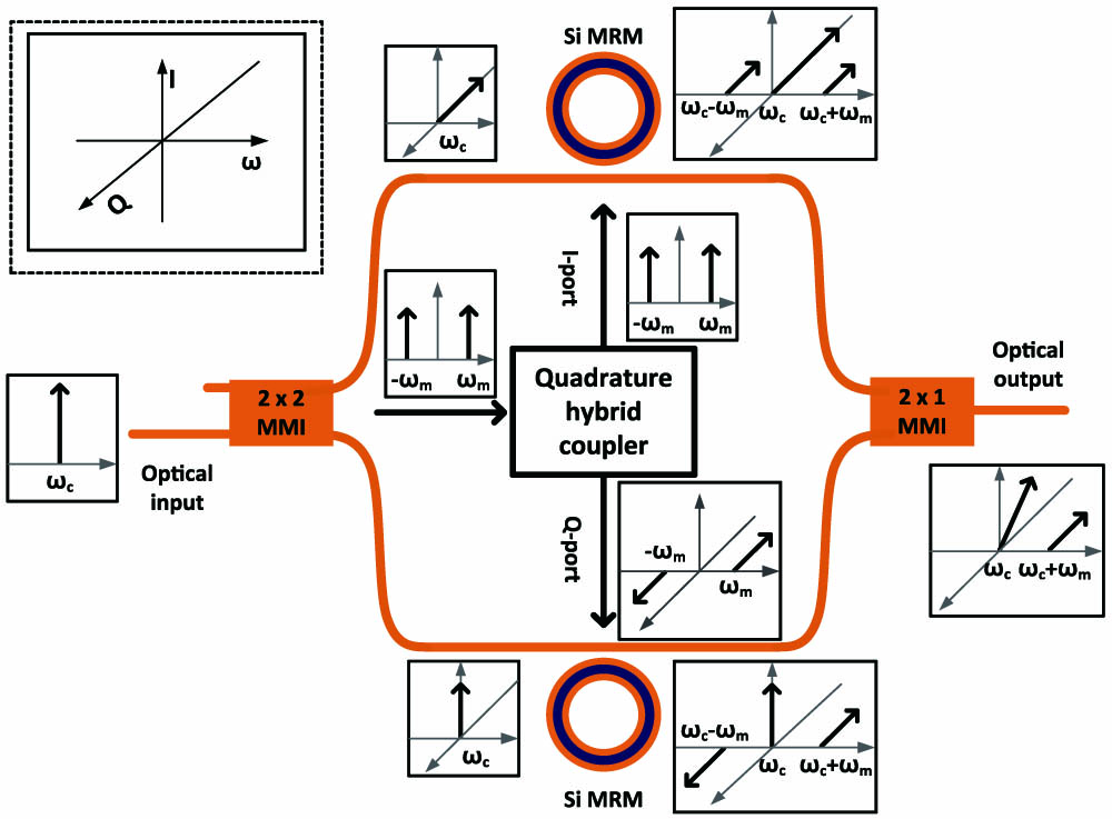
Figure 1.Block diagram of the OSSB modulator.
Figure 2 shows a microphotograph of the fabricated Si OSSB modulator. Its core size is ( for the QHC and for the PDRM). Grating couplers (not shown in the figure) are used for the PDRM input and output optical coupling, and GSG pads shown on the left are used for supplying electrical sinusoidal signals to the QHC. The top DC pads are used for ground connection (G), tuning varactors within the QHC (), and supplying bias voltages to MRMs (). The bottom DC pads are used for ground connection (G) and MRM heater control (). Other DC pads are not used for the present investigation.

Figure 2.Microphotograph of the integrated Si OSSB modulator.
Figure 3(a) shows the structure of two identical MRMs within the PDRM. It has a ring radius of 11 μm and a coupling gap of 280 nm. The ring waveguide is 500 nm wide and 220 nm thick and has a PN junction whose nominal peak doping concentrations are for P-doping and for N-doping. For and regions, nominal doping concentrations of are used.
Figure 3.(a) Structure and (b) cross section and the electrical model of the Si MRM.
Since the resonance wavelength of two MRMs within the PDRM may not be the same due to process variations, each MRM has an on-chip heater made up of an N-doped Si layer, as shown in Fig. 3(a), so that its resonance wavelength can be externally tuned. For QHC implementation, the precise electrical characteristics of the MRM are needed, as will be explained in Section 3. Figure 3(b) shows the MRM cross section along with its electrical equivalent circuit model [20]. and represent the capacitance of the 2 μm BOX oxide between N-doped and P-doped regions and the substrate, is the substrate resistance, is the PN junction capacitance, and and are the series resistance for N-doped and P-doped regions of the rib waveguide, respectively. The numerical values for these electrical parameters can be extracted by electrical measurement of a MRM device. Figures 4(a) and 4(b) show magnitude and phase measurement results obtained from a stand-alone MRM device fabricated for the testing purpose and having the identical structure as two MRMs within the PDRM. Also shown are the simulated results carried out with the exacted parameters whose values are shown in Table 1.
| Parameter | Value |
| Rs(=Rn+Rp) | 220 Ω |
| Cj | 10.5 fF |
| Cox(=Cn+Cp) | 8.5 fF |
| Rsub | 4.2 kΩ |
Table 1. Numerical Values for MRM Electrical Parameters
Figure 4.Measured and simulated electrical (a) magnitude and (b) phase of the Si MRM. For simulation, extracted values shown in Table 1 are used.
Figure 5 shows the measured optical transmission spectra at three different bias voltages for the same MRM device. It has the resonance wavelength tunability of 27 pm/V, the ring round-trip loss () of 0.957, the through coefficient () of 0.957, and the effective refractive index () of 2.5224, determined using the extraction technique reported in Ref. [20]. With these, the MRM modulation characteristics can be precisely predicted [21]. Figure 6(a) shows the simulated normalized MRM modulation frequency responses at a bias voltage of for several different values of , defined as the difference between the resonance wavelength and the input light wavelength, as shown in the inset of Fig. 6(a). The MRM modulation characteristics strongly depend on [22] and, consequently, for our investigation, is carefully determined by simulation and confirmed by measurement for optimal performance for the target modulation frequency. Figure 6(b) shows the normalized measured and simulated optical spectra when the test MRM device is modulated with 30 GHz, 2 Vpp sinusoidal signals with . The measured and the simulated results agree well, except that the measured results have a much higher baseline due to noise in the measurement and much larger linewidth mostly due to the limited resolution of the optical spectrum analyzer used for the measurement. The second-order modulation peak can be observed in the right side, which is due to nonlinear modulation characteristics of the MRM [23].
Figure 5.Measured optical transmission spectra of the Si MRM at different bias voltages.
Figure 6.(a) Simulated modulation frequency response and (b) measured and simulated optical spectrum for Si MRM modulated at 30 GHz with .
3. QHC
The QHC is often implemented with transmission lines [24], but the requiring size is too large for our consideration. Instead, we implemented our QHC with inductors and capacitors [25] in order to minimize its size. Figure 7 shows its structure.
Figure 7.Schematic of the QHC.
For the desired QHC operation at frequency , , , and , where should be satisfied when is 50 Ω [26]. However, cannot be satisfied for our MRMs. We can determine MRM at a given frequency with the MRM equivalent circuit shown in Fig. 3(b), and its parameter values are given in Table 1. With this, the required and values for the QHC when it is loaded with MRMs can be determined by simulation. Figures 8(a) and 8(b) show the simulated magnitude of and the phase difference between two QHC output signals when it is loaded with two MRMs. For the simulation, the and values shown in Table 2 are used. Around 30 GHz, the magnitudes of two output signals are almost identical with an insertion loss of about 8 dB and have 90° phase difference. For implementation, and are realized with spiral inductors, with MIM capacitors, and with varactors, all of which IHP’s Photonic BiCMOS technology provides. Varactors are used so that the capacitances can be externally tuned in case process variation causes variances in circuit parameters. With the bias voltage ranging from 0.5 to , the capacitance of each varactor changes from 8 to 3 fF. For externally tuning the varactors, four varactors are grouped into two pairs ( and , and ) and each pair is tuned together in order to reduce tuning complexity.
| Parameter | Value |
| L1 | 580 pH |
| L2 | 410 pH |
| C | 97 fF |
Table 2. and Values Used for QHC Implementation
Figure 8.Simulated (a) magnitude of and (b) phase difference between I/Q output signals for the QHC with Si MRM loads.
In order to confirm the accuracy of our QHC design, a stand-alone QHC, which is identical with the QHC used in the OSSB modulator but without MRM loads is fabricated, and its -parameters are measured with 50 Ω loads provided by a network analyzer. Figures 9(a) and 9(b) show that measured and simulated results agree very well. For simulation, the parameter values given in Table 2 are used.
Figure 9.Measured and simulated for (a) magnitude of and (b) phase difference between QHC I/Q output signals with 50 Ω loads.
4. OSSB MODULATOR CHARACTERISTICS
Figure 10(a) shows the output transmission spectrum around 1546 nm of our PDRM. As can be seen, its resonance peak is significantly broadened. This is due to the mismatch between two MRMs caused by slight process nonuniformity. Such mismatch significantly degrades the PDRM modulation efficiency. This problem can be solved by heating up one of the MRMs so that they have the identical resonance wavelength. Figure 10(b) shows the resulting output transmission spectra of the same PDRM at three different bias voltages when one MRM is heated up about 1.7°C. As can be seen, the resonance peak broadening is eliminated. In addition, a resonance wavelength tunability of 27 pm/V is observed. Figure 10(c) shows the measured optical spectrum of the OSSB modulator output when it is modulated with 30 GHz, 2 Vpp electrical sinusoidal signals and . OSSB modulation is successfully achieved with larger than 15 dB suppression of the undesired sideband. Our grating coupler has about 5 dB coupling loss, resulting in 10 dB loss for the modulator input and output coupling. The MRM has about 6 dB loss when . Each of two MMIs used in our OSSB modulator has about 1 dB loss. Consequently, the total insertion loss is about 18 dB.
Figure 10.Measured optical transmission spectra of the PDRM (a) without temperature control and zero bias voltage and (b) with temperature control at three different bias voltages. (c) Measured OSSB modulator output optical spectrum when modulated with 30 GHz, 2 Vpp sinusoidal signals at and 1 V bias voltage.
Figure 11 shows the measured optical spectra of the OSSB modulator output when the modulation frequency varies from 28 to 32 GHz. The upper sideband spectra are enlarged in the inset. As shown in the figure, our OSSB modulator can operate in a wide range of modulation frequencies, making it suitable for many millimeter-wave applications having large bandwidth.
Figure 11.Measured output spectra of the OSSB modulator with different modulation frequencies.
5. CONCLUSION
We successfully demonstrate a monolithically integrated 30 GHz Si OSSB modulator that contains a PDRM and an electrical I/Q signal generator. Each built-in component in our electronic–photonic integrated circuit is carefully designed and implemented. Our OSSB modulator achieves larger than 15 dB suppression of the undesired sideband. This Si OSSB modulator should provide great advantages in its size and cost for many applications requiring OSSB operation.
References
[1] G. H. Smith, D. Novak, Z. Ahmed. Technique for optical SSB generation to overcome dispersion penalties in fiber-radio systems. Electron. Lett., 33, 74-75(1997).
[2] M. Y. Frankel, R. D. Esman. Optical single-sideband suppressed-carrier modulator for wide-band signal processing. J. Lightwave Technol., 16, 859-863(1998).
[3] U. Gliese, S. Norskov, T. N. Nielsen. Chromatic dispersion in fiber-optic microwave and millimeter-wave links. IEEE Trans. Microw. Theory Tech., 44, 1716-1724(1996).
[4] M. J. Sieben. Single sideband modulation for digital fiber optic communication systems(1998).
[5] J. Park, W. V. Sorin, K. Y. Lau. Elimination of the fiber chromatic dispersion penalty on 1550 nm millimitre-wave optical transmission. Electron. Lett., 33, 512-513(1997).
[6] Y. Shen, X. Zhang, K. Chen. Optical single sideband modulation of 11-GHz RoF system using stimulated Brillouin scattering. IEEE Photon. Technol. Lett., 17, 1277-1279(2005).
[7] Y. Ogiso, Y. Tsuchiya, S. Shinada, S. Nakajima, T. Kawanishi, H. Nakajima. High extinction-ratio integrated Mach–Zehnder modulator with active Y-branch for optical SSB signal generation. IEEE Photon. Technol. Lett., 22, 941-943(2010).
[8] M. Izutsu, S. Shikama, T. Sueta. Integrated optical SSB modulator/frequency shifter. IEEE J. Quantum Electron., 17, 2225-2227(1981).
[9] B. Davies, J. Conradi. Hybrid modulator structures for subcarrier and harmonic subcarrier optical single sideband. IEEE Photon. Technol. Lett., 10, 600-602(1998).
[10] P. Dong, C. Xie, L. L. Buhl, Y.-K. Chen. Silicon microring modulators for advanced modulation formats. Proceedings of Optical Fiber Communication Conference (OFC), OW4J.2(2013).
[11] C.-M. Chang, G. Valicourt, S. Chandrasekhar, P. Dong. Differential microring modulators for intensity and phase modulation: theory and experiment. J. Lightwave Technol., 35, 3116-3124(2017).
[12] R. Li, D. Patel, A. Samani, E. E. El-Fiky, Z. Xing, M. Morsy-Osman, D. V. Plant. Silicon photonic ring-assisted MZI for 50 Gb/s DAC-less and DSP-free PAM-4 transmission. IEEE Photon. Technol. Lett., 29, 1046-1049(2017).
[13] R. Li, D. Patel, E. E. El-Fiky, A. Samani, Z. Xing, M. M. Morsy-Osman, D. V. Plant. High-speed low-chirp PAM-4 transmission based on push-pull silicon photonic microring modulators. Opt. Express, 25, 13222-13229(2017).
[14] A. M. Gutierrez, J. V. Galan, J. Herrera, A. Brimont, D. Marris-Morini, J.-M. Fédéli, L. Vivien, P. Sanchis. High-linear ring-assisted MZI electro-optic silicon modulators suitable for radio-over-fiber applications. IEEE International Conference on Group IV Photonics, 57-59(2012).
[15] X. Xie, J. Khurgin, J. Kang, F.-S. Chow. Linearized Mach–Zehnder intensity modulator. IEEE Photon. Technol. Lett., 15, 531-533(2003).
[16] L. Zimmermann, D. Knoll, M. Kroh, S. Lischke, D. Petousi, G. Winzer, Y. Yamamoto. BiCMOS silicon photonics platform. Proceedings of Optical Fiber Communication Conference, Th4E.5(2015).
[17] E. A. Fardin, A. S. Holland, K. Ghorbani. Electronically tunable lumped element 90° hybrid coupler. Electron. Lett., 42, 353-355(2006).
[18] B.-M. Yu, J.-M. Lee, C. Mai, S. Lischke, L. Zimmermann, W.-Y. Choi. A monolithically integrated Si optical single-sideband modulator. Fourteenth International Workshop on IEEE International Conference on Group IV Photonics(2017).
[19] K. Kojima, W. Yuan, B. Wang, T. Koike-Akino, K. Parsons, S. Nishikawa, E. Yagyu. An MMI-based polarization splitter using patterned metal and tilted joint. Opt. Express, 20, B371-B376(2012).
[20] B.-M. Yu, J.-M. Lee, Y. Ban, S.-H. Cho, W.-Y. Choi. Model parameter extraction for Si micro-ring modulators. Optoelectronics and Communication Conference and the Australian Conference on Optical Fiber Technology (OECC/ACOFT)(2014).
[21] M. Shin, Y. Ban, B.-M. Yu, M.-H. Kim, J. Rhim, L. Zimmermann, W.-Y. Choi. A linear equivalent circuit model for depletion-type silicon microring modulators. IEEE Trans. Electron Devices, 64, 1140-1145(2017).
[22] J. Müller, F. Merget, S. S. Azadeh, J. Hauck, S. Romero García, B. Shen, J. Witzens. Optical peaking enhancement in high-speed ring modulators. Sci. Rep., 4, 6310(2014).
[23] A. Ayazi, T. Baehr-Jones, Y. Liu, A. E. J. Lim, M. Hochberg. Linearity of silicon ring modulators for analog optical links. Opt. Express, 20, 13115-13122(2012).
[24] J. Lange. Interdigitated stripline quadrature hybrid. IEEE Trans. Microw. Theory Tech., 17, 1150-1151(1969).
[25] Y. C. Chiang, C.-Y. Chen. Design of a wide-band lumped-element 3-dB quadrature coupler. IEEE Trans. Microw. Theory Tech., 49, 476-479(2001).
[26] I. Bahl. Lumped Elements for RF and Microwave Circuits(2003).


