Abstract
Dielectric metasurfaces have achieved great success in realizing high-efficiency wavefront control in the optical and infrared ranges. Here, we experimentally demonstrate several efficient, polarization-independent, all-silicon dielectric metasurfaces in the terahertz regime. The metasurfaces are composed of cylindrical silicon pillars on a silicon substrate, which can be easily fabricated using etching technology for semiconductors. By locally tailoring the diameter of the pillars, full control over abrupt phase changes can be achieved. To show the controlling ability of the metasurfaces, an anomalous deflector, three Bessel beam generators, and three vortex beam generators are fabricated and characterized. We also show that the proposed metasurfaces can be easily combined to form composite devices with extended functionalities. The proposed controlling method has promising applications in developing low-loss, ultra-compact spatial terahertz modulation devices.1. INTRODUCTION
Metasurfaces, which are 2D versions of metamaterials, overcome many drawbacks of 3D metamaterials, such as their complicated design and fabrication challenges, as well as their large material loss. Metasurfaces are generally composed of subwavelength scatterers patterned on planar interfaces, which can control the phase, polarization, amplitude, and, thus, the complex field distribution of the transmitted or reflected electromagnetic wave in a flexible way [1,2]. The flat, ultrathin, and easy-to-fabricate features make metasurfaces promising for next-generation compact photonic devices [3–9]. Meanwhile, the controlling strategy is universal and applies to a broad spectral range, including the spectroscopically important terahertz range for which functional devices are in high demand.
As in the other frequency range, single-layer plasmonic metasurfaces were first adopted for controlling the wavefronts of cross-polarized output components in the terahertz regime and enabled a variety of terahertz devices that included anomalous deflectors [10], meta-gratings [11], flat lenses [12,13], special beam generators [14], holograms [12,15,16], and surface plasmon couplers [17]. However, the efficiency of single-layer plasmonic metasurfaces is limited to 25% [18,19]. Multilayer plasmonic structures can increase the efficiency [20–27], but they also increase fabrication difficulties and are not easy to integrate into an on-chip system.
Dielectric metasurfaces made from high-contrast dielectric structures have attracted great interest in recent years [28,29]. Free from the ohmic loss effect, dielectric metasurfaces provide a promising alternative for complete wavefront control with high efficiency, especially in the optical and infrared ranges [30–39]. However, studies on controlling wavefronts using dielectric metasurfaces are seldom reported in the terahertz regime. Recently, reflection-type terahertz dielectric metasurfaces were demonstrated [40,41]. However, they were either on a glass substrate or on a metallic layer, which both require a complex fabrication process. The reflection working condition also limits their application in some cases [33]. In this paper, polarization-independent transmission-type, all-silicon dielectric metasurfaces are demonstrated in the terahertz regime. We fabricate the metasurfaces by directly etching subwavelength, cylindrical silicon pillars on a 2 mm thick, high-resistance silicon substrate, which are easy to process using semiconductor technologies. Furthermore, these metasurfaces can easily be combined to function as a composite metasurface device, which extends their ability to control wavefronts. The efficiency of the proposed metasurfaces can reach about 82.5%, which is much higher than that of single-layer plasmonic metasurface counterparts.
Sign up for Photonics Research TOC. Get the latest issue of Photonics Research delivered right to you!Sign up now
2. DESIGNS
The proposed cylinder silicon pillar on silicon substrate () is schematically illustrated in Fig. 1(a), which is arranged in a hexagonal lattice. Here, the lattice constant and the pillar height are set to and , respectively. By gradually varying the pillar diameter , the corresponding transmission coefficients are simulated using CST Microwave Studio. As each pillar can be seen as an effective waveguide, the simulated transmission coefficients of the homogeneous metasurfaces can be seen as the individual responses of each pillar [35–39]. Owing to the symmetry of the cylindrical pillars, the transmission responses are polarization-independent. Throughout the simulated results, eight pillars of different diameters are selected at 1.0 THz. As increased, the corresponding abrupt phase shifts cover a range in increments of , and all of the transmission amplitudes (calculated as the square root of the intensity transmittance from just the structured interface) remain around 0.9 with only a small fluctuation, as shown in Fig. 1(b). Figure 1(c) illustrates the simulated side views ( planes) of the magnetic energy density distributions in four silicon pillars among the eight selections at 1.0 THz under normal incidences [36,37]. It is seen that the wave is mainly inside the silicon pillar, which can be seen as evidence of an effective waveguide. Using these pillars as basic building blocks, several metasurface devices are proposed below.
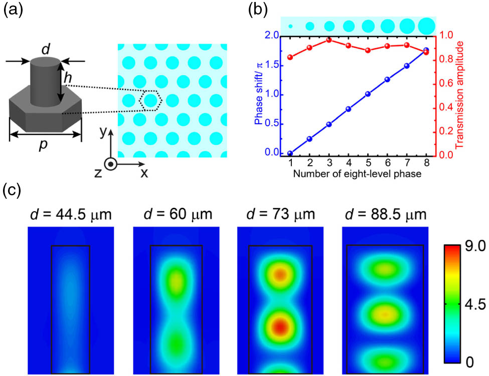
Figure 1.Schematic of the silicon pillar structure and the simulated results of the selected eight silicon pillars. (a) Schematic of a silicon pillar in the uniform hexagonal lattice on a silicon substrate. The lattice constant , and the pillar height . (b) Simulated phase shifts and transmission amplitudes of the eight selected silicon pillars with different diameters at 1.0 THz. The diameters corresponding to the pillars in the upper row from number 1–8 are , 44.5, 53.5, 60, 66.5, 73, 79.5, and 88.5 μm, respectively. (c) Simulated side views ( planes) of the magnetic energy density distributions in four silicon pillars among the eight selections with , 60, 73, and 88.5 μm, respectively, at 1.0 THz. An -polarized plane wave with magnetic energy density of 1 is normally incident on the silicon pillars from the bottom (substrate side).
3. RESULTS AND DISCUSSION
To verify the reliability of the eight-cylinder pillars experimentally, an anomalous deflector is first designed by arranging a linear abrupt phase profile. Figure 2(a) is a scanning electron microscope (SEM) image of part of the fabricated sample. A fiber-based angle-resolved terahertz time-domain spectroscopy (FAT TDS) system is utilized to characterize the sample under -polarized normal incidence, as schematically illustrated in Fig. 2(b). The generated terahertz wave is first collimated by a TPX lens L1, which then normally illuminates the deflector from the substrate side. Next, the output terahertz wave is focused on the receiver by a second TPX lens L2. The deflector is fixed at the center of a rotation stage. The receiver and the second lens are fixed on a rail mounted on the motorized rotator so as to collect the output terahertz waves that are deflected to different angles. During the measurement, the stage is gradually rotated from to 90° with a 1° step. The measured normalized far-field intensity distribution as a function of the deflection angle and the frequency is shown in Fig. 2(c). It is clearly seen that around the designed frequency of 1.0 THz, nearly all of the output wave is deflected to the desired angle. The corresponding normalized far-field intensity profile at 1.0 THz is extracted in Fig. 2(d). The deflection angle of the peak is 21.9°, which agrees well with the theoretical value calculated from the generalized Snell’s law, , with being the wavelength [3]. The integrated intensity of the peak is about 91.6% of the whole output. Though the deflector is designed at 1.0 THz, it exhibits a broadband feature across the whole observed range (0.5–1.5 THz), as illustrated in Fig. 2(c). The deflection angles at the first diffraction order are in good consistency with the theoretical calculation from the generalized Snell’s law. The intensity distributions at the other diffraction orders are due to the fact that the phase profiles at the other frequencies are no longer in good linear profile. Similar results could also be obtained under -polarized normal incidence.

Figure 2.SEM image and experimental results of the anomalous deflector. (a) SEM image of part of the anomalous deflector. Scale bar: 200 μm, same hereinafter. (b) Schematic of FAT TDS. (c) Measured normalized far-field intensity distribution as a function of the deflection angle and the frequency under normal incidence. (d) Corresponding far-field intensity profile at 1.0 THz extracted from (c).
Next, several metasurface Bessel and vortex beam generators are designed and experimentally characterized. Bessel beams can be applied in high-quality imaging, precision measurement, and optical alignment, owing to their diffraction-free and self-healing characteristics [42–44]. Vortex beams that carry orbital angular momentums have promising applications in high-dimensional communication systems and optical manipulation [45–48]. Conventionally, a 0th-order Bessel beam is realized by using an axicon lens or by filtering through a ring slit [42,43], and higher-order Bessel beams are generated by replenishing additional phase modulators [49]; vortex beams are generated by using spiral phase plates or holograms [50,51]. However, these conventional devices are either bulky or low efficient. To overcome such drawbacks, other methods that involve abrupt phase change have been proposed by applying mechanisms of Pancharatnam–Berry (PB) phase, effective waveguide effect, or resonance-induced phase shift through using inhomogeneous anisotropic media and metasurfaces [3,4,14,26,33,37,41,52–55]. Among them, dielectric metasurfaces provide a promising route to realize compact and efficient terahertz Bessel and vortex beam generators [33,37,41,54].
To generate an th-order Bessel beam using metasurfaces, the abrupt phase profile should be in both a spiral and a cone shape. The profile of the transmission coefficients is described by , where and represent the azimuthal angle and the radius in the polar coordinate, is the lattice vector, which is defined by the phase gradient in the radial direction, is the radial interval of phase difference [4,54]. Here, 0th-, first-, and second-order Bessel beam generators (B0, B1, and B2 generators, respectively) are designed and fabricated with . An SEM image of part of the B0 generator is illustrated in Fig. 3(a). The corresponding metasurfaces are characterized by using fiber-based near-field scanning terahertz microscopy (FNSTM), as illustrated in Fig. 3(b). The main difference between the FNSTM and FAT TDS characterizations is that, in FNSTM, the receiver is replaced by a 780 nm excited photoconductive-antenna-based terahertz near-field probe (Protemics GmbH) with a resolution up to 20 μm. In the detecting module, a fiber collimator, a periodically poled lithium niobate (PPLN) crystal, lenses L2 to L4, and a prism mirror, are used to double the 1560 nm centered fiber femto-second laser to 780 nm centered and then guide the laser to the probe. To enable a 2D scan of the terahertz electric field in the plane, the detecting module is mounted on a 2D translation stage. The sample is mounted on a 3D translation stage, which is used to adjust the position of the sample center in the direction and to enable a 3D field scan with an additional -direction adjustment. Figures 3(c), 3(f), and 3(i) illustrate the measured normalized intensity distributions in the planes, respectively, where non-diffracting propagation behaviors are clearly observed in a range longer than . Figures 3(d), 3(g), and 3(j) illustrate the corresponding measured normalized intensity distributions, while Figs. 3(e), 3(h), and 3(k) illustrate the corresponding measured phase distributions, in the planes at 5, 5, and 6 mm above the metasurfaces, respectively, showing good 0th-, first-, and second-order Bessel distributions. The hollow center of the higher-order Bessel beam is a result of the self-canceling effect induced by the spiral phase distribution. Meanwhile, the hollow center is larger in Bessel beams with a larger .
Figure 3.SEM image of the B0 generator and experimental results of the B0, B1, and B2 generators. (a) SEM image of part of the fabricated B0 generator. (b) Schematic of FNSTM. (c, f, i) Measured normalized intensity distributions of the B0, B1, and B2 generators in the planes, respectively, at 1.0 THz. (d, g, j) The corresponding measured normalized intensity distributions in the planes. (e, h, k) The corresponding measured phase distributions in the planes. The intensity and phase distributions in the planes of the B0, B1, and B2 generators are detected at 5, 5, and 6 mm away from the generators, respectively. The scanning step is 0.25 mm.
To generate an th-order vortex beam, the abrupt phase profile should be solely in a spiral shape. The profile of the transmission coefficients is described by , where represents the topological charge that determines the orbital angular momentum of the photon with being the Planck constant [55,56]. Here, first-, second-, and fourth-order terahertz vortex beam generators (V1, V2, and V4 generators, respectively) are designed and fabricated. The corresponding metasurfaces are equally divided into 8, 16, and 32 sections by their azimuthal angles. The eight selected silicon pillars are then arranged into these sections in sequence to form , , and spiral phase loops, respectively, in which each section consists of only one silicon pillar type. Figures 4(a), 4(d), and 4(g) illustrate the SEM images of part of the three metasurfaces, respectively. They are all characterized by using FNSTM. Figures 4(b), 4(e), and 4(h) show the measured phase distributions of the electric fields in the planes at a distance of 10 mm from the three metasurfaces at 1.0 THz, respectively. Three distinct orbital angular momentum states are clearly observed, as indicated by the one-, two-, and four-phase periods around the center of each respective metasurface. Figures 4(c), 4(f), and 4(i) illustrate the corresponding measured normalized intensity distributions, respectively, which are in good doughnut shapes. The hollow center is larger in vortex beams with a larger . This is also a direct consequence of the self-canceling effect induced by the spiral phase distribution.
Figure 4.SEM images and experimental results of the V1, V2, and V4 generators. (a, d, g) SEM images of part of the fabricated V1, V2, and V4 generators, respectively. The different color shades represent different phase sections schematically, as indicated by (a). (b, e, h) Measured phase distributions of the output electric fields of the V1, V2, and V4 generators, respectively, at 1.0 THz. (c, f, i) The corresponding measured normalized intensity distributions. All of the distributions are detected at a distance of 10 mm from the generators. The scanning step is 0.4 mm.
To investigate the efficiency of the proposed all-silicon dielectric metasurfaces, we carry out numerical simulations using CST Microwave Studio. Here, the efficiency is defined as the transmittance of just the interface with the silicon pillars, from the silicon substrate to the air. To imitate the real case, we set a Gaussian beam with a waist radius of 2000 μm at 1.0 THz in the simulation, which normally illuminates the metasurfaces from the substrate, across the silicon pillars, to the air. Then, the corresponding far-field amplitude distribution () is obtained by setting a field monitor. The same simulation is also carried out on bare silicon to obtain a reference far-field amplitude distribution (, inside the silicon). The efficiency is thus calculated as , where and are the integrated results of and , respectively. The efficiencies are 73.7% for the anomalous deflector, 82.5%, 74.7%, and 74.1% for the B0, B1, and B2 Bessel beam generators, and 81.5%, 76.6%, and 71.5% for the V1, V2, and V4 vortex beam generators, respectively. The corresponding measured efficiencies are 68.4% for the anomalous deflector; 78.9%, 72.3%, and 65.2% for the B0, B1, and B2 Bessel beam generators; and 75.2%, 73.4%, and 65.9% for the V1, V2, and V4 vortex beam generators, respectively. The measured efficiencies quite approach to the simulated results. The slight difference can be attributed to the fabrication derivations. In real applications, the efficiency will degrade due to an reflection loss at the back interface of the silicon substrate. This can be reduced by using substrates with a lower refractive index or by fabricating an antireflection coating on the back interface. For example, the antireflection coating can be silicon pillars, as shown in Fig. 1(a) with , , and . The simulated transmittance of such a metasurface at 1.0 THz can reach 99.5%.
One of the big advantages of the proposed dielectric metasurfaces is that they can be flexibly combined. Two arbitrary metasurfaces can be merged into one composite optical device, which can help realize controllable wavefront manipulation while retaining the compactness. Here, we take an experiment to show such ability. According to the required abrupt phase profiles of vortex and Bessel beam generators, an th-order Bessel beam can be obtained by combining an th-order vortex beam generator with an th-order Bessel beam generator. By sticking the V1 and B0 generators back to back, a composite first-order Bessel beam generator (CB1 generator) is obtained, as schematically illustrated in Fig. 5(a). The back interfaces are all identical polished-silicon surfaces, so the contact interface will not cause a reflection loss. Figure 5(b) illustrates the measured normalized intensity distribution in the plane, while Figs. 5(c) and 5(d) illustrate the corresponding measured normalized intensity and phase distributions in the plane at 5 mm away from the CB1 generator, respectively. Clear features of a first-order Bessel beam are observed, e.g., the size of the hollow center is similar to that of the first-order Bessel beam in Figs. 3(f) and 3(g), while smaller than that of the second-order Bessel beam in Figs. 3(i) and 3(j); the phase period in the azimuthal direction is . Such a property diversifies the functions of a certain group of metasurfaces.
Figure 5.Schematic of the CB1 generator and the corresponding experimental results. (a) Schematic of the CB1 composite beam generator composed of the V1 and B0 generators. The terahertz beam is incident from the V1 generator. (b) Measured normalized intensity distributions of the CB1 generator in the plane at 1.0 THz. (c, d) The corresponding measured normalized intensity and phase distributions in the plane, respectively. The intensity and phase distributions in the plane are detected at 5 mm away from the generator. The scanning step is 0.25 mm.
4. CONCLUSION
In conclusion, polarization-independent, terahertz, all-silicon dielectric metasurfaces consisting of cylindrical silicon pillars on a silicon substrate are presented. By varying the diameter of the pillars, whole range abrupt phase shift can be achieved so as to achieve nearly full control over the terahertz wavefront. Several typical terahertz devices are designed and experimentally characterized. The results all agree well with the theoretical prediction. A maximum efficiency of 82.5% can be achieved with our design. Furthermore, the metasurfaces can be easily combined to form composite devices that realize extended functions. Such dielectric metasurfaces are compatible with existing semiconductor technologies and are easy to fabricate, making them promising in developing next-generation low-loss and ultracompact terahertz functional devices.
References
[1] A. V. Kildishev, A. Boltasseva, V. M. Shalaev. Planar photonics with metasurfaces. Science, 339, 1232009(2013).
[2] N. Yu, F. Capasso. Flat optics with designer metasurfaces. Nat. Mater., 13, 139-150(2014).
[3] N. Yu, P. Genevet, M. A. Kats, F. Aieta, J. P. Tetienne, F. Capasso, Z. Gaburro. Light propagation with phase discontinuities: generalized laws of reflection and refraction. Science, 334, 333-337(2011).
[4] F. Aieta, P. Genevet, M. A. Kats, N. Yu, R. Blanchard, Z. Gahurro, F. Capasso. Aberration-free ultrathin flat lenses and axicons at telecom wavelengths based on plasmonic metasurfaces. Nano Lett., 12, 4932-4936(2012).
[5] X. Chen, L. Huang, H. Muhlenbernd, G. Li, B. Bai, Q. Tan, G. Jin, C. Qiu, S. Zhang, T. Zentgraf. Dual-polarity plasmonic metalens for visible light. Nat. Commun., 3, 1198(2012).
[6] N. Yu, F. Aieta, P. Genevet, M. A. Kats, Z. Gaburro, F. Capasso. A broadband, background-free quarter-Wave plate based on plasmonic metasurfaces. Nano Lett., 12, 6328-6333(2012).
[7] X. J. Ni, S. Ishii, A. V. Kildishev, V. M. Shalaev. Ultra-thin, planar, Babinet-inverted plasmonic metalenses. Light Sci. Appl., 2, e72(2013).
[8] X. J. Ni, A. V. Kildishev, V. M. Shalaev. Metasurface holograms for visible light. Nat. Commun., 4, 2807(2013).
[9] L. Huang, X. Chen, H. Muhlenbernd, H. Zhang, S. Chen, B. Bai, Q. Tan, G. Jin, K. W. Cheah, C. Qiu, J. S. Li, T. Zentgraf, S. Zhang. Three-dimensional optical holography using a plasmonic metasurface. Nat. Commun., 4, 2808(2013).
[10] X. Zhang, Z. Tian, W. Yue, J. Gu, S. Zhang, J. Han, W. Zhang. Broadband terahertz wave deflection based on C-shape complex metamaterials with phase discontinuities. Adv. Mater., 25, 4567-4572(2013).
[11] L. Liu, X. Zhang, M. Kenney, X. Su, N. Xu, C. Ouyang, Y. Shi, J. Han, W. Zhang, S. Zhang. Broadband metasurfaces with simultaneous control of phase and amplitude. Adv. Mater., 26, 5031-5036(2014).
[12] D. Hu, X. Wang, S. Feng, J. Ye, W. Sun, Q. Kan, P. J. Klar, Y. Zhang. Ultrathin terahertz planar elements. Adv. Opt. Mater., 1, 186-191(2013).
[13] Q. Wang, X. Zhang, Y. Xu, Z. Tian, J. Gu, W. Yue, S. Zhang, J. Han, W. Zhang. A broadband metasurface-based terahertz flat-lens array. Adv. Opt. Mater., 3, 779-785(2015).
[14] J. He, X. Wang, D. Hu, J. Ye, S. Feng, Q. Kan, Y. Zhang. Generation and evolution of the terahertz vortex beam. Opt. Express, 21, 20230-20239(2013).
[15] Q. Wang, X. Zhang, Y. Xu, J. Gu, Y. Li, Z. Tian, R. Singh, S. Zhang, J. Han, W. Zhang. Broadband metasurface holograms: toward complete phase and amplitude engineering. Sci. Rep., 6, 32867(2016).
[16] B. Wang, B. Quan, J. He, Z. Xie, X. Wang, J. Li, Q. Kan, Y. Zhang. Wavelength de-multiplexing metasurface hologram. Sci. Rep., 6, 35657(2016).
[17] X. Zhang, Y. Xu, W. Yue, Z. Tian, J. Gu, Y. Li, R. Singh, S. Zhang, J. Han, W. Zhang. Anomalous surface wave launching by handedness phase control. Adv. Mater., 27, 7123-7129(2015).
[18] F. Monticone, N. M. Estakhri, A. Alu. Full control of nanoscale optical transmission with a composite metascreen. Phys. Rev. Lett., 110, 203903(2013).
[19] A. Arbabi, A. Faraon. Fundamental limits of ultrathin metasurfaces. Sci. Rep., 7, 43722(2017).
[20] S. Sun, K. Yang, C. Wang, T. Juan, W. Chen, C. Liao, Q. He, S. Xiao, W. T. Kung, G. Guo, L. Zhou, D. Tsai. High-efficiency broadband anomalous reflection by gradient meta-surfaces. Nano Lett., 12, 6223-6229(2012).
[21] A. Pors, O. Albrektsen, I. P. Radko, S. I. Bozhevolnyi. Gap plasmon-based metasurfaces for total control of reflected light. Sci. Rep., 3, 2155(2013).
[22] C. Pfeiffer, A. Grbic. Metamaterial Huygens’ surfaces: tailoring wave fronts with reflectionless sheets. Phys. Rev. Lett., 110, 197401(2013).
[23] N. K. Grady, J. E. Heyes, D. R. Chowdhury, Y. Zeng, M. T. Reiten, A. K. Azad, A. J. Taylor, D. A. R. Dalvit, H. Chen. Terahertz metamaterials for linear polarization conversion and anomalous refraction. Science, 340, 1304-1307(2013).
[24] C. Pfeiffer, N. K. Emani, A. M. Shaltout, A. Boltasseva, V. M. Shalaev, A. Grbic. Efficient light bending with isotropic metamaterial Huygens’ surfaces. Nano Lett., 14, 2491-2497(2014).
[25] G. Zheng, H. Muhlenbernd, M. Kenney, G. Li, T. Zentgraf, S. Zhang. Metasurface holograms reaching 80% efficiency. Nat. Nanotechnol., 10, 308-312(2015).
[26] S. Liu, A. Noor, L. Du, L. Zhang, Q. Xu, K. Luan, T. Wang, Z. Tian, W. Tang, J. Han, W. Zhang, X. Zhou, Q. Cheng, T. Cui. Anomalous refraction and nondiffractive Bessel-beam generation of terahertz waves through transmission-type coding metasurfaces. ACS Photon., 3, 1968-1977(2016).
[27] S. Liu, Q. Cheng, Q. Xu, T. Wang, L. Du, K. Luan, Y. Xu, D. Bao, X. Fu, J. Han, W. Zhang, T. Cui. Free-standing metasurfaces for high-efficiency transmitarrays for controlling terahertz waves. Adv. Opt. Mater., 4, 384-390(2016).
[28] S. Jahani, Z. Jacob. All-dielectric metamaterials. Nat. Nanotechnol., 11, 23-36(2016).
[29] P. Genevet, F. Capasso, F. Aieta, M. Khorasaninejad, R. Devlin. Recent advances in planar optics: from plasmonic to dielectric metasurfaces. Optica, 4, 139-152(2017).
[30] S. Vo, D. Fattal, W. V. Sorin, Z. Peng, T. Tran, M. Fiorentino, R. G. Beausoleil. Sub-wavelength grating lenses with a twist. IEEE Photon. Tech. Lett., 26, 1375-1378(2014).
[31] D. Lin, P. Fan, E. Hasman, M. L. Brongersma. Dielectric gradient metasurface optical elements. Science, 345, 298-302(2014).
[32] M. Decker, I. Staude, M. Falkner, J. Dominguez, D. N. Neshev, I. Brener, T. Pertsch, Y. S. Kivshar. High-efficiency dielectric Huygens’ surfaces. Adv. Opt. Mater., 3, 813-820(2015).
[33] M. I. Shalaev, J. B. Sun, A. Tsukernik, A. Pandey, K. Nikolskiy, N. M. Litchinitser. High-efficiency all-dielectric metasurfaces for ultracompact beam manipulation in transmission mode. Nano Lett., 15, 6261-6266(2015).
[34] Y. F. Yu, A. Y. Zhu, R. Paniagua-Domínguez, Y. H. Fu, B. Luk’yanchuk, A. I. Kuznetsov. High-transmission dielectric metasurface with 2π phase control at visible wavelengths. Laser Photon. Rev., 9, 412-418(2015).
[35] M. Khorasaninejad, F. Capasso. Broadband multifunctional efficient meta-gratings based on dielectric waveguide phase shifters. Nano Lett., 15, 6709-6715(2015).
[36] A. Arbabi, Y. Horie, A. J. Ball, M. Bagheri, A. Faraon. A subwavelength-thick lenses with high numerical apertures and large efficiency based on high-contrast transmitarrays. Nat. Commun., 6, 7069(2015).
[37] A. Arbabi, Y. Horie, M. Bagheri, A. Faraon. Dielectric metasurfaces for complete control of phase and polarization with subwavelength spatial resolution and high transmission. Nat. Nanotechnol., 10, 937-943(2015).
[38] M. Khorasaninejad, A. Y. Zhu, C. Roques-Carmes, W. T. Chen, J. Oh, I. Mishra, R. C. Devlin, F. Capasso. Polarization-insensitive metalenses at visible wavelengths. Nano Lett., 16, 7229-7234(2016).
[39] Q.-T. Li, F. Dong, B. Wang, F. Gan, J. Chen, Z. Song, L. Xu, W. Chu, Y.-F. Xiao, Q. Gong, Y. Li. Polarization-independent and high-efficiency dielectric metasurfaces for visible light. Opt. Express, 24, 16309-16319(2016).
[40] D. Headland, E. Carrasco, S. Nirantar, W. Withayachumnankul, P. Gutruf, J. Schwarz, D. Abbott, M. Bhaskaran, S. Sriram, J. Perruisseau-Carrier, C. Fumeaux. Dielectric resonator reflectarray as high-efficiency nonuniform terahertz metasurface. ACS Photon., 3, 1019-1026(2016).
[41] Z. Ma, S. M. Hanham, P. Albella, B. H. Ng, H. T. Lu, Y. Gong, S. A. Maier, M. Hong. Terahertz all-dielectric magnetic mirror metasurfaces. ACS Photon., 3, 1010-1018(2016).
[42] J. Durnin, J. J. Miceli, J. H. Eberly. Diffraction-free beams. Phys. Rev. Lett., 58, 1499-1501(1987).
[43] Z. Bouchal, J. Wagner, M. Chlup. Self-reconstruction of a distorted nondiffracting beam. Opt. Commun., 151, 207-211(1998).
[44] E. Pastrana. Bessel beams beyond the limit. Nat. Methods, 10, 102-103(2013).
[45] D. G. Grier. A revolution in optical manipulation. Nature, 424, 810-816(2003).
[46] J. Wang, J. Yang, I. M. Fazal, N. Ahmed, Y. Yan, H. Huang, Y. Ren, Y. Yue, S. Dolinar, M. Tur, A. E. Willner. Terabit free-space data transmission employing orbital angular momentum multiplexing. Nat. Photonics, 6, 488-496(2012).
[47] A. E. Willner, J. Wang, H. Huang. A different angle on light communications. Science, 337, 655-656(2012).
[48] L. Yan, P. Gregg, E. Karimi, A. Rubano, L. Marrucci, R. Boyd, S. Ramachandran. Q-plate enabled spectrally diverse orbital-angular-momentum conversion for stimulated emission depletion microscopy. Optica, 2, 900-903(2015).
[49] J. Arlt, K. Dholakia. Generation of high-order Bessel beams by use of an axicon. Opt. Commun., 177, 297-301(2000).
[50] M. W. Beijersbergen, R. P. C. Coerwinkel, M. Kristensen, J. P. Woerdman. Helical-wavefront laser beams produced with a spiral phaseplate. Opt. Commun., 112, 321-327(1994).
[51] N. R. Heckenberg, R. McDuff, C. P. Smith, A. G. White. Generation of optical phase singularities by computer-generated holograms. Opt. Lett., 17, 221-223(1992).
[52] E. Karimi, S. A. Schulz, I. De Leon, H. Qassim, J. Upham, R. W. Boyd. Generating optical orbital angular momentum at visible wavelengths using a plasmonic metasurface. Light Sci. Appl., 3, e167(2014).
[53] F. Bouchard, I. De Leon, S. A. Schulz, J. Upham, E. Karimi, R. W. Boyd. Optical spin-to-orbital angular momentum conversion in ultra-thin metasurfaces with arbitrary topological charges. Appl. Phys. Lett., 105, 101905(2014).
[54] W. Chen, M. Khorasaninejad, A. Y. Zhu, J. Oh, R. C. Devlin, A. Zaidi, F. Capasso. Generation of wavelength-independent subwavelength Bessel beams using metasurfaces. Light Sci. Appl., 6, e16259(2017).
[55] L. Marrucci, C. Manzo, D. Paparo. Optical spin-to-orbital angular momentum conversion in inhomogeneous anisotropic media. Phys. Rev. Lett., 96, 163905(2006).
[56] L. Allen, M. W. Beijersbergen, R. J. C. Spreeuw, J. P. Woerdman. Orbital angular momentum of light and the transformation of Laguerre-Gaussian laser modes. Phys. Rev. A, 45, 8185-8189(1992).


