Contents
2020
Volume: 8 Issue 11
21 Article(s)

Export citation format
PEROVSKITE PHOTONICS
Phase segregation in inorganic mixed-halide perovskites: from phenomena to mechanisms
Yutao Wang, Xavier Quintana, Jiyun Kim, Xinwei Guan, Long Hu, Chun-Ho Lin, Brendon Tyler Jones, Weijian Chen, Xiaoming Wen, Hanwei Gao, and Tom Wu
Halide perovskites, such as methylammonium lead halide perovskites (MAPbX3, X=I, Br, and Cl), are emerging as promising candidates for a wide range of optoelectronic applications, including solar cells, light-emitting diodes, and photodetectors, due to their superior optoelectronic properties. All-inorganic lead halide perovskites CsPbX3 are attracting a lot of attention because replacing the organic cations with Cs+ enhances the stability, and its halide-mixing derivatives offer broad bandgap tunability covering nearly the entire visible spectrum. However, there is evidence suggesting that the optical properties of mixed-halide perovskites are influenced by phase segregation under external stimuli, especially illumination, which may negatively impact the performance of optoelectronic devices. It is reported that the mixed-halide perovskites in forms of thin films and nanocrystals are segregated into a low-bandgap I-rich phase and a high-bandgap Br-rich phase. Herein, we present a critical review on the synthesis and basic properties of all-inorganic perovskites, phase-segregation phenomena, plausible mechanisms, and methods to mitigate phase segregation, providing insights on advancing mixed-halide perovskite optoelectronics with reliable performance.
Photonics Research
  • Publication Date: Oct. 30, 2020
  • Vol. 8, Issue 11, A56 (2020)
Cavity engineering of two-dimensional perovskites and inherent light-matter interaction | On the Cover
Shuai Zhang, Yangguang Zhong, Fan Yang, Qinxuan Cao, Wenna Du, Jianwei Shi, and Xinfeng Liu
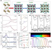
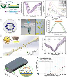
Two-dimensional (2D) perovskites are hybrid layered materials in which the inorganic lattice of an octahedron is sandwiched by organic layers. They behave as a quantum-well structure exhibiting large exciton binding energy and high emission efficiency, which is excellent for photonic applications. Hence, the cavity modulation and cavity devices of 2D perovskites are widely investigated. In this review, we summarize the rich photophysics, synthetic methods of different cavity structures, and the cavity-based applications of 2D perovskites. We highlight the strong exciton–photon coupling and photonic lasing obtained in different cavity structures. In addition, functional optoelectronic devices using cavity structures of 2D perovskites are also reviewed.
Photonics Research
  • Publication Date: Oct. 30, 2020
  • Vol. 8, Issue 11, A72 (2020)
TOPOLOGICAL PHOTONICS AND BEYOND
Manipulating light radiation from a topological perspective
Xuefan Yin, and Chao Peng
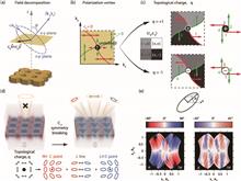
Manipulating radiation is important for a variety of optoelectronic applications, such as on-chip lasers, energy-efficient grating couplers, and antennas for light detection and ranging. Although designing and optimizing those optoelectronic devices are usually believed to be an engineering-oriented task, recent research reveals that the principles underlying radiation manipulation are closely connected to the concept of topology—the study of properties that are invariant under continuous deformations. In this review, we summarize a series of advances of the physics, phenomena, and applications related to radiation manipulation, in which topological concepts were adopted. Radiation could carry energy escaping from the system, breaking the energy conservation. The non-Hermiticity of such systems brings quite different physical consequences when comparing with the Hermitian counterparts and, hence, also results in the emergence of many interesting and extraordinary phenomena. In particular, it is found that the perfect trapping of light can still be realized in such non-Hermitian systems because of the photonic realization of bound states in the continuum. The fundamental nature of bound states in the continuum has been identified to be topological: they are essentially topological defects of the polarization vector field in momentum space, depicted by a kind of topological invariant named topological charges. Therefore, manipulation of radiation channels can be realized by controlling the topological charge evolution in momentum space. It is also demonstrated that the photonic states accompanied with different topological charges generate vortex beams with unique far-field radiation patterns, and ultra-fast switching of such vortex beams is demonstrated according to this principle. The progresses of topological photonics upon light radiation show that the topology is not just mathematical convenience for depicting photonic systems, but has brought realistic consequences in manipulating light and will boost the applications of photonics and optoelectronics in many aspects.
Photonics Research
  • Publication Date: Oct. 21, 2020
  • Vol. 8, Issue 11, B25 (2020)
Topologically protected long-range coherent energy transfer
Yujing Wang, Jun Ren, Weixuan Zhang, Lu He, and Xiangdong Zhang
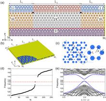
The realization of robust coherent energy transfer with a long range from a donor to an acceptor has many important applications in the field of quantum optics. However, it is hard to be realized using conventional schemes. Here, we demonstrate theoretically that robust energy transfer can be achieved using a photonic crystal platform, which includes the topologically protected edge state and zero-dimensional topological corner cavities. When the donor and the acceptor are put into a pair of separated topological cavities, the energy transfer between them can be fulfilled with the assistance of the topologically protected interface state. Such an energy transfer is robust against various kinds of defects, and can also occur over very long distances, which is very beneficial for biological detections, sensors, quantum information science, and so on.
Photonics Research
  • Publication Date: Oct. 30, 2020
  • Vol. 8, Issue 11, B39 (2020)
Reviews
Fiber Optics and Optical Communications
Micro- and nano-fiber probes for optical sensing, imaging, and stimulation in biomedical applications
Xia Yu, Shuyan Zhang, Malini Olivo, and Nanxi Li
The flexibile nature of optical fiber enables it to offer remote-access capabilities, which could be used in many biomedical applications. This review focuses on different micro- and nano-structured fiber probes for applications in biosensing, imaging, and stimulations. The modifications to fiber could extend design freedom from waveguide optimization to functional material integration. Fiber probes with optimized waveguide structures or integrated functional materials could achieve enhanced optical mode interaction with biosamples, and hence obtain ultrasensitive biosensors with a remarkably low limit of detection. Furthermore, bioimaging with a high spatial resolution can be obtained by engineering dispersion and nonlinearity of light propagation in the fiber core or designing a metal-coated tapered fiber tip with a sub-wavelength aperture. Flat metasurfaces can be assembled on a fiber tip to achieve a large depth of focus and remove aberrations. Fiber is also a compact solution to realize the precise delivery of light for in vivo applications, such as deep brain stimulation. The optical beam size, shape, and direction could be steered by the probe parameters. Micro- and nano-technologies integrated with fiber contribute to various approaches to further improve detection limit, sensitivity, optical resolution, imaging depth, and stimulation precision.
Photonics Research
  • Publication Date: Oct. 22, 2020
  • Vol. 8, Issue 11, 1703 (2020)
Optical Devices
Upconversion-luminescent hydrogel optical probe for in situ dopamine monitoring
Bingqian Zhou, Jingjing Guo, Changxi Yang, and Lingjie Kong
Dopamine (DA), as a neurotransmitter in human brain, plays a crucial role in reward motivation and motor control. An improper level of DA can be associated with neurological disorders such as schizophrenia and Parkinson’s disease. To quantify DA, optical DA sensors have emerged as an attractive platform due to their capability of high-precision and label-free measurement, and immunity to electromagnetic interference. However, the lack of selectivity, limited biocompatibility, and complex fabrication processes are challenges that hinder their clinical applications. Here, we report a soft and biocompatible luminescent hydrogel optical sensor capable of recognizing and quantifying DA with a simple and compact interrogation setup. The sensor is made of a hydrogel optical fiber (HOF) incorporated with upconversion nanoparticles (UCNPs). DA molecules are detected through the luminescence energy transfer (LET) between the UCNPs and the oxidation products of DA, while the light-guiding HOF enables both excitation and emission collection of the UCNPs. The hydrogel sensor provides an optical readout that shows a linear response up to 200 μmol/L with a detection limit as low as 83.6 nmol/L. Our results show that the UCNP-based hydrogel sensor holds great promise of serving as a soft and biocompatible probe for monitoring DA in situ.
Photonics Research
  • Publication Date: Oct. 30, 2020
  • Vol. 8, Issue 11, 1800 (2020)
Research Articles
Fiber Optics and Optical Communications
Dispersion-limited versus power-limited terahertz communication links using solid core subwavelength dielectric fibers
Kathirvel Nallappan, Yang Cao, Guofu Xu, Hichem Guerboukha, Chahé Nerguizian, and Maksim Skorobogatiy
Terahertz (THz) band (0.1–10 THz) is the next frontier for ultra-high-speed communication systems. Currently, most of communications research in this spectral range is focused on wireless systems, while waveguide/fiber-based links have been less explored. Although free space communications have several advantages such as convenience in mobility for the end user, as well as easier multi-device interconnectivity in simple environments, fiber-based communications provide superior performance in certain short-range communication applications such as multi-device connectivity in complex geometrical environments (ex., intra-vehicle connectivity) and secure communications with low probability of eavesdropping, as well as secure signal delivery to hard-to-reach or highly protected environments. In this work, we present an in-depth experimental and numerical study of the short-range THz communications links that use subwavelength dielectric fibers for information transmission and define the main challenges and trade-offs in the link implementation. Particularly, we use air or foam-cladded polypropylene-core subwavelength dielectric THz fibers of various diameters (0.57–1.75 mm) to study link performance as a function of the link length of up to ~10 m, and data bit rates of up to 6 Gbps at the carrier frequency of 128 GHz (2.34 mm wavelength). We find that depending on the fiber diameter, the quality of the transmitted signal is mostly limited either by the modal propagation loss or by the fiber velocity dispersion (GVD). An error-free transmission over 10 m is achieved for the bit rate of 4 Gbps using the fiber of smaller 0.57 mm diameter. Furthermore, since the fields of subwavelength fibers are weakly confined and extend deep into the air cladding, we study the modal field extent outside of the fiber core, as well as fiber bending loss. Finally, the power budget of the rod-in-air subwavelength THz fiber-based links is compared to that of free space communication links, and we demonstrate that fiber links offer an excellent solution for various short-range applications.
Photonics Research
  • Publication Date: Oct. 22, 2020
  • Vol. 8, Issue 11, 1757 (2020)
Imaging Systems, Microscopy, and Displays
High-speed dual-view band-limited illumination profilometry using temporally interlaced acquisition
Cheng Jiang, Patrick Kilcullen, Yingming Lai, Tsuneyuki Ozaki, and Jinyang Liang
We report dual-view band-limited illumination profilometry (BLIP) with temporally interlaced acquisition (TIA) for high-speed, three-dimensional (3D) imaging. Band-limited illumination based on a digital micromirror device enables sinusoidal fringe projection at up to 4.8 kHz. The fringe patterns are captured alternately by two high-speed cameras. A new algorithm, which robustly matches pixels in acquired images, recovers the object’s 3D shape. The resultant TIA–BLIP system enables 3D imaging over 1000 frames per second on a field of view (FOV) of up to 180 mm × 130 mm (corresponding to 1180×860 pixels) in captured images. We demonstrated TIA–BLIP’s performance by imaging various static and fast-moving 3D objects. TIA–BLIP was applied to imaging glass vibration induced by sound and glass breakage by a hammer. Compared to existing methods in multiview phase-shifting fringe projection profilometry, TIA–BLIP eliminates information redundancy in data acquisition, which improves the 3D imaging speed and the FOV. We envision TIA–BLIP to be broadly implemented in diverse scientific studies and industrial applications.
Photonics Research
  • Publication Date: Oct. 30, 2020
  • Vol. 8, Issue 11, 1808 (2020)
Lasers and Laser Optics
Generation of multi-channel chaotic signals with time delay signature concealment and ultrafast photonic decision making based on a globally-coupled semiconductor laser network
Yanan Han, Shuiying Xiang, Yang Wang, Yuanting Ma, Bo Wang, Aijun Wen, and Yue Hao
We propose and demonstrate experimentally and numerically a network of three globally coupled semiconductor lasers (SLs) that generate triple-channel chaotic signals with time delayed signature (TDS) concealment. The effects of the coupling strength and bias current on the concealment of the TDS are investigated. The generated chaotic signals are further applied to reinforcement learning, and a parallel scheme is proposed to solve the multiarmed bandit (MAB) problem. The influences of mutual correlation between signals from different channels, the sampling interval of signals, and the TDS concealment on the performance of decision making are analyzed. Comparisons between the proposed scheme and two existing schemes show that, with a simplified algorithm, the proposed scheme can perform as well as the previous schemes or even better. Moreover, we also consider the robustness of decision making performance against a dynamically changing environment and verify the scalability for MAB problems with different sizes. This proposed globally coupled SL network for a multi-channel chaotic source is simple in structure and easy to implement. The attempt to solve the MAB problem in parallel can provide potential values in the realm of the application of ultrafast photonics intelligence.
Photonics Research
  • Publication Date: Oct. 30, 2020
  • Vol. 8, Issue 11, 1792 (2020)
Nanophotonics and Photonic Crystals
Freestanding metal nanohole array for high-performance applications
Bobo Du, Yinlan Ruan, Dexing Yang, Peipei Jia, Shoufei Gao, Yingying Wang, Pu Wang, and Heike Ebendorff-Heidepriem
Plasmonic devices using periodic metallic nanostructures have recently gained tremendous interest for color filters, sensing, surface enhanced spectroscopy, and enhanced photoluminescence, etc. However, the performance of such plasmonic devices is severely hampered by the solid substrates supporting the metallic nanostructures. Here, a strategy for freestanding metallic nanomembranes is introduced by taking advantages of hollow substrate structures. Large-area and highly uniform gold nanomembranes with nanohole array are fabricated via a flexible and simple replication-releasing method. The hollow structures include a hollow core fiber with 30 μm core diameter and two ferrules with their hole diameter as 125 and 500 μm, respectively. As a proof-of-concept demonstration, 2 times higher sensitivity of the bulk refractive index is obtained with this platform compared to that of a counterpart on a solid silica substrate. Such a portable and compact configuration provides unique opportunities to explore the intrinsic properties of the metal nanomembranes and paves a new way to fabricate high-performance plasmonic devices for biomolecule sensing and color filter.
Photonics Research
  • Publication Date: Oct. 22, 2020
  • Vol. 8, Issue 11, 1749 (2020)
Nonlinear Optics
Revealing the intrinsic nonlinear optical response of a single MoS2 nanosheet in a suspension based on spatial self-phase modulation
Si Xiao, Ying Ma, Yilin He, Yiduo Wang, Hao Xin, Qi Fan, Jingdi Zhang, Xiaohong Li, Yu Zhang, Jun He, and Yingwei Wang
The reorientation of 2D materials caused by nonlocal electron coherence is the formation mechanism of 2D material spatial self-phase modulation under laser irradiation, which is widely known as the “wind-chime” model. Here, we present a method that provides strong evidence for the reorientation of 2D-material-induced spatial self-phase modulation. The traditional “wind-chime” model was modified by taking into account the attenuation, i.e., damping of the incident light beam in the direction of the optical path. Accordingly, we can extract the nonlinear refractive index of a single MoS2 nanosheet, instead of simply obtaining the index from an equivalent MoS2 film that was constructed by all nanosheets. Our approach introduces a universal and accurate method to extract intrinsic nonlinear optical parameters from 2D material systems.
Photonics Research
  • Publication Date: Oct. 22, 2020
  • Vol. 8, Issue 11, 1725 (2020)
Nanowire-assisted microcavity in a photonic crystal waveguide and the enabled high-efficiency optical frequency conversions
Linpeng Gu, Liang Fang, Qingchen Yuan, Xuetao Gan, Hao Yang, Xutao Zhang, Juntao Li, Hanlin Fang, Vladislav Khayrudinov, Harri Lipsanen, Zhipei Sun, and Jianlin Zhao
We report an indium phosphide nanowire (NW)-induced cavity in a silicon planar photonic crystal (PPC) waveguide to improve the light–NW coupling. The integration of NW shifts the transmission band of the PPC waveguide into the mode gap of the bare waveguide, which gives rise to a microcavity located on the NW section. Resonant modes with Q factors exceeding 103 are obtained. Leveraging on the high density of the electric field in the microcavity, the light–NW interaction is enhanced strongly for efficient nonlinear frequency conversion. Second-harmonic generation and sum-frequency generation in the NW are realized with a continuous-wave pump laser in a power level of tens of microwatts, showing a cavity-enhancement factor of 112. The hybrid integration structure of NW-PPC waveguide and the self-formed microcavity not only opens a simple strategy to effectively enhance light–NW interactions, but also provides a compact platform to construct NW-based on-chip active devices.
Photonics Research
  • Publication Date: Oct. 22, 2020
  • Vol. 8, Issue 11, 1734 (2020)
Optical and Photonic Materials
Two-dimensional tin diselenide nanosheets pretreated with an alkaloid for near- and mid-infrared ultrafast photonics
Zhenhong Wang, Bin Zhang, Bing Hu, Zhongjun Li, Chunyang Ma, Yu Chen, Yufeng Song, Han Zhang, Jun Liu, and Guohui Nie
Two-dimensional (2D) tin diselenide (SnSe2), a novel layered material with excellent optical and electronic properties, has been extensively investigated in various promising applications, including photodetectors, optical switching, and ultrafast photonics. In this work, SnSe2 nanosheets have been obtained after pretreatment in an alkaloid, exhibiting high optical absorption and electron-enriched properties. Besides, the performances of the prepared SnSe2 in near-infrared (NIR) and mid-infrared (MIR) ultrafast photonics are presented. Notably, by employing the SnSe2-deposited microfiber device as a saturable absorber (SA) exhibiting typical nonlinear optical absorption properties, stable ultrashort pulses and rogue waves are realized in an erbium-doped fiber laser. Furthermore, the SnSe2-deposited SA device is also applied to a thulium-doped fiber laser to achieve stable ultrashort pulses. This study indicates that SnSe2 is expected to be a suitable candidate for ultrafast fiber lasers in the NIR and MIR regions.
Photonics Research
  • Publication Date: Oct. 12, 2020
  • Vol. 8, Issue 11, 1687 (2020)
Optical Devices
Universal frequency engineering tool for microcavity nonlinear optics: multiple selective mode splitting of whispering-gallery resonances
Xiyuan Lu, Ashutosh Rao, Gregory Moille, Daron A. Westly, and Kartik Srinivasan
Whispering-gallery microcavities have been used to realize a variety of efficient parametric nonlinear optical processes through the enhanced light–matter interaction brought about by supporting multiple high quality factor and small modal volume resonances. Critical to such studies is the ability to control the relative frequencies of the cavity modes, so that frequency matching is achieved to satisfy energy conservation. Typically this is done by tailoring the resonator cross section. Doing so modifies the frequencies of all of the cavity modes, that is, the global dispersion profile, which may be undesired, for example, in introducing competing nonlinear processes. Here, we demonstrate a frequency engineering tool, termed multiple selective mode splitting (MSMS), that is independent of the global dispersion and instead allows targeted and independent control of the frequencies of multiple cavity modes. In particular, we show controllable frequency shifts up to 0.8 nm, independent control of the splitting of up to five cavity modes with optical quality factors ?105, and strongly suppressed frequency shifts for untargeted modes. The MSMS technique can be broadly applied to a wide variety of nonlinear optical processes across different material platforms and can be used to both selectively enhance processes of interest and suppress competing unwanted processes.
Photonics Research
  • Publication Date: Oct. 12, 2020
  • Vol. 8, Issue 11, 1676 (2020)
Optoelectronics
Efficient emission of InGaN-based light-emitting diodes: toward orange and red | Editors' Pick
Shengnan Zhang, Jianli Zhang, Jiangdong Gao, Xiaolan Wang, Changda Zheng, Meng Zhang, Xiaoming Wu, Longquan Xu, Jie Ding, Zhijue Quan, and Fengyi Jiang
Indium gallium nitride (InGaN)-based light-emitting diodes (LEDs) are considered a promising candidate for red-green-blue (RGB) micro displays. Currently, the blue and green LEDs are efficient, while the red ones are inefficient for such applications. This paper reports our work of creating efficient InGaN-based orange and red LEDs on silicon(111) substrates at low current density. Based on the structure of InGaN yellow LEDs, by simply reducing the growth temperature of all the yellow quantum wells (QWs), we obtained 599 nm orange LEDs with peak wall-plug efficiency (WPE) of 18.1% at 2 A/cm2. An optimized QW structure was proposed that changed two of the nine yellow QWs to orange ones. Compared with the sample containing nine orange QWs, the sample with two orange QWs and seven yellow QWs showed similar emission spectra but a much higher peak WPE up to 24.0% at 0.8 A/cm2 with a wavelength of 608 nm. The improvement of peak WPE can be attributed to the improved QW quality and the reduced active recombination volume. Subsequently, a series of efficient InGaN-based orange and red LEDs was demonstrated. With further development, the InGaN-based red LEDs are believed to be attainable and can be used in micro LED displays.
Photonics Research
  • Publication Date: Oct. 09, 2020
  • Vol. 8, Issue 11, 1671 (2020)
Modeling the degradation mechanisms of AlGaN-based UV-C LEDs: from injection efficiency to mid-gap state generation
F. Piva, C. De Santi, M. Deki, M. Kushimoto, H. Amano, H. Tomozawa, N. Shibata, G. Meneghesso, E. Zanoni, and M. Meneghini
In this work, we analyze and model the effect of a constant current stress on an ultraviolet light-emitting diode with a nominal wavelength of 285 nm. By carrying out electrical, optical, spectral, and steady-state photocapacitance (SSPC) analysis during stress, we demonstrate the presence of two different degradation mechanisms. The first one occurs in the first 1000 min of stress, is ascribed to the decrease in the injection efficiency, and is modeled by considering the defect generation dynamics related to the de-hydrogenation of gallium vacancies, according to a system of three differential equations; the second one occurs after 1000 min of stress and is correlated with the generation of mid-gap defects, for which we have found evidence in the SSPC measurements. Specifically, we detected the presence of deep-level states (at 1.6 eV) and mid-gap states (at 2.15 eV), indicating that stress induces the generation of non-radiative recombination centers.
Photonics Research
  • Publication Date: Oct. 30, 2020
  • Vol. 8, Issue 11, 1786 (2020)
Quantum Optics
Reducing the mode-mismatch noises in atom–light interactions via optimization of the temporal waveform
Xiaotian Feng, Zhifei Yu, Bing Chen, Shuying Chen, Yuan Wu, Donghui Fan, Chun-Hua Yuan, L. Q. Chen, Z. Y. Ou, and Weiping Zhang
Atom–light interface is at the core of quantum metrology and quantum information science. Associated noises during interaction processes are always inevitable and adverse. In this paper, we perform the stimulated Raman scattering (SRS) in a hot Rb87 vapor cell and demonstrate the reduction of related noises originated from mode mismatch via optimizing the temporal waveform of the input seed. By using the seed with the optimized mode, the intensity fluctuation of the signal field generated in atom–light interaction is decreased by 4.3 dB. Furthermore, the fluctuation of the intensity difference between the signal and atomic spin wave is reduced by 3.1 dB. Such a temporal mode-cleaning method can be applied to improve the precision of atom interferometry using SRS and should be helpful for quantum information processing based on an atom–light correlated system.
Photonics Research
  • Publication Date: Oct. 14, 2020
  • Vol. 8, Issue 11, 1697 (2020)
Silicon Photonics
Hybrid nano-scale Au with ITO structure for a high-performance near-infrared silicon-based photodetector with ultralow dark current
Xinxin Li, Zhen Deng, Jun Li, Yangfeng Li, Linbao Guo, Yang Jiang, Ziguang Ma, Lu Wang, Chunhua Du, Ying Wang, Qingbo Meng, Haiqiang Jia, Wenxin Wang, Wuming Liu, and Hong Chen
An internal photoemission-based silicon photodetector detects light below the silicon bandgap at room temperature and can exhibit spectrally broad behavior, making it potentially suited to meet the need for a near-infrared pure Si photodetector. In this work, the implementation of a thin Au insertion layer into an ITO/n-Si Schottky photodetector can profoundly affect the barrier height and significantly improve the device performance. By fabricating a nanoscale thin Au layer and an ITO electrode on a silicon substrate, we achieve a well-behaved ITO/Au/n-Si Schottky diode with a record dark current density of 3.7×10⁻⁷ A/cm2 at -1 V and a high rectification ratio of 1.5×10⁸ at ±1 V. Furthermore, the responsivity has been obviously improved without sacrificing the dark current performance of the device by decreasing the Au thickness. Such a silicon-based photodetector with an enhanced performance could be a promising strategy for the realization of a monolithic integrated pure silicon photodetector in optical communication.
Photonics Research
  • Publication Date: Oct. 09, 2020
  • Vol. 8, Issue 11, 1662 (2020)
800 Gbit/s transmission over 1 km single-mode fiber using a four-channel silicon photonic transmitter | Editors' Pick
Hongguang Zhang, Miaofeng Li, Yuguang Zhang, Di Zhang, Qiwen Liao, Jian He, Shenglei Hu, Bo Zhang, Lei Wang, Xi Xiao, Nan Qi, and Shaohua Yu
We demonstrate the optical transmission of an 800 Gbit/s (4×200 Gbit/s) pulse amplitude modulation-4 (PAM-4) signal and a 480 Gbit/s (4×120 Gbit/s) on–off-keying (OOK) signal by using a high-bandwidth (BW) silicon photonic (SiP) transmitter with the aid of digital signal processing (DSP). In this transmitter, a four-channel SiP modulator chip is co-packaged with a four-channel driver chip, with a measured 3 dB BW of 40 GHz. DSP is applied in both the transmitter and receiver sides for pre-/post-compensation and bit error rate (BER) calculation. Back-to-back (B2B) BERs of the PAM-4 signal and OOK signal are first measured for each channel of the transmitter with respect to a variety of data rates. Similar BER performance of four channels shows good uniformity of the transmitter between different channels. The BER penalty of the PAM-4 and OOK signals for 500 m and 1 km standard single-mode fiber (SSMF) transmission is then experimentally tested by using one channel of the transmitter. For a 200 Gbit/s PAM-4 signal, the BER is below the hard-decision forward error correction (HD-FEC) threshold for B2B and below the soft-decision FEC (SD-FEC) threshold after 1 km transmission. For a 120 Gbit/s OOK signal, the BER is below SD-FEC threshold for B2B. After 500 m and 1 km transmission, the data rate of the OOK signal shrinks to 119 Gbit/s and 118 Gbit/s with the SD-FEC threshold, respectively. Finally, the 800 Gbit/s PAM-4 signal with 1 km transmission is achieved with the BER of all four channels below the SD-FEC threshold.
Photonics Research
  • Publication Date: Oct. 26, 2020
  • Vol. 8, Issue 11, 1776 (2020)
Surface Optics and Plasmonics
All-metallic metasurfaces towards high-performance magneto-plasmonic sensing devices
Lixia Li, Xueyang Zong, and Yufang Liu
Magneto-plasmonic sensors based on surface plasmon resonance have been studied considerably in recent years, as they feature high sensitivity and ultrahigh resolution. However, the majority of such investigations focus on prism-based sandwich architectures that not only impede the miniaturization of devices but also have a weak transverse magneto-optical Kerr effect (TMOKE) in magnitude. Herein, we theoretically demonstrate a magneto-plasmonic sensor composed of Au/Co bilayer nanodisk arrays on top of optically thick metallic films, which supports a narrow surface plasmon resonance (SPR) with a bandwidth of 7 nm and allows for refractive index sensitivities as high as 717 nm/RIU. Thanks to the high-quality SPR mode, a Fano-like TMOKE spectrum with a subnanometer bandwidth can be achieved in the proposed structure, thereby giving rise to ultrahigh sensing of merit values as large as 7000 in water. Moreover, we demonstrate a large TMOKE magnitude that exceeds 0.6. The value is 1 order of magnitude larger than that of magneto-plasmonic sensors reported. We also demonstrate that the behavior of TMOKE spectra can be controlled by tuning the geometrical parameters of the device including the diameter and thickness of nanodisk arrays. This work provides a promising route for designing magneto-plasmonic sensors based on metasurfaces or metamaterials.
Photonics Research
  • Publication Date: Oct. 22, 2020
  • Vol. 8, Issue 11, 1742 (2020)
Comments
Comments
Coupled quantum molecular cavity optomechanics with surface plasmon enhancement: comment
Seyed Mahmoud Ashrafi, Narjes Taghadomi, Alireza Bahrampour, and Rasoul Malekfar
We have found an incorrect formula to estimate the root mean square (rms) amplitude of the molecular vibration in the molecular optomechanics systems reported by J. Liu et al. [Photon. Res.5, 450–456 (2017)PRHEIZ2327-912510.1364/PRJ.5.000450]. In contrast with common optomechanical systems, the equilibrium position for molecular optomechanics systems used in the letter cannot be achieved by the equipartition theorem. Here, we achieve the effective temperature of molecules and then provide a corrected formula for the estimation of the rms amplitude of molecular motion. Using defined effective temperature into our new formula, we show that the minimal measurable force is (F≈1.7×10⁻¹⁴ N), which it is 1 order bigger than the result of the main paper, and it is also in accordance with numerical calculation through the Lindblad master equation.
Photonics Research
  • Publication Date: Oct. 26, 2020
  • Vol. 8, Issue 11, 1783 (2020)