• Photonics Research
  • Vol. 8, Issue 11, 1776 (2020)
Hongguang Zhang1、†, Miaofeng Li1、2、†, Yuguang Zhang1、2, Di Zhang3, Qiwen Liao4、5, Jian He4、5, Shenglei Hu1, Bo Zhang3, Lei Wang1、2, Xi Xiao1、2、6、*, Nan Qi4、5、7、*, and Shaohua Yu1、2
Author Affiliations
  • 1National Information Optoelectronics Innovation Center, China Information and Communication Technologies Group Corporation (CICT), Wuhan 430074, China
  • 2State Key Laboratory of Optical Communication Technologies and Networks, China Information and Communication Technologies Group Corporation (CICT), Wuhan 430074, China
  • 3Accelink Technologies Co., Ltd., Wuhan 430205, China
  • 4State Key Laboratory of Superlattices and Microstructures, Institute of Semiconductors, Chinese Academy of Sciences, Beijing 100083, China
  • 5Center of Material Science and Optoelectronics Engineering, University of Chinese Academy of Sciences, Beijing 100049, China
  • 6e-mail: xxiao@wri.com.cn
  • 7e-mail: qinan@semi.ac.cn
  • show less
    DOI: 10.1364/PRJ.396815 Cite this Article Set citation alerts
    Hongguang Zhang, Miaofeng Li, Yuguang Zhang, Di Zhang, Qiwen Liao, Jian He, Shenglei Hu, Bo Zhang, Lei Wang, Xi Xiao, Nan Qi, Shaohua Yu. 800 Gbit/s transmission over 1 km single-mode fiber using a four-channel silicon photonic transmitter[J]. Photonics Research, 2020, 8(11): 1776 Copy Citation Text show less

    Abstract

    We demonstrate the optical transmission of an 800 Gbit/s (4×200 Gbit/s) pulse amplitude modulation-4 (PAM-4) signal and a 480 Gbit/s (4×120 Gbit/s) on–off-keying (OOK) signal by using a high-bandwidth (BW) silicon photonic (SiP) transmitter with the aid of digital signal processing (DSP). In this transmitter, a four-channel SiP modulator chip is co-packaged with a four-channel driver chip, with a measured 3 dB BW of 40 GHz. DSP is applied in both the transmitter and receiver sides for pre-/post-compensation and bit error rate (BER) calculation. Back-to-back (B2B) BERs of the PAM-4 signal and OOK signal are first measured for each channel of the transmitter with respect to a variety of data rates. Similar BER performance of four channels shows good uniformity of the transmitter between different channels. The BER penalty of the PAM-4 and OOK signals for 500 m and 1 km standard single-mode fiber (SSMF) transmission is then experimentally tested by using one channel of the transmitter. For a 200 Gbit/s PAM-4 signal, the BER is below the hard-decision forward error correction (HD-FEC) threshold for B2B and below the soft-decision FEC (SD-FEC) threshold after 1 km transmission. For a 120 Gbit/s OOK signal, the BER is below SD-FEC threshold for B2B. After 500 m and 1 km transmission, the data rate of the OOK signal shrinks to 119 Gbit/s and 118 Gbit/s with the SD-FEC threshold, respectively. Finally, the 800 Gbit/s PAM-4 signal with 1 km transmission is achieved with the BER of all four channels below the SD-FEC threshold.

    1. INTRODUCTION

    With the ever-increasing demand for high-speed intra- and inter-data-center connections, optical transceivers with lane rates of 100 Gbit/s are standardized in IEEE Standard 802.3bs [1]. The volume shipments of 400 GbE interconnect devices are expected to be dominant by 2020–2021 [2]. For the next generation of data center networks (DCNs) and data center interconnections (DCIs), an 800 GE interface (i.e., four-lane 200 Gbit/s per wavelength) is potentially a competitive solution that attracts more and more attention. To realize a 200 Gbit/s per wavelength interface, simple non-return to zero-on–off-keying (NRZ-OOK) signal format may no longer be sufficient to support the speed requirements [3], because the expected bandwidth (BW) for a transmitter (TX) and receiver (RX) is more than 100 GHz [4], which could be a terrible challenge for commercial production. Advanced modulation formats, such as discrete multi-tone (DMT), carrier-less amplitude phase (CAP), or multi-level pulse amplitude modulation (PAM), which allow for increased capacity at constant BW, are considered as potential solutions and have been widely researched [3]. PAM-4, as the simplest high-order modulation format, shows the lowest optical power penalty for single-laser 100G short-reach DCI links [5]. In IEEE Standard 802.3bs, PAM-4 with intensity modulation and direct detection (IM-DD) is standardized as one of the solutions for 400GbE interface (e.g., 400G-DR4). When updating lane rate from 100 Gbit/s to 200 Gbit/s per wavelength, the PAM-4 format is probably much inherited from the 400GE standard. Recently, many research experiments about 200 Gbit/s per wavelength transmission based on PAM-4 modulation have been reported for short-reach transmission using modulators with different kinds of materials, such as a LiNbO3 Mach–Zehnder modulator (MZM) [6,7], a lithium niobate on insulator (LNOI) modulator [8], a distributed feedback laser monolithically integrated with an MZM (DFB-MZM) [9], and an electlro-absorption modulated laser (EML) [1012]. In addition to LiNbO3 and indium phosphide (InP), silicon photonics (SiP) is also regarded as a high-potential platform for volume production of commercial optoelectronic devices. SiP technology has already been applied in commercial 100GbE interconnect devices [2], and it is expected to address next-generation optical interconnect due to its small footprint, low power, and complementary metal-oxide-semiconductor (CMOS) compatibility. High-speed transmission using SiP has also been extensively researched [1315].

    The works just listed focus on single-channel high-speed transmission. For the silicon platform, monolithic integration, which means complex and/or multi-channel functions are fabricated on the same photonic integrated circuit (PIC) chip, is also an important metric for commercial application [16]. Co-packaging and co-design of SiP modulators with RF integrated circuit (RFIC) drivers is a compelling technology to realize energy-efficient, high-BW optical interconnections [17]. A SiP transmitter integrated with a laser and/or driver is demonstrated in Refs. [1820] for 100 Gbit/s per wavelength PAM-4 transmission. In Ref. [21], four-channel 100 Gbaud PAM-4 transmission is demonstrated with the aid of digital signal processing (DSP); however, the experiment is based on discrete drivers and MZMs but not an integrated silicon device.

    In this paper, a four-channel SiP MZM chip is integrated with a four-channel driver chip by chip-on-board co-packaging, and a high-speed four-channel SiP transmitter is fabricated. 800 Gbit/s PAM-4 signal transmission and 480 Gbit/s OOK signal transmission using the co-packaged four-channel SiP transmitter are experimentally demonstrated for the first time, to the best of our knowledge. Offline DSP is applied both in the TX side and RX side as pre- and post-compensation to deal with BW limitation and chromatic dispersion (CD) penalty. Different baud rates of PAM-4 signal and OOK signal are modulated on each channel of the transmitter, and the B2B BER is measured to study the uniformity of different channels. Transmission penalty of the PAM-4 and OOK signals for 500 m and 1 km SSMF is then experimentally tested by using one channel of the transmitter, which shows that a 200 Gbit/s PAM-4 signal could achieve 1 km SSMF transmission with the BER lower than the SD-FEC threshold. For the OOK signal, after 500 m and 1 km SSMF transmission, the data rate shrinks to 119 Gbit/s and 118 Gbit/s with SD-FEC threshold. The 800 Gbit/s PAM-4 signal with 1 km transmission is tested, and the BER of each channel is below the SD-FEC threshold.

    2. SiP TRANSMITTER DESIGN AND FABRICATION

    Figure 1(a) shows a micrograph of the SiP MZM transmitter on the evaluation printed circuit board (PCB), which integrates a four-channel SiP MZM chip and a four-channel driver chip. The four-channel driver and the SiP MZM chip are DC coupled to simplify the packaging. The channel-to-channel distance is set to be 625 μm to prevent inter-channel electrical cross talk. Two input edge couplers are used for optical source input to the quad-modulators (i.e., each input is divided into two MZMs) with a comprehensive trade-off of output optical power and transmitter power consumption. Four optical output edge couplers with deep trenches to eliminate optical cross talk are used to couple output signals independently with a four-channel fiber array (FA).

    (a) Micrograph of the chip-on-board SiP transmitter that co-packaged a four-channel MZM chip and a four-channel driver by wire bonding on the evaluation board, (b) micrograph of the travelling wave electrode, and (c) schematic diagram of the active waveguide’s cross section.

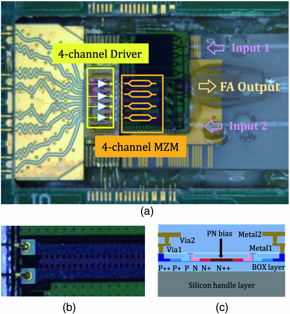
    Figure 1.(a) Micrograph of the chip-on-board SiP transmitter that co-packaged a four-channel MZM chip and a four-channel driver by wire bonding on the evaluation board, (b) micrograph of the travelling wave electrode, and (c) schematic diagram of the active waveguide’s cross section.

    The design and fabrication process of the SiP MZM are improved from our previous work [22], in which 90 Gbaud NRZ-OOK modulation was experimentally demonstrated. The four-channel SiP MZM modulators are fabricated at a commercial foundry on a high-resistivity silicon-on-insulator (SOI) wafer with a 220 nm-thick silicon layer, a 3 μm-thick buried oxide (BOX), a 700 μm silicon substrate layer, and a 90 nm-thick slab. To achieve higher BW and higher extinction ratio, a differential-driven travelling wave (TW) electrode design with T-shape rail formation is utilized, as shown in Fig. 1(b). As described in Ref. [23], perfect refractive index matching can be achieved at a specific P-N junction loaded electrode impedance. Figure 1(c) displays the cross-sectional structure of the active waveguide of the MZM. Two series of depletion-type P-N junctions are connected in push–pull mode. The P-N junctions are implemented by six implantation processes, with the doping concentration in the central waveguide to be 5×10¹⁷  cm3. The doping density at the slab silicon is optimized to reduce the active region’s resistance while keeping a lower optical loss. A DC bias voltage is applied to the N++ slab to reverse bias the P-N junctions. The modulator is biased at the quadrature point by tuning a thermal optical phase shifter with the TiN heater. The electro-optic (EO) BW of four-channel SiP modulator is measured to be 60 GHz, as shown in Fig. 2(a).

    EO S21 of the (a) SiP modulator and (b) SiP transmitter co-packaged with the driver.

    Figure 2.EO S21 of the (a) SiP modulator and (b) SiP transmitter co-packaged with the driver.

    The four-channel SiGe driver is co-designed with the SiP MZM chip, according to the modulator’s circuit model. To enable more than 100 Gbaud per-lane transmission, the driver is well designed to achieve high BW with our experience in EO co-design [24,25]. To optimize the overall BW and power consumption of the SiP transmitter, both the driver’s output impedance and the MZM’s characteristic impedance are optimized to 65Ω. In each lane of the driver, there is a multi-stage input buffer and output stage [2428]. The buffer has efficient equalization (EQ) ability utilizing resistor–capacitor (RC) degeneration to compensate for PCB trace losses and to optimize the integrated BW of the SiP transmitter after packaging [26]. A variant gain amplifier (VGA) is implemented to provide 10 dB tuning range. Because BW and linearity are dominant design challenges in a high-swing PAM-4 driver, several BW extension techniques are employed in the output stage. The degeneration resistor and shunt inductor are used to improve BW. The buffer and VGA provide enough gain to satisfy the overall gain requirement. The degeneration resistor and capacitor are also used in the pre-driver to provide pre-emphasis by introducing low-frequency zero. To achieve 3V-Vpp differential output swing, the stack transistor is added to protect the switching transistor from breakdown.

    The driver is wire bonded to the SiP chip on a PCB board. The frequency responses of the co-packaged transmitter are measured and displayed in Fig. 2(b), which shows a minimum 3 dB BW of 40 GHz. Good consistency is observed among the four channels.

    3. SIP TRANSMITTER MEASUREMENT

    A. Experiment Setup

    The high-speed transmission character of the SiP transmitter is experimentally measured using the setup shown in Fig. 3. In the experiment, a high-baud-rate pseudo-random bit sequence (PRBS) with PAM-4/OOK format is generated by a 120 GS/s arbitrary wave generator (AWG) (Keysight M8194A), which could support flexible digital pre-processing for different baud rates of signals. At the TX-DSP, nonlinear compensation (NLC) is first carried out to appropriately pre-compensate the modulation nonlinearity for the PAM-4 signal while skipped for the OOK signal. Digital signal pulse shaping is implemented using a root-raised-cosine (RRC) filter with the help of up-sampling and down-sampling. The roll-off factor of the RRC filter is tuned from 0.65 to 0.01 to optimize the BER with signal baud rate increase from 60 Gbaud to 100 Gbaud and beyond. Finally, pre-compensation is carried out to compensate the BW limitation of AWG and RF cables before signal output based on frequency response of AWG and RF cables.

    Experiment setup of the PAM-4/OOK signal transmission with TX and RX DSP.

    Figure 3.Experiment setup of the PAM-4/OOK signal transmission with TX and RX DSP.

    The AWG is connected to the SiP transmitter directly by matched RF cables. In the SiP transmitter, PAM-4/OOK signals are amplified by a co-packaged four-channel driver and then modulated on SiP high-speed MZMs. Two commercial continuous-wave (CW) lasers with output power of 15  dBm and wavelength of 1540  nm are used as the optical source. For each input port, a polarization controller (PC) is inserted between the external laser and SiP transmitter to keep the polarization of input light.

    The four-channel modulated signal of the SiP transmitter is coupled out by a four-channel FA with optical power of about 2  dBm for each channel. At the RX side, the optical signal is detected by a commercial high-speed photodetector (PD) after amplification by an erbium-doped fiber amplifier (EDFA). The 6 dB BW of the commercial PD is 60 GHz. Because the commercial PD is packaged without a trans-impedance amplifier (TIA), EDFA is added to enhance the electrical signal with sufficient amplitude. Optical eye diagrams and electrical eye diagrams are measured by a digital signal analyzer (Tektronix DSA 8300 with 70 GHz BW). The detected signal from the PD is digitally captured by a real-time digital storage oscilloscope (DSO) with sampling rate of 256 GS/s (Keysight UXR0704A), and then off-line DSP is carried out by computer for signal demodulation and BER calculation.

    In RX-DSP, the captured data are first re-sampled to two samples per symbol (SPS) and filtered by matched RRC filter. Then the data sequence is down-sampled to one SPS and synchronized with original PAM4/OOK bitstreams that are loaded into the AWG. Adaptive time-domain EQ, which is a 51-tap finite-impulse response (FIR) filter based upon the least-mean-square (LMS) error algorithm, is applied for channel estimation and EQ. After the time-domain EQ, the maximum likelihood sequence estimation (MLSE) algorithm in cooperation with an adaptive post-filter is applied to realize faster than Nyquist transmission. An adaptive post-filter could suppress the noise enhanced by time-domain EQ, and the MLSE could eliminate both the residual inter-symbol interference (ISI) of time-domain EQ and the ISI generated by the post-filter. To realize rapid convolution and optimize the factor of filter taps, a training sequence with bit length of 4096 is used both in time-domain EQ and the adaptive post-filter. Finally, BER is calculated for both the PAM-4 signal and OOK signal.

    B. B2B BER of Four Channels

    The 800 Gbit/s (4×200  Gbit/s) PAM-4 signal transmission and 480 Gbit/s (4×120  Gbit/s) OOK signal transmission are first measured in B2B to check the uniformity of different channels. Because we only have one high-speed PD in the lab, the four-channel BERs are tested one by one. The calculated BERs of the PAM-4 signal and OOK signal with respect to different data rates are shown in Figs. 4(a) and 4(b).

    B2B BER with respect to different data rates for the (a) PAM-4 signal and (b) OOK signal.

    Figure 4.B2B BER with respect to different data rates for the (a) PAM-4 signal and (b) OOK signal.

    For the 200 Gbit/s PAM-4 signal, the BER of each channel is around the HD-FEC threshold (e.g., 3.8×10³). As to the 120 Gbit/s OOK signal, the BER of each channel is lower than the SD-FEC threshold (e.g., 2×10²). If using the HD-FEC threshold as standard, the data rate could be 118 Gbit/s for the OOK signal. The BER curves for different channels both in Figs. 4(a) and 4(b) are overlapped, meaning good uniformity of performance between different channels. We also measured the optical eye diagrams using a high-BW sampling oscilloscope. The 170 Gbit/s PAM-4 (85 Gbaud) optical eye diagram and 112 Gbit/s OOK optical eye diagram are inserted in Fig. 4(a) and Fig. 4(b), respectively. Comparing the PAM-4 BER curves in Fig. 4(a) with the OOK BER curves in Fig. 4(b), we also notice that the BER of the OOK signal is more sensitive to the increase of baud rate. We think this is partly because the baud rate of the OOK signal is very close to the sample rate limitation of the AWG, i.e., 120 GS/s. Figures 5(a) and 5(b) display the plotted eye diagrams of the PAM-4 and OOK signals in offline DSP with different baud rates after time EQ but without the adaptive post-filter and MLSE.

    B2B eye diagrams plotted in DSP with different baud rates after time-domain EQ for the (a) PAM-4 signal and (b) OOK signal.

    Figure 5.B2B eye diagrams plotted in DSP with different baud rates after time-domain EQ for the (a) PAM-4 signal and (b) OOK signal.

    C. 500  m and 1  km Fiber Transmission

    The BERs after the 500 m and 1 km SSMF transmission are also measured for both the PAM-4 signal and OOK signal to check the transmission penalty. Because the uniformity of the four channels was proven to be good in Section 2, the BER penalty of 500 m and 1 km transmission is illustrated using just one channel (channel 3). The BERs of the PAM-4 signal with different data rates after 500 m and 1 km SSMF transmission are shown in Fig. 6(a), in which the B2B BER is also plotted for comparison. The results show that after 1 km fiber transmission, the BER of the 200 Gbit/s PAM-4 signal could meet the SD-FEC threshold. The BERs of the OOK signal with different data rates after 500 m and 1 km SSMF transmission are shown in Fig. 6(b). Based on the measured results, after 500 m and 1 km fiber transmission, the BER of 120 Gbit/s OOK signal is over the SD-FEC threshold. However, the 119 Gbit/s OOK signal could transmit over 500 m fiber and the 118 Gbit/s OOK signal could transmit over 1 km fiber. This means that after the SSMF transmission with a km-scale distance, the data rate is decreased due to a residual CD penalty even with digital signal compensation. However, we think the penalty is tolerable.

    BERs with respect to different data rates for the (a) PAM-4 signal and (b) OOK signal after 500 m and 1 km SSMF transmission.

    Figure 6.BERs with respect to different data rates for the (a) PAM-4 signal and (b) OOK signal after 500 m and 1 km SSMF transmission.

    The 800 Gbit/s (4×200  Gbit/s) PAM-4 signal transmission over 1 km SSMF was measured, and the BERs of four channels are plotted in Fig. 7 with different data rates. The results demonstrate that 4×200  Gbit/s PAM4 optical transmission over 1 km SSMF could be achieved by our SiP transmitter with the SD-FEC threshold.

    BERs of all four-channel PAM-4 signals with respect to different data rates after 1 km SSMF transmission.

    Figure 7.BERs of all four-channel PAM-4 signals with respect to different data rates after 1 km SSMF transmission.

    4. CONCLUSION

    We experimentally demonstrate the transmission of an 800 Gbit/s PAM-4 signal up to 1 km SSMF based on a four-channel integrated SiP transmitter. The SiP transmitter is fabricated by co-packaging a four-channel high-speed silicon TW-MZM chip with a four-channel driver chip. The 3 dB BWs of the silicon MZM chip and the co-packaged transmitter are over 60 GHz and 40 GHz, respectively. DSP is implemented both at the TX side and RX side, which is necessary to compensate for the BW limitation and CD with 500 m/1 km SSMF transmission. The B2B BERs for 800 Gbit/s (4×200  Gbit/s) PAM-4 signal transmission and 480 Gbit/s (4×120  Gbit/s) OOK signal transmission are experimentally tested, and they show good uniformity of performance between different channels. Experimental results show that the 800 Gbit/s PAM-4 signal could be achieved for B2B and 1 km SSMF transmission with the HD-FEC threshold and SD-FEC threshold, respectively. The 480 Gbit/s OOK signal with B2B BER is below the SD-FEC threshold. However, after 500 m and 1 km SSMF transmission, the data rate of the single-channel OOK slightly shrinks to 119 Gbit/s and 118 Gbit/s, which means the CD penalty is tolerable.

    References

    [1] 802.3 WG. IEEE standard for ethernet—amendment 10: media access control parameters, physical layers, and management parameters for 200  Gb/s and 400  Gb/s operation.

    [2] M. Bohn, P. Magill, M. Hochberg, D. Scordo, A. Novack, M. Streshinsky. Next-generation silicon photonic interconnect solutions. Optical Fiber Communication Conference (OFC), M3J.3(2019).

    [3] H. Zhong, X. Zhou, J. Huo, C. Yu, C. Lu, A. P. T. Lau. Digital signal processing for short-reach optical communications: a review of current technologies and future trends. J. Lightwave Technol., 36, 377-400(2018).

    [4] H. Mardoyan, F. Jorge, O. Ozolins, J. M. Estaran, A. Udalcovs, A. Konczykowska, M. Riet, B. Duval, V. Nodjiadjim, J. Dupuy, X. Pang, U. Westergren, J. Chen, S. Popov, S. Bigo. 204-GBaud on-off keying transmitter for inter-data center communications. Optical Fiber Communication Conference (OFC), Th4A.4(2018).

    [5] S. M. R. Motaghiannezam. Optical PAM4 signaling and system performance for DCI applications. Optical Fiber Communication Conference (OFC), M3A.1(2019).

    [6] H. Mardoyan, M. A. Mestre, J. Estarán, F. Jorge, F. Blache, P. Angelini, A. Konczykowska, M. Riet, V. Nodjiadjim, J.-Y. Dupuy, S. Bigo. 84-, 100-, and 107-GBd PAM-4 intensity-modulation direct-detection transceiver for datacenter interconnects. J. Lightwave Technol., 35, 1253-1259(2017).

    [7] T. Wettlin, T. Rahman, J. Wei, S. Calabrò, N. Stojanovic, S. Pachnicke. Comparison of PAM formats for 200 Gb/s short reach transmission systems. Optical Fiber Communications Conference and Exhibition (OFC), Th2A.37(2020).

    [8] Y. Zhang, M. Xu, H. Zhang, M. Li, J. Jian, M. He, L. Chen, L. Wang, X. Cai, X. Xiao, S. Yu. 220 Gbit/s optical PAM4 modulation based on lithium niobate on insulator modulator. European Conference on Optical Communication (ECOC), PD2.6(2019).

    [9] S. Lange, S. Wolf, J. Lutz, L. Altenhain, R. Schmid, R. Kaiser, M. Schell, C. Koos, S. Randel. 100 gbd intensity modulation and direct detection with an InP-based monolithic DFB laser Mach–Zehnder modulator. J. Lightwave Technol., 36, 97-102(2018).

    [10] J. Zhang, J. Yu, L. Zhao, K. Wang, J. Shi, X. Li, M. Kong, W. Zhou, X. Pan, B. Liu, X. Xin, L. Zhang, Y. Zhang. Demonstration of 260-Gb/s single-lane EML-based PS-PAM-8 IM/DD for datacenter interconnects. Optical Fiber Communication Conference (OFC), W4I.4(2019).

    [11] X. Pang, O. Ozolins, R. Lin, L. Zhang, A. Udalcovs, L. Xue, R. Schatz, U. Westergren, S. Xiao, W. Hu, G. Jacobsen, S. Popov, J. Chen. 200  Gbps/lane IM/DD technologies for short reach optical interconnects. J. Lightwave Technol., 38, 492-503(2020).

    [12] H. Yamazaki, M. Nagatani, H. Wakita, M. Nakamura, S. Kanazawa, M. Ida, T. Hashimoto, H. Nosaka, Y. Miyamoto. 160-GBd (320-Gb/s) PAM4 transmission using 97-GHz bandwidth analog multiplexer. IEEE Photon. Technol. Lett., 30, 1749-1751(2018).

    [13] Y. Zhu, F. Zhang, L. Zhang, X. Ruan, Y. Li, Z. Chen. Towards single lane 200G optical interconnects with silicon photonic modulator. J. Lightwave Technol., 38, 67-74(2019).

    [14] M. Jacques, Z. Xing, A. Samani, E. El-Fiky, X. Li, M. Xiang, S. Lessard, D. V. Plant. 240  Gbit/s silicon photonic Mach–Zehnder modulator enabled by two 2.3-Vpp drivers. J. Lightwave Technol., 38, 2877-2885(2020).

    [15] M. Jacques, Z. Xing, A. Samani, X. Li, E. El-Fiky, S. Alam, O. Carpentier, P. Koh, D. V. Plant. Net 212.5 Gbit/s transmission in O-band with a SiP MZM, one driver and linear equalization. Optical Fiber Communication Conference Postdeadline, Th4A.3(2020).

    [16] Y. Shen, X. Meng, Q. Cheng, S. Rumley, N. Abrams, A. Gazman, E. Manzhosov, M. S. Glick, K. Bergman. Silicon photonics for extreme scale systems. J. Lightwave Technol., 37, 245-259(2019).

    [17] Y. Ma, C. Williams, M. Ahmed, A. Elmoznine, D. Lim, Y. Liu, R. Shi, T. Huynh, J. Roman, A. Ahmed, L. Vera, Y. Chen, A. Horth, H. Guan, K. Padmaraju, M. Streshinsky, A. Novack, R. Sukkar, R. Younce, A. Rylyakov, D. Scordo, M. Hochberg. An all-silicon transmitter with co-designed modulator and DC-coupled driver. Optical Fiber Communication Conference (OFC), Tu2A.2(2019).

    [18] H. Li, B. Casper, G. Balamurugan, M. Sakib, J. Sun, J. Driscoll, R. Kumar, H. Jayatilleka, H. Rong, J. Jaussi, B. Casper. A 112  Gb/s PAM4 silicon photonics transmitter with microring modulator and CMOS driver. J. Lightwave Technol., 38, 131-138(2020).

    [19] H. Yu, P. Doussiere, D. Patel, W. Lin, K. Al-Hemyari, J. Park, C. Jan, R. Herrick, I. Hoshino, L. Busselle, M. Bresnehan, A. Bowles, G. A. Ghiurcan, H. Frish, S. Yerkes, R. Venables, P. Seddighian, X. Serey, K. Nguyen, A. Banerjee, S. A. Asl, Q. Zhu, S. Gupta, A. Fuerst, A. Dahal, J. Chen, Y. Malinge, H. Mahalingam, M. Kwon, S. Gupta, A. Agrawal, R. Narayan, M. Favaro, D. Zhu, Y. Akulova. 400 Gbps fully integrated DR4 silicon photonics transmitter for data center applications. Optical Fiber Communication Conference (OFC), T3H.6(2020).

    [20] D. Kong, H. Xin, K. Kim, Y. Liu, L. K. Oxenloewe, P. Dong, H. Hu. Intra-datacenter interconnects with a serialized silicon optical frequency comb modulator. J. Lightwave. Technol., 38, 4677-4682(2020).

    [21] K. Wang, J. Zhang, M. Zhao, W. Zhou, L. Zhao, J. Yu. High-speed PS-PAM8 transmission in a four-lane IM/DD system using SOA at O-band for 800G DCI. IEEE Photon. Technol. Lett., 32, 293-296(2020).

    [22] M. Li, L. Wang, X. Li, X. Xiao, S. Yu. Silicon intensity Mach–Zehnder modulator for single lane 100  Gb/s applications. Photon. Res., 6, 109-116(2018).

    [23] D. Patel, S. Ghosh, M. Chagnon, A. Samani, V. Veerasubramanian, M. Osman, D. V. Plant. Design, analysis, and transmission system performance of a 41 GHz silicon photonic modulator. Opt. Express, 23, 14263-14287(2015).

    [24] N. Qi, X. Xiao, S. Hu, M. Li, H. Li, Z. Li, P. Y. Chiang. A 32 Gb/s NRZ, 25 GBaud/s PAM4 reconfigurable, Si-photonic MZM transmitter in CMOS. Optical Fiber Communications Conference and Exhibition (OFC), Th1F.3(2016).

    [25] N. Qi, X. Xiao, S. Hu, X. Li, H. Li, L. Liu, Z. Li, N. Wu, P. Y. Chiang. Co-design and demonstration of a 25-Gb/s silicon-photonic Mach–Zehnder modulator with a CMOS-based high-swing driver. IEEE J. Sel. Top. Quantum Electron., 22, 3400410(2016).

    [26] H. Ahmed, D. Lim, A. Elmoznine, Y. Ma, T. Huynh, C. Williams, L. Vera, Y. Liu, R. Shi, M. Streshinsky, A. Novack, R. Ding, R. Younce, R. Sukkar, J. Roman, M. Hochberg, S. Shekha, A. Rylyakov. 30.6 A 6 V swing 3.6% THD >40 GHz driver with 4.5× bandwidth extension for a 272 Gb/s dual-polarization 16-QAM silicon photonic transmitter. IEEE International Solid-State Circuits Conference (ISSCC), 484-486(2019).

    [27] A. Zandieh, P. Schvan, S. P. Voinigescu. Linear large-swing push-pull SiGe BiCMOS drivers for silicon photonics modulators. IEEE Trans. Microw. Theory Tech., 65, 5355-5366(2017).

    [28] E. Temporiti, G. Minoia, M. Repossi, D. Baldi, A. Ghilioni, F. Svelto. 23.4 A 56 Gb/s 300 mW silicon-photonics transmitter in 3D-integrated PIC25G and 55 nm BiCMOS technologies. IEEE International Solid-State Circuits Conference (ISSCC), 404-405(2016).

    Hongguang Zhang, Miaofeng Li, Yuguang Zhang, Di Zhang, Qiwen Liao, Jian He, Shenglei Hu, Bo Zhang, Lei Wang, Xi Xiao, Nan Qi, Shaohua Yu. 800 Gbit/s transmission over 1 km single-mode fiber using a four-channel silicon photonic transmitter[J]. Photonics Research, 2020, 8(11): 1776
    Download Citation