1Key Laboratory for Renewable Energy, Beijing Key Laboratory for New Energy Materials and Devices, Beijing National Laboratory for Condensed Matter Physics, Institute of Physics, Chinese Academy of Sciences, Beijing 100190, China
2University of Chinese Academy of Sciences, Beijing 100049, China
3Center of Materials and Optoelectronics Engineering, University of Chinese Academy of Sciences, Beijing 100049, China
4The Yangtze River Delta Physics Research Center, Liyang 213000, China
5Department of Physics, School of Science, Beijing Jiaotong University, Beijing 100044, China
6Songshan Lake Materials Laboratory, Dongguan 523808, China
Xinxin Li, Zhen Deng, Jun Li, Yangfeng Li, Linbao Guo, Yang Jiang, Ziguang Ma, Lu Wang, Chunhua Du, Ying Wang, Qingbo Meng, Haiqiang Jia, Wenxin Wang, Wuming Liu, Hong Chen, "Hybrid nano-scale Au with ITO structure for a high-performance near-infrared silicon-based photodetector with ultralow dark current," Photonics Res. 8, 1662 (2020)
Copy Citation Text
An internal photoemission-based silicon photodetector detects light below the silicon bandgap at room temperature and can exhibit spectrally broad behavior, making it potentially suited to meet the need for a near-infrared pure Si photodetector. In this work, the implementation of a thin Au insertion layer into an ITO/n-Si Schottky photodetector can profoundly affect the barrier height and significantly improve the device performance. By fabricating a nanoscale thin Au layer and an ITO electrode on a silicon substrate, we achieve a well-behaved ITO/Au/n-Si Schottky diode with a record dark current density of at and a high rectification ratio of at . Furthermore, the responsivity has been obviously improved without sacrificing the dark current performance of the device by decreasing the Au thickness. Such a silicon-based photodetector with an enhanced performance could be a promising strategy for the realization of a monolithic integrated pure silicon photodetector in optical communication.
1. INTRODUCTION
Optical communication has become one of the most important technologies in modern society due to its excellent performance of speed transmission and information capacity, and is widely operated at wavelengths of 850, 1310, and 1550 nm [1]. Since there is little light absorption in silicon for wavelengths longer than 1100 nm, almost all researches have been aimed at 850 nm photodetectors (PDs) in the complementary metal-oxide semiconductor (CMOS) technologies. For 1310 nm and 1550 nm optical receivers, the PDs with excellent performance are mostly based on compound semiconductors (III–V) and Ge–Si materials [2–4], both of which have a higher materials cost. In addition, the compound semiconductors suffer from not being compatible with the standard Si-based CMOS platform [5–7]. Therefore, the development of Si PDs based on mature CMOS technology without additional material or process steps is an essential step for monolithic integrated optical receivers. To overcome such intrinsic drawbacks and extend the response wavelength of Si-based PDs to telecom wavelengths, many new attempts have been proposed, including employing Si-based quantum dots (QDs) based on quantum confinement effect (QCE) [8], combining Ge (0.67 eV) with Si [9,10], two-photon absorption (TPA) [11–13], plasmonic hot carriers [14], and defect mediated band-to-band photogeneration via mid-bandgap localized states [15–17]. However, some of these approaches require complicated designs that limit their overall application. Recently, the Schottky diode has attracted much attention due to its unique internal photoemission mechanism [18–22]. In this configuration, photoexcited carriers from the metal are emitted to the semiconductor over a potential , called a Schottky barrier (SB), to generate the photocurrent [23]. Typically, an SB is lower than the intrinsic bandgap of a semiconductor, thus allowing the photodetection of photons with energy , which is the basis for silicon-based Schottky PDs (SPDs) to realize the detection above 1.1 μm [20,24,25]. For example, PtSi/p-Si SPDs are widely used for infrared imaging in the 3–5 μm wavelength range with a very low SB height (SBH) (0.2 eV) [26,27], while for shorter wavelength application, Ti, Co, and Ni can be adopted because their contacts on n-Si have the SBH of 0.5–0.7 eV [28]. However, it is difficult for traditional metal-Si SPDs to achieve considerable performance in responsivity. Fortunately, transparent conductive glass (ITO) with good conductivity and light transmission is a promising alternative to metal for allowing sufficient light to enter the junction [29,30]. One of the challenges for the ITO/Si detector is that the low SBH leads to high dark current, which will severely drag down the sensitivity of the detector. To increase the height of the ITO/Si barrier, inserting other materials including an insulator and metal between the ITO and silicon has been performed [18,25,31]. Among these materials, the insulator materials have a high series resistance, while an Ag layer at least 8 nm thick is needed to form a high barrier with Si due to the poor film forming ability of Ag, resulting in poor light transmittance of the electrode and thus a reduced response. In recent studies, the Au/Si SPDs with different kinds of plasmonic designs have had better responsivity, but the dark current for these structures is still high [32–34].
In this work, we demonstrated the ITO/Au/n-Si PDs with the best record of dark current density on the order of ( to ) at present. The mechanism for such low dark current density is a high SBH, resulting from a high work function of the Au insertion layer into the ITO/Si. Furthermore, for the new structure, the transparency of the electrode has been obviously improved and higher photocurrent is obtained by thinning the Au film. As a silicon-based SPD with a record low dark current density, one can envision its role for operation from visible light to a 1550 nm wavelength without damaging the light responsivity.
2. METHODS
A. Preparation of the ITO/Au/n-Si PDs
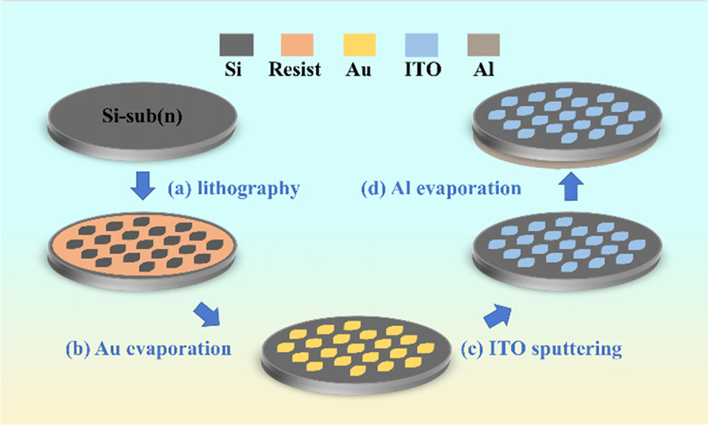
Figure 1 illustrates the process flow of making ITO/Au/n-Si SPDs. The PDs were fabricated with a commercial epi-ready n-type (0.1–1 Ω·cm, μ) silicon substrate. First, the PD areas were defined by ultraviolet lithography using a negative resist (AR-U 4030) in leaf patterns with an area of . Before being sent to the electron beam evaporation (Ohmiker-50B) chamber for Au deposition at room temperature, the patterned substrates were dipped in a dilute HF solution ( for 1 min) for oxide removing. During the evaporation process, the deposition pressure was maintained below and the deposition rate was 0.17 Å/s (1 Å = 0.1 nm) controlled by the current with a voltage at 8 kV. In addition, the plate where the substrates were placed rotated at a rate of 8 r/min to ensure the uniformity of the film. After that, 100 nm ITO was immediately deposited on the Au film by a double chamber magnetron sputtering system (Shenyang Defeng Technology) at room temperature under atmosphere. During the sputtering process, the thickness was controlled by the sputtering time with a deposition rate of 0.93 Å/s. Finally, the ohmic contact on the backside was realized by a 300 nm Al film using Ohmiker-50B with a deposition rate of 1.7 Å/s at room temperature after removing the oxide by a dilute HF solution ( for 1 min). To protect the ITO/Au electrode from the HF solution, the positive resist (AZ 6130) was used as the protective layer during the removing process. The source of Au and Al in the Ohmiker-50B was the molten metal that came from the particles (purity, 99%; particles diameter, 0.5 cm) by heating an electron beam in the crucible before evaporating; the source of the ITO was a bulk target (purity, 99.99%; In2O3:SnO2 = 9:1, mass ratio).
Sign up for Photonics Research TOC. Get the latest issue of Photonics Research delivered right to you!Sign up now
Figure 1.Schematic process flow for the formation of ITO/Au/n-Si SPDs. (a) The PD areas were defined on an n-type Si substrate by ultraviolet lithography. (b) The patterned Si was sent to the electron beam evaporation chamber to grow Au film at room temperature. (c) 100 nm ITO was deposited on the Au film immediately by a double chamber magnetron sputtering system at room temperature under atmosphere. (d) The ohmic contact on the backside was realized by a 300 nm Al film using electron beam evaporation.
The surface morphology of the ITO/Au/n-Si PDs was analyzed using a field-emission scanning electron microscope (SEM) (SUS5500) monitored with accelerating voltage (30 kV) and an atomic force microscope (AFM) (Bruker, Multimode8) in a ScanAsyst mode. While the interfaces between the ITO, Au, and n-Si substrate were analyzed by the SEM (SUS5500) and high resolution transmission electron microscope (HRTEM) (JEM-2200FS). The transmission spectra were acquired by a UV-VIS-NIR light spectrophotometer (Shimadzu, UV 3600 Plus). Since the Si substrate is opaque in nature, the ITO layer (100 nm) and the ITO (100 nm)/Au (2 nm, 3 nm, 4 nm, 6 nm) multilayers, processed in the same manner as their Si counterparts, were deposited on glass substrates to obtain the transmission of the electrodes. In addition, the transmission of the glass had been removed during the transmission measurement. At the same time, the resistivity of the ITO/Au/glass was analyzed by a Hall effect testing instrument.
The I–V measurements were performed by the use of a Keithley 4200 in the forward and reverse regions at by 10 mV per step, while the temperature dependent I–V characteristics were acquired by a standard electrical probe station (Lakeshore Cryotronics) and a Keithley 4200 semiconductor parameter analyzer from to 1 V by a step of 10 mV. In addition, the photocurrent at the certain wavelength was obtained with a Keithley 4200 from to 2 V when the detector was normally incident by 1064 nm (2 mW) or 1310 nm laser (1 mW). In order to study the response of the detector to a wide range of wavelengths, the Fourier photocurrent spectrum of the device was measured with the Bruker V70. When the photocurrent was measured, the distance between the light source and the PDs was kept constant, and the position of the PDs was adjusted on the plane until the maximum photocurrent occurred to ensure consistency of test conditions.
3. RESULTS AND DISCUSSION
In this study, silicon-based SPDs with two design structures are firstly prepared: (1) ITO (100 nm)/Au (6 nm)/n-Si SPD (our target detector) and (2) reference ITO (100 nm)/n-Si PD, referred to as 6AuSPD and 0AuSPD, respectively. The left side of Fig. 2(a) shows the cross-sectional SEM image of the 6AuSPD. The ITO thickness is about 100 nm, while the top-view SEM images of the two AuSPDs on the right suggest that the surface of the ITO becomes a little mottled and rough after Au insertion; this will be demonstrated later in an AFM test. The HRTEM is used to study the Au insertion layer in detail; the Au thickness is about 6 nm, as clearly seen in Fig. 2(b). Furthermore, it can also be clearly seen that a clear and smooth interface between the ITO and the Au is obtained. Figure 2(c) shows that in the AFM images (area: μμ) the root-mean-square (RMS) roughness increases from 0.624 nm of bare ITO (almost the same as with the Si substrate) to 1.32 nm, indicating that the insertion of the Au slightly decreases the surface flatness of the electrode. The main reason for the roughness increment may be the poor film compactness of Au caused by the low atomic energy and the low growth rate during deposition [35]. In order to study the optoelectronic performance of the detectors, the current–voltage characteristics were analyzed under dark (room and low temperature) and light (room temperature) conditions according to the schematic diagram displayed in Fig. 2(d).
Figure 2.(a) Cross-sectional scanning electron microscope (SEM) image of the 6AuSPD on the left, and a top view of the SEM images of the 0AuSPD (top) and 6AuSPD (down) in an area of μμ on the right. (b) Cross-sectional high resolution transmission electron microscope (HRTEM) images of the 6AuSPD. (c) Atomic force microscope (AFM) images (scanned area: μμ) of the 0AuSPD (left) and the 6AuSPD (right). (d) Schematic diagram of the current–voltage measurement for SPDs.
Both SPDs exhibit typical rectifying characteristics, as shown in Fig. 3(a). The current is limited by the barrier in the junction under the reverse bias while rising quickly and becoming limited by the series resistance under the forward bias since the barrier is gradually compensated by the applied voltage. In addition, by linear extrapolation, the turn-on voltages for the PDs were extracted, as seen from the inset in Fig. 3(a), as 0.1 V and 0.33 V, respectively, which means the larger SB for the SPD with the Au insertion layer. In the J–V semi-log plot [see Fig. 3(b)], it can be clearly seen that the dark current density of the SPD with the Au insertion layer decreases significantly (7876 times). The dark current density is about at , which is only one-sixth of the reported data, while the rectifying ratio ( at ) is 300 times higher than that reported by other literature [16]. Furthermore, the temperature dependent I–V measurement was carried out to extract the SBH. As shown in Fig. 3(c), the current density grows with increasing temperature at reverse bias, consistent with what is expected for thermionic emission in an SPD [23]. Figure 3(d) shows the good linear correlation for extracted versus 1000/T Richardson plots, where the SBH of 6AuSPD together with 0.434 eV of 0AuSPD is extracted, respectively, following the procedure described in the literature [36]. The potential barrier formed by Au and silicon in our work is consistent with the value reported in other research [37]. As a matter of fact, the difference of work functions between ITO and n-Si (0.1–1 Ω·cm) is about 0.57 eV, while the difference between Au and n-Si (0.1–1 Ω·cm) is about 0.87 eV. These results suggest that such a low dark current density must be attributed to the SBH increment, which results from the thin Au insertion layer.
Figure 3.(a) Room temperature J–V characteristics on a linear scale for the 0AuSPD and 6AuSPD under dark conditions; the inset map is the corresponding J–V data from to 0.4 V. (b) Room temperature J–V characteristics in semi-log for the 0AuSPD and 6AuSPD. (c) Temperature dependent J–V characteristics for the 6AuSPD. (d) In () versus 1000/T for the 0AuSPD and 6AuSPD. Experimental photocurrents and dark currents for the 0AuSPD and 6AuSPD with (e) a 1310 nm laser at a power of 1 mW and (f) a 1064 nm laser at a power of 2 mW.
Figure 4.(a) Room temperature J–V characteristics in semi-log for AuSPDs under dark conditions; (b) ln () versus 1000/T for AuSPDs. (c) Photoresponse of AuSPDs measured at zero bias voltage from 1100 to 1700 nm. (d) Experimental photocurrents for AuSPDs with 1310 nm wavelength measured from to 0.3 V. (e) The dark current, photocurrent, and photocurrent-to-dark-current ratio of AuSPDs at a bias of , 1310 nm, and power of 1 mW.
The photocurrents of the detectors measured at the wavelength of 1310 nm and 1064 nm are shown in Figs. 3(e) and 3(f), respectively. Because of the high dark current density of the 0AuSPD, it is difficult to distinguish the photocurrent from the dark current under an illumination of 1310 nm. Instead, the dark current and the photocurrent of 6AuSPD are obviously separated with a contrast ratio of more than 1000:1, which benefits from the sharp decline of dark current. Furthermore, stronger absorption occurs under the illumination of 1064 nm due to the addition of inter-band absorption. The dark current and photocurrent can be distinguished in both PDs, but the stronger contrast in the PD with the Au insertion layer indicates the higher sensitivity.
Generally, the proportion of light entering the junction is important to the responsivity of the metal/semiconductor detector, so it is necessary to reduce the Au thickness to improve the transmission of the top electrode with no other performance recession. Therefore, another three SPDs with 4 nm, 3 nm, and 2 nm Au insertion layers were prepared; they are referred to as 4AuSPD, 3AuSPD, and 2AuSPD, respectively. More details about the transmission, uniformity, and resistivity of the top electrodes and morphology related to the Au thickness can be found in Appendix A. Overall, all ITO/Au films exhibit a considerable uniformity and good conductivity [see Appendix A, Figs. 5(b) and 6]. And with the decrease of Au thickness, the transmission as well as the surface smoothness becomes better [see Appendix A, Fig. 7(a)]. When the thickness of Au is reduced to 2 nm, the average transmission increases to about 80% from 850 nm to 1550 nm and the RMS also decreases to 0.683 nm. This indicates that the reduction of Au is of great significance to improve the light transmittance and surface smoothness without damaging the conductivity of the electrodes.
Figure 5.(a) Samples were measured using a UV-VIS-NIR light spectrophotometer with light normal to the surface. (b) The corresponding photographs of these ITO/Au/glass films were taken under incandescent light with continuous spectrum showing considerable process uniformity in .
Figure 7.(a) AFM images of the top electrodes in the 2AuSPD, 3AuSPD, 4AuSPD, and 6AuSPD with a scanned area of 5 μm × 5 μm. (b) Cross-sectional HRTEM images of the 2AuSPD, 3AuSPD, 4AuSPD, and 6AuSPD.
Figure 8.Schematic diagram of the responsivity measurement for the 2AuSPD. A 1310 nm laser with a power of 2 mW was emitted through a single-mode fiber with an inner diameter of 9 μm onto the 2AuSPD arrays. The distance between the detector and the optical fiber outlet was about 2 mm and the numerical aperture () of the fiber was 0.11, leading to a spot with a diameter of 450 μm on the detector.
The J–V relationship of AuSPDs with different Au thicknesses is plotted in Fig. 4(a). Overall, each device clearly established rectifying behavior. What excited us is that these detectors had a similar low dark current density of approximately at , which resulted from almost the same SBHs (0.797, 0.801, 0.803, 0.795 eV for Au thickness 2–6 nm) extracted from the ln () versus 1000/T curves in Fig. 4(b). Furthermore, the low dark current and high SBH of 2AuSPD indicate that a continuous Au plane has been formed to effectively prevent the diffusion of ITO to Si due to the good film-forming ability of Au [38], which can also be verified in Appendix A [see Fig. 7(b)]. In a word, reducing the Au thickness can greatly improve the electrode transmission without damaging the dark current performance of the device.
The photoresponse of these AuSPDs is measured at zero bias voltage for wavelength varying from 1100 nm to 1700 nm, as shown in Fig. 4(c). Overall, the response increases with the decrease of Au thickness within the range of the measured wavelength. Two obvious absorption edges determined by silicon intrinsic bandgap (1.12 eV) at 1110 nm and the SBH (0.795 eV) at 1560 nm are clearly observed, suggesting that the detection is realized through both inter-band and internal photoemission. To further confirm the effect of Au thickness on the response of near-infrared, these detectors were also measured at 1310 nm with a low power excitation (), as shown in Fig. 4(d). The photocurrent of 2AuSPD is nearly twice that of 6AuSPD, which also can verify the above conclusion. In addition, the response improvement is more obvious as the Au layer decreases from 6 nm to 4 nm, which is consistent with the results of the electrode transmission in Appendix A [see Figs. 5(a) and 5(b)], fully demonstrating that the raising response mainly benefits from the improvement of the transparency of the electrodes. A more comprehensive display of the performance improvement can be found in Fig. 4(e), including the dark current, the photocurrent at measured under 1310 nm, and the photocurrent-to-dark current ratio (PDR) of AuSPDs. The PDR is defined as where and are the photocurrent and dark current, respectively. The PDR values for all samples (Au thickness: 0–6 nm) are 1, 4625, 4440, 4510, and 3833, respectively. It is clearly seen that the PDR of AuSPDs is significantly improved due to the effective suppression of , which contributes to the high SBH from the Au insertion layer. Meanwhile, 2AuSPD has the best PDR due to the best transmission of 2 nm Au. The properties of 2AuSPD are summarized in Table 1, together with those of other silicon-based SPDs used for telecommunication wavelength for comparison. In comparison with the Au/Si SPDs supporting surface plasmon polaritons and other special design SPDs such as the addition of graphene or using pyramidally shaped Si in Table 1, these AuSPDs with simple processing exhibit the lower dark current density, leading to a better detection performance [32–34,40]. We also investigated other designs that use higher SBH to suppress the dark current density of SPDs, such as NiSi/n-Si, ITO/CuO/n-Si, ITO/Ag/n-Si or ITO/AgNWs/ITO/p-Si [25,29,31,41]. Apart from the lower dark current density, the AuSPDs exhibit an unprecedented high rectification ratio, as well as a better normalized photocurrent-to-dark current ratio (NPDR). The value of responsivity for the 2AuSPD was acquired from the method in Appendix A (see Fig. 9). In addition, the responsivity spectra as well as the external quantum efficiency spectra with different biases of all AuSPDs are also observed, as shown in Appendix A (see Fig. 10). The responsivity and quantum efficiency of the AuSPDs are related to the bias voltage, which is consistent with the photocurrents of different biases at 1310 nm in Fig. 4(d). Moreover, the AuSPDs have a high response speed and can reach sub-GHz, as shown in Appendix A (see Fig. 11).
Configuration
Special Design
SBH (eV)
Dark Current Density (A/cm2) (at −1V)
Rectification Ratio (at ±1V)
Responsivity (mA/W) (at −1V)
NPDR (mW−1) (at −1V)
Refs.
Au/n-Si
SPP/waveguide
0.31
6.0
57 (ρ∼15Ω·cm)
13.3 at 1310 nm
3.8×10² at 1310 nm
[32]
Au/graphene/p-Si
SPP/waveguide
0.34
1.3
∼150 (ρ∼0.05Ω·cm)
85 at 1550 nm
4.25×10³ at 1550 nm
[33]
Au/p-Si
SPP/grating
0.32
48.0
∼40 (ρ∼5Ω·cm)
14.5 at 1550 nm
0.048 at 1550 nm
[34]
Graphene/p-Si
∼4.5
∼160 (ρ∼5Ω·cm)
∼4.6 at 1550 nm (−4V)
∼8.6 at 1550 nm
[39]
Al/p-Si pyramids
Si pyramids
0.6
29.0
∼103 (ρ∼15Ω·cm)
12 at 1300 nm
96 at 1300 nm
[40]
Cu/p-Si
Waveguide
0.74
2.2×10⁻⁵
∼50 (lightly doped)
0.08 at 1550 nm
4.7 at 1550 nm
[22]
NiSi/n-Si
0.62
1.2×10⁻⁵
∼105 (ρ∼5Ω·cm)
7.4 at 1310 nm
7.4×10² at 1310 nm
[41]
ITO/CuO/n-Si
0.5
8.0×10⁻⁶
∼10 (ρ∼5Ω·cm)
0.0075 at one sun illumination
[31]
ITO/AgNWs/ITO/p-Si
NWs
0.71
5.0×10⁻⁵
421 (ρ∼5Ω·cm)
∼280 at 1310 nm
[29]
ITO/Ag/n-Si
0.74
2.4×10⁻⁶
4×10⁵ (ρ∼0.5Ω·cm)
62 at 1310 nm (0 V)
∼6.2×10⁴ at 1310 nm (0 V)
[25]
Our work
0.795
3.7×10⁻⁷
1.5×10⁸ (ρ∼0.5Ω·cm)
27 at 1310 nm
1.04×10⁵ at 1310 nm
Table 1. Performance Comparison for Silicon-Based SPDs
Figure 10.(a) Responsivity spectra with different biases of all AuSPDs. The values of the responsivities have been calibrated with a 1310 nm laser. (b) External quantum efficiency spectra with different biases of all AuSPDs.
In conclusion, we have demonstrated a silicon-based internal-photoemission AuSPD with a record low dark current density operating in a broad wavelength range. Since implementation of a thin Au insertion layer can effectively increase the SBH and suppress the dark current, the fabricated device showed a dark current density of at and a high rectification ratio of at . Furthermore, we found that the responsivity was obviously improved without costing the dark current performance of the device by reducing the Au thickness, resulting in an increase of the PDR and thus an overall performance enhancement of silicon-based SPD. We believe that the demonstrated device is a step forward in merging silicon technology and internal photoemission with simple design and high efficiency for optical communication bands.
Acknowledgment
Acknowledgment. The authors wish to acknowledge the assistance on the Fourier photocurrent spectrum received from the Key Laboratory of Semiconductor Materials Science, Institute of Semiconductors, Chinese Academy of Science.
APPENDIX A: CHARACTERIZATION OF AUSPDs
Transmission Spectrum as a Function of Au Thickness and Photographs Taken under Incandescent Light of the ITO/Au/Glass Films
The transmission of ITO/Au/ITO film was characterized by the UV-VIS-NIR light spectrophotometer. Since the Si substrate is opaque in nature, the ITO layer (100?nm) and the ITO (100?nm)/Au (2?nm, 3?nm, 4?nm, 6?nm) multilayers, processed in the same manner as their Si counterparts, were deposited on glass substrates to obtain the transmission profile of the top electrodes. It can be seen from Fig.?5(a) that all samples show a considerable transmission over a broad wavelength range (400–1800?nm), and with the reduction of the thickness of Au film, the transmission is significantly improved due to the increment of the incoming light. When the thickness of Au is reduced to 2?nm, the average transmission is about 80% from 850?nm to 1550?nm, and specifically, the transmission can be increased to 85% for 1310?nm wavelength. Here, the increased fluctuation near 900?nm is caused by replacing the external detector of the spectrophotometer during the test. Furthermore, the corresponding photographs of these ITO/Au/glass films in Fig.?5(b) were taken under incandescent light with continuous spectrum, the color of which not only reveals the reflection of the Au film but also shows the considerable process uniformity in .
Resistivity of ITO/Au Films on Glass
Resistivity of ITO/Au films deposited on glass as a function of Au thickness is shown in Fig.?6. The resistivity of only ITO film is , while the resistivity values of hybrid ITO/Au films are 4.346?×?10–4, 4.361?×?10–4, 4.532?×?10–4, and , respectively. These results suggest that a thin Au insertion layer could slightly improve the conductivity that may result from a better contact between Au and silicon. However, increasing Au from 2?nm to 6?nm does not significantly decrease the resistivity due to the good conductivity of ITO. In this case, the small resistivity variation of ITO/Au films with different Au thicknesses is probably caused by the experimental error of Hall measurement.
AFM Images and Cross-Sectional HRTEM Images
The RMS values of the corresponding AFM images are 0.683?nm, 0.732?nm, 0.982?nm, and 1.33?nm, respectively, as shown in Fig.?7(a). As Au thickness decreases from 6?nm to 2?nm, the RMS of the electrodes is decreased from 1.32?nm to 0.683?nm. Furthermore, it can be clearly seen in Fig.?7(b) that approximately 2?nm, 3?nm, 4?nm, and 6?nm Au layers, respectively, are observed between ITO and n-Si, which are consistent with our design.
Schematic Diagram of Responsivity Measurement for the 2AuSPD
During the test, the Al electrode on the back of the AuSPD is adhered to the silicon substrate plated with μm thick Au layer using conductive silver glue, and then connected with Keithley 4200 through the lead wire (Al, 50?μm). As seen in Fig.?8, the effective light receiving area under the light spot is about half the whole electrode except the lead wire joint. Considering that the effective receiving area of the detector is about one-third of the spot area and the light is not normally incident to the electrode, the optical power coupled into the detector may be lower by an order of magnitude.
Experimental Photocurrent for the 2AuSPD with 1310?nm Wavelength
The photocurrent under 1310?nm for 2AuSPD is at , as shown in Fig.?9. Considering the effective receiving area and the optical power coupled into it mentioned in Fig.?8, the responsivity () of the whole electrode is approximately where and are the photocurrent and optical power coupled into the effective receiving area, respectively.
Responsivity Spectra and External Quantum Efficiency Spectra with Different Biases of All AuSPDs
The external quantum efficiency () is defined as follows: where , , , , and are the responsivity, Planck constant, velocity of light, elementary charge, and wavelength of incident light, respectively. Thus, the external quantum efficiency spectra under different biases exhibit a similar trend as the responsivity spectra. As shown in Fig.?10, all the AuSPDs show the same variation behavior of the responsivities [Fig.?10(a)] and the external quantum efficiencies [Fig.?10(b)] under the different bias voltages. They nearly keep constant under the bias of 0?V to , while they decrease a lot with the bias of 0.2?V due to the opposite direction of the photogenerated electric field and the built-in electric field. All the responsivity spectra under different biases exhibit two obvious absorption edges corresponding to the inter-band and internal photoemission, which are the same as those in Fig.?4(c). Additionally, it can be seen from the responsivity spectra of different Au insertion layers that the responsivity is inversely proportional to the thickness of the Au layer. The responsivity increases obviously with the thinning Au layer, which mainly results from the increase of the light transmittance of the electrode.
Response Time Measurement of the AuSPDs at 1310??nm
The response speeds of all the AuSPDs are obtained by analyzing the transient response spectra, as shown in Fig.?11. The AuSPDs are inspired by the femtosecond amplifier laser system (SOL Ace, Spectra-Physics) with 100?fs pulse width, and the wavelength was set at 1310?nm. The Tektronix TDS3054C digital phosphor oscilloscope (500?MHz) is used for the photocurrent recorder. The response consists of a peak with full width at half maximum of 2?ns, accompanied by a longer timescale tail. The decay of the photocurrent can be fitted by the bi-exponential Eq.?(A3) as reported [42]: where , , are the pre-exponential factors and , are decay time constants, respectively. The values of , with the fitting curve are 1.24?ns and 3.06?ns for 2AuSPD, 1.24?ns and 2.49?ns for 3AuSPD, 0.97?ns and 2.00?ns for 4AuSPD, and 1.78?ns and 4.35?ns for 6AuSPD, respectively. It can be concluded that the response time of all devices is on the order of ns, and the rise time is shorter from the response curve. These results suggest that the response of the AuSPDs is fast enough to reach the sub-GHz response level.
References
[1] D. Prather, S. Shi, J. Murakowski, G. Schneider, A. Sharkawy, C. Chen, B. Miao. Silicon-Based Photonic Crystal Structures: From Design to Realization, 47-93(2008).
Xinxin Li, Zhen Deng, Jun Li, Yangfeng Li, Linbao Guo, Yang Jiang, Ziguang Ma, Lu Wang, Chunhua Du, Ying Wang, Qingbo Meng, Haiqiang Jia, Wenxin Wang, Wuming Liu, Hong Chen, "Hybrid nano-scale Au with ITO structure for a high-performance near-infrared silicon-based photodetector with ultralow dark current," Photonics Res. 8, 1662 (2020)