Contents
2020
Volume: 8 Issue 12
20 Article(s)

Export citation format
PEROVSKITE PHOTONICS
Engineering a light–matter strong coupling regime in perovskite-based plasmonic metasurface: quasi-bound state in the continuum and exceptional points
Leran Lu, Quynh Le-Van, Lydie Ferrier, Emmanuel Drouard, Christian Seassal, and Hai Son Nguyen
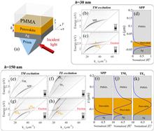
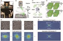
We present theoretically the formation of exciton&ndash;photon polaritons and exciton-surface plasmon polaritons in a perovskite-based subwavelength lattice on the metallic plane. It is shown that the later polaritons will be achieved as the perovskite layer is ultra-thin (<50 nm), while the co-existence of both polaritons will dominate, as the thickness of the perovskite metasurface approaches wavelength-scale. In the two cases, the lower polaritonic branches consist of dark and bright modes corresponding to infinite and finite radiative quality factors, respectively. Another salient property in this work is that it allows one to obtain exceptional points (EPs) in momentum space with a four-fold enhancement of local density of states through engineering the perovskite metasurface. Our findings show that the perovskite metasurface is an attractive and rich platform to make polaritonic devices, even with the presence of a lossy metallic layer.
Photonics Research
  • Publication Date: Nov. 12, 2020
  • Vol. 8, Issue 12, A91 (2020)
TOPOLOGICAL PHOTONICS AND BEYOND
Weak-value amplification for the optical signature of topological phase transitions
Weijie Wu, Shizhen Chen, Wenhao Xu, Zhenxing Liu, Runnan Lou, Lihua Shen, Hailu Luo, Shuangchun Wen, and Xiaobo Yin
We show that weak measurements can be used to measure the tiny signature of topological phase transitions. The signature is an in-plane photonic spin Hall effect, which can be described as a consequence of a Berry phase. It is also parallel to the propagation direction of a light beam. The imaginary part of the weak value can be used to analyze ultrasmall longitudinal phase shifts in different topological phases. These optical signatures are related to the Chern number and bandgaps; we also use a preselection and postselection technique on the spin state to enhance the original signature. The weak amplification technique offers a potential way to determine the spin and valley properties of charge carriers, Chern numbers, and topological phases by direct optical measurement.
Photonics Research
  • Publication Date: Nov. 05, 2020
  • Vol. 8, Issue 12, B47 (2020)
Reviews
Instrumentation and Measurements
Emerging micro-additive manufacturing technologies enabled by novel optical methods
Wei Lin, Dihan Chen, and Shih-Chi Chen
This paper presents a comprehensive review of recent advances in micro-additive manufacturing enabled by novel optical methods with an emphasis on photopolymerization-based printing processes. Additive manufacturing, also known as three-dimensional (3D) printing, has become an important engineering solution to construct customized components or functional devices at low cost. As a green manufacturing technology, 3D printing has the advantages of high energy efficiency, low material consumption, and high precision. The rapid advancement of 3D printing technology has broadened its applications from laboratory research to industrial manufacturing. Generally, 3D objects to be printed are constructed digitally [e.g., via computer-aided design (CAD) programs] by connecting a 3D dot array, where a dot is defined as a voxel through mechanical, electrical, or optical means. The voxel size ranges from a few orders of magnitude of the wavelength of light to the sub-diffraction limit, achieved by material nonlinearity and precise power thresholding. In recent years, extensive research in optical additive manufacturing has led to various breakthroughs in quality, rate, and reproducibility. In this paper, we review various micro-3D printing techniques, including single-photon and two-photon processes, with a focus on innovative optical methods, e.g., ultrafast beam shaping, digital holography, and temporal focusing. We also review and compare recent technological advances in serial and parallel scanning systems from the perspectives of resolution, rate, and repeatability, where the strengths and weaknesses of different methods are discussed for both fundamental and industrial applications.
Photonics Research
  • Publication Date: Nov. 12, 2020
  • Vol. 8, Issue 12, 1827 (2020)
Integrated Optics
Advances in on-chip photonic devices based on lithium niobate on insulator | Editors' Pick
Jintian Lin, Fang Bo, Ya Cheng, and Jingjun Xu
Crystalline lithium niobate (LN) is an important optical material because of its broad transmission window that spans from ultraviolet to mid-infrared and its large nonlinear and electro-optic coefficients. Furthermore, the recent development and commercialization of LN-on-insulator (LNOI) technology has opened an avenue for the realization of integrated on-chip photonic devices with unprecedented performances in terms of propagation loss, optical nonlinearity, and electro-optic tunability. This review begins with a brief introduction of the history and current status of LNOI photonics. We then discuss the fabrication techniques of LNOI-based photonic structures and devices. The recent revolution in the LN photonic industry has been sparked and is still being powered by innovations of the nanofabrication technology of LNOI, which enables the production of building block structures, such as optical microresonators and waveguides of unprecedented optical qualities. The following sections present various on-chip LNOI devices categorized into nonlinear photonic and electro-optic tunable devices and photonic-integrated circuits. Some conclusions and future perspectives are provided.
Photonics Research
  • Publication Date: Nov. 30, 2020
  • Vol. 8, Issue 12, 1910 (2020)
Research Articles
Imaging Systems, Microscopy, and Displays
Resolution-enhanced intensity diffraction tomography in high numerical aperture label-free microscopy
Jiaji Li, Alex Matlock, Yunzhe Li, Qian Chen, Lei Tian, and Chao Zuo
We propose label-free and motion-free resolution-enhanced intensity diffraction tomography (reIDT) recovering the 3D complex refractive index distribution of an object. By combining an annular illumination strategy with a high numerical aperture (NA) condenser, we achieve near-diffraction-limited lateral resolution of 346 nm and axial resolution of 1.2 μm over 130 μm×130 μm×8 μm volume. Our annular pattern matches the system’s maximum NA to reduce the data requirement to 48 intensity frames. The reIDT system is directly built on a standard commercial microscope with a simple LED array source and condenser lens adds-on, and promises broad applications for natural biological imaging with minimal hardware modifications. To test the capabilities of our technique, we present the 3D complex refractive index reconstructions on an absorptive USAF resolution target and Henrietta Lacks (HeLa) and HT29 human cancer cells. Our work provides an important step in intensity-based diffraction tomography toward high-resolution imaging applications.
Photonics Research
  • Publication Date: Nov. 12, 2020
  • Vol. 8, Issue 12, 1818 (2020)
Confocal visible/NIR photoacoustic microscopy of tumors with structural, functional, and nanoprobe contrasts
Jiangbo Chen, Yachao Zhang, Xiaozhen Li, Jingyi Zhu, Dengfeng Li, Shengliang Li, Chun-Sing Lee, and Lidai Wang
Distinguishing early-stage tumors from normal tissues is of great importance in cancer diagnosis. We report fiber-based confocal visible/near-infrared (NIR) optical-resolution photoacoustic microscopy that can image tumor microvasculature, oxygen saturation, and nanoprobes in a single scanning. We develop a cost-efficient single laser source that provides 532, 558, and 1064 nm pulsed light with sub-microseconds wavelength switching time. Via dual-fiber illumination, we can focus the three beams to the same point. The optical and acoustic foci are confocally aligned to optimize the sensitivity. The visible and NIR wavelengths enable simultaneous tumor imaging with three different contrast modes. Results show obvious angiogenesis, significantly elevated oxygen saturation, and accumulated nanoparticles in the tumor regions, which offer comprehensive information to detect the tumor. This approach also allows us to identify feeding and draining vessels of the tumor and thus to determine local oxygen extraction fraction. In the tumor region, the oxygen extraction fraction significantly decreases along with tumor growth, which can also assist in tumor detection and staging. Fiber-based confocal visible/NIR photoacoustic microscopy offers a new tool for early detection of cancer.
Photonics Research
  • Publication Date: Nov. 19, 2020
  • Vol. 8, Issue 12, 1875 (2020)
Instrumentation and Measurements
Long-distance ranging with high precision using a soliton microcomb | On the Cover
Jindong Wang, Zhizhou Lu, Weiqiang Wang, Fumin Zhang, Jiawei Chen, Yang Wang, Jihui Zheng, Sai T. Chu, Wei Zhao, Brent E. Little, Xinghua Qu, and Wenfu Zhang
Laser-based light detection and ranging (lidar) plays a significant role in both scientific and industrial areas. However, it is difficult for existing lidars to achieve high speed, high precision, and long distance simultaneously. Here, we demonstrate a high-performance lidar based on a chip-scaled soliton microcomb (SMC) that can realize all three specialties simultaneously. Aided by the excellent properties of ultrahigh repetition rate and the smooth envelope of the SMC, traditional optical frequency comb (OFC)-based dispersive interferometry is heavily improved and the measuring dead zone induced by the mismatch between the repetition rate of the OFC and resolution of the optical spectrum analyzer is totally eliminated. Combined with an auxiliary dual-frequency phase-modulated laser range finder, the none-dead-zone measurable range ambiguity is extended up to 1500 m. The proposed SMC lidar is experimentally implemented in both indoor and outdoor environment. In the outdoor baseline field, real-time, high-speed (up to 35 kHz) measurement of a long distance of ~1179 m is achieved with a minimum Allan deviation of 5.6 μm at an average time of 0.2 ms (27 nm at an average time of 1.8 s after high-pass filtering). The present SMC lidar approaches a compact, fast, high-precision, and none-dead zone long-distance ranging system, aimed at emerging applications of frontier basic scientific research and advances in industrial manufacturing.
Photonics Research
  • Publication Date: Nov. 30, 2020
  • Vol. 8, Issue 12, 1964 (2020)
Integrated Optics
Compact and broadband multimode waveguide bend by shape-optimizing with transformation optics | Spotlight on Optics
Shuyi Li, Lifeng Cai, Dingshan Gao, Jianji Dong, Jin Hou, Chunyong Yang, Shaoping Chen, and Xinliang Zhang
Multimode waveguide bend is one of the key components for realizing high-density mode-division multiplexing systems on chip. However, the reported multimode waveguide bends are either large, bandwidth-limited or fabrication-complicated, which hinders their applications in future high-density multimode photonic circuits. Here we propose a compact multimode waveguide bend supporting four TE modes simply by shape-optimizing with transformation optics. The shape of the waveguide is optimized in the virtual space with gradient distribution of the refractive index, so that the scattering loss and intermode cross talk are well suppressed. After conformal mapping back into the physical space, a compact (effective radius of 17 μm) multimode bending waveguide is obtained. Simulations show that the proposed multimode waveguide bend has little loss (0.1 dB) and low cross talk (-20 dB) throughout an ultrabroad wavelength range of 1.16–1.66 μm. We also fabricated the shape-optimized multimode bending waveguide on a silicon-on-insulator wafer. At 1550 nm wavelength, the measured excess losses for the four lowest-order TE modes are less than 0.6 dB, and the intermode cross talks are all below -17 dB. Our study paves the way for realizing high-density and large-scale multimode integrated optical circuits for optical interconnect.
Photonics Research
  • Publication Date: Nov. 17, 2020
  • Vol. 8, Issue 12, 1843 (2020)
Bias-drift-free Mach–Zehnder modulators based on a heterogeneous silicon and lithium niobate platform | Editors' Pick
Shihao Sun, Mingbo He, Mengyue Xu, Shengqian Gao, Ziyan Chen, Xian Zhang, Ziliang Ruan, Xiong Wu, Lidan Zhou, Lin Liu, Chao Lu, Changjian Guo, Liu Liu, Siyuan Yu, and Xinlun Cai
Optical modulators have been and will continue to be essential devices for energy- and cost-efficient optical communication networks. Heterogeneous silicon and lithium niobate modulators have demonstrated promising performances of low optical loss, low drive voltage, and large modulation bandwidth. However, DC bias drift is a major drawback of optical modulators using lithium niobate as the active electro-optic material. Here, we demonstrate high-speed and bias-drift-free Mach–Zehnder modulators based on the heterogeneous silicon and lithium niobate platform. The devices combine stable thermo-optic DC biases in silicon and ultra-fast electro-optic modulation in lithium niobate, and exhibit a low insertion loss of 1.8 dB, a low half-wave voltage of 3 V, an electro-optic modulation bandwidth of at least 70 GHz, and modulation data rates up to 128 Gb/s.
Photonics Research
  • Publication Date: Nov. 30, 2020
  • Vol. 8, Issue 12, 1958 (2020)
Lasers and Laser Optics
Quantum dot mode-locked frequency comb with ultra-stable 25.5 GHz spacing between 20°C and 120°C | Spotlight on Optics
Shujie Pan, Jianou Huang, Zichuan Zhou, Zhixin Liu, Lalitha Ponnampalam, Zizhuo Liu, Mingchu Tang, Mu-Chieh Lo, Zizheng Cao, Kenichi Nishi, Keizo Takemasa, Mitsuru Sugawara, Richard Penty, Ian White, Alwyn Seeds, Huiyun Liu, and Siming Chen
Semiconductor mode-locked lasers (MLLs) are promising frequency comb sources for dense wavelength-division-multiplexing (DWDM) data communications. Practical data communication requires a frequency-stable comb source in a temperature-varying environment and a minimum tone spacing of 25 GHz to support high-speed DWDM transmissions. To the best of our knowledge, however, to date, there have been no demonstrations of comb sources that simultaneously offer a high repetition rate and stable mode spacing over an ultrawide temperature range. Here, we report a frequency comb source based on a quantum dot (QD) MLL that generates a frequency comb with stable mode spacing over an ultrabroad temperature range of 20–120°C. The two-section passively mode-locked InAs QD MLL comb source produces an ultra-stable fundamental repetition rate of 25.5 GHz (corresponding to a 25.5 GHz spacing between adjacent tones in the frequency domain) with a variation of 0.07 GHz in the tone spacing over the tested temperature range. By keeping the saturable absorber reversely biased at -2 V, stable mode-locking over the whole temperature range can be achieved by tuning the current of the gain section only, providing easy control of the device. At an elevated temperature of 100°C, the device shows a 6 dB comb bandwidth of 4.81 nm and 31 tones with >36 dB optical signal-to-noise ratio. The corresponding relative intensity noise, averaged between 0.5 GHz and 10 GHz, is -146 dBc/Hz. Our results show the viability of the InAs QD MLLs as ultra-stable, uncooled frequency comb sources for low-cost, large-bandwidth, and low-energy-consumption optical data communications.
Photonics Research
  • Publication Date: Nov. 30, 2020
  • Vol. 8, Issue 12, 1937 (2020)
First experimental demonstration of coherent beam combining of more than 100 beams
Hongxiang Chang, Qi Chang, Jiachao Xi, Tianyue Hou, Rongtao Su, Pengfei Ma, Jian Wu, Can Li, Man Jiang, Yanxing Ma, and Pu Zhou
Photonics Research
  • Publication Date: Nov. 30, 2020
  • Vol. 8, Issue 12, 1943 (2020)
Optical and Photonic Materials
High detectivity photodetectors based on perovskite nanowires with suppressed surface defects
Guohui Li, Rui Gao, Yue Han, Aiping Zhai, Yucheng Liu, Yue Tian, Bining Tian, Yuying Hao, Shengzhong Liu, Yucheng Wu, and Yanxia Cui
Solution-processable, single-crystalline perovskite nanowires are ideal candidates for developing low-cost photodetectors, but their detectivities are limited due to a high level of unintentional defects. Through the surface-initiated solution-growth method, we fabricated high-quality, single-crystalline, defects-suppressed MAPbI3 nanowires, which possess atomically smooth side surfaces with a surface roughness of 0.27 nm, corresponding to a carrier lifetime of 112.9 ns. By forming ohmic MAPbI3/Au contacts through the dry contact method, high-performance metal–semiconductor–metal photodetectors have been demonstrated with a record large linear dynamic range of 157 dB along with a record high detectivity of 1.2×10¹⁴ Jones at an illumination power density of 5.5 nW/cm2. Such superior photodetector performance metrics are attributed to, first, the defects-suppressed property of the as-grown MAPbI3 nanowires, which leads to a quite low noise current in the dark, and second, the ohmic contact between MAPbI3 and Au interfaces, which gives rise to an improved responsivity compared with the Schottky contact counterpart. The realized high-performance MAPbI3 nanowire photodetector advances the development of low-cost photodetectors and has potential applications in weak-signal photodetection.
Photonics Research
  • Publication Date: Nov. 19, 2020
  • Vol. 8, Issue 12, 1862 (2020)
Superior third-order nonlinearity in inorganic fullerene-like WS2 nanoparticles
Tianlun Li, Rui Hao, Lingling Zhang, Jianyong Mao, Feng Li, Yanpeng Zhang, Jixiang Fang, and Lei Zhang
Two-dimensional (2D) transition metal dichalcogenides (TMDs) attain increasing attention due to their exceptional nonlinear optical efficiencies, which hold promising potential for on-chip photonics and advanced optoelectronic applications. Planar TMDs have been proven to support orders-higher third-order nonlinear coefficients in comparison with common nonlinear materials. Interestingly, stronger light–matter interaction could be motivated when curved features are introduced to 2D TMDs. Here, a type of inorganic fullerene-like WS2 nanoparticles is chemically synthesized using hard mesoporous silica. By using the spatial self-phase modulation (SSPM) method, the nonlinear refractive index n2 and third-order susceptibility χ(3) are investigated in the visible range. It is found that n2~10-5 cm2/W and χ(3)~10-7 esu, two orders higher than the counterparts of planar WS2 structures. Our experimental findings provide a fresh thinking in designing nonlinear optical materials and endow TMDs with new potentials in photonic integration applications.
Photonics Research
  • Publication Date: Nov. 20, 2020
  • Vol. 8, Issue 12, 1881 (2020)
Comparison of growth structures for continuous-wave electrically pumped 1.55 μm quantum dash lasers grown on (001) Si
Wei Luo, Ying Xue, Jie Huang, Liying Lin, Bei Shi, and Kei May Lau
Semiconductor lasers directly grown on silicon offer great potential as critical components in high-volume, low-cost integrated silicon photonics circuits. Although InAs/InP quantum dash (QDash) lasers on native InP substrate emitting at 1.5 μm (C-band) have demonstrated notable performance, the growth of InAs/InP QDash lasers on silicon remains undeveloped because of the 8% lattice mismatch between InP and silicon. Here we report advances of growth techniques leading to the first C-band room-temperature continuous-wave electrically pumped QDash lasers on CMOS standard (001) silicon substrates by metalorganic chemical vapor deposition. A correlation between various material characterizations and device performance is analyzed for different QDash laser structures grown on planar nominal (001) silicon. With the optimized QDash growth and improved fabrication process, the lowest threshold current density of 1.5 kA/cm2 was determined on an 8 μm×1.5 mm device on planar silicon with a single facet output power exceeding 14 mW. The device results illustrate the good material quality of the QDash lasers grown on silicon, suggesting potential applications for other active components of photonic integrated circuits, such as semiconductor optical amplifiers, modulators, and photodetectors.
Photonics Research
  • Publication Date: Nov. 20, 2020
  • Vol. 8, Issue 12, 1888 (2020)
Optoelectronics
High-performance fiber-integrated multifunctional graphene-optoelectronic device with photoelectric detection and optic-phase modulation
Linqing Zhuo, Pengpeng Fan, Shuang Zhang, Yuansong Zhan, Yanmei Lin, Yu Zhang, Dongquan Li, Zhen Che, Wenguo Zhu, Huadan Zheng, Jieyuan Tang, Jun Zhang, Yongchun Zhong, Wenxiao Fang, Guoguang Lu, Jianhui Yu, and Zhe Chen
In graphene-based optoelectronic devices, the ultraweak interaction between a light and monolayer graphene leads to low optical absorption and low responsivity for the photodetectors and relative high half-wave voltage for the phase modulator. Here, an integration of the monolayer graphene onto the side-polished optical fiber is demonstrated, which is capable of providing a cost-effective strategy to enhance the light–graphene interaction, allowing us to obtain a highly efficient optical absorption in graphene and achieve multifunctions: photodetection and optical phase modulation. As a photodetector, the device has ultrahigh responsivity (1.5×10⁷ A/W) and high external quantum efficiency (>1.2×10⁹%). Additionally, the polybutadiene/polymethyl methacrylate (PMMA) film on the graphene can render the device an optical phase modulator through the large thermo-optic effect of the PMMA. As a phase modulator, the device has a relatively low half-wave voltage of 3 V with a 16 dB extinction ratio in Mach–Zehnder interferometer configuration.
Photonics Research
  • Publication Date: Nov. 30, 2020
  • Vol. 8, Issue 12, 1949 (2020)
Silicon Photonics
Nonlinear silicon photonics on CMOS-compatible tellurium oxide
Neetesh Singh, Hamidu M. Mbonde, Henry C. Frankis, Erich Ippen, Jonathan D. B. Bradley, and Franz X. Kärtner
Silicon photonics is coming of age; however, it is still lacking a monolithic platform for optical sources and nonlinear functionalities prompting heterogeneous integration of different materials tailored to different applications. Here we demonstrate tellurium oxide as a complementary metal oxide semiconductor silicon photonics platform for nonlinear functionalities, which is already becoming an established platform for sources and amplifiers. We show broadband supercontinuum generation covering the entire telecom window and show for the first time to our knowledge third-harmonic generation in its integrated embodiment. Together with the now-available lasers and amplifiers on integrated TeO2 this work paves the way for a monolithic TeO2-based nonlinear silicon photonics platform.
Photonics Research
  • Publication Date: Nov. 30, 2020
  • Vol. 8, Issue 12, 1904 (2020)
Spectroscopy
Doppler velocimeter based on dual-comb absorption spectroscopy
Chenglin Gu, Xing Zou, Zhong Zuo, Daowang Peng, Yuanfeng Di, Yang Liu, Daping Luo, and Wenxue Li
The determination of airflow parameters is essential to the research of critical information on environment monitoring, chemical kinetics, and aerodynamic and propulsion applications. During the past few decades, tunable diode laser absorption spectroscopy has become a common and efficient tool for the flow velocity measurement based on the Doppler shift of the absorption line. Dual-comb absorption spectroscopy (DCAS), as a state-of-the-art Fourier-transform broadband spectroscopic technique, not only can detect multiple trace molecules in parallel but also can extract Doppler shifts to derive the flow velocity through the analysis of dozens of molecular absorption lines simultaneously with high precision. Here, we report a proof-of-principle demonstration of the velocity measurements of acetylene at various flow velocities by means of a high-resolution and broadband DCAS. Mode-resolved Doppler-shifted rotational-vibrational lines in the P branch of acetylene molecules are obtained. A model for multiline Doppler frequency determination is investigated and experimentally verified. The flow velocity measurements with a measuring uncertainty down to the submeter per second over the range from 8.7 m/s to 44.8 m/s at an effective time resolution of 1 s and a measuring uncertainty of 1.97 m/s at 0.1 s are demonstrated. With broadband mid-infrared frequency combs covering atmospheric transmission windows, the open-path measurement for monitoring diffusion of the weak pollutant source would be realized.
Photonics Research
  • Publication Date: Nov. 23, 2020
  • Vol. 8, Issue 12, 1895 (2020)
Surface Optics and Plasmonics
Boosting a sub-10 nm nanogap array by plasmon-triggered waveguide resonance
Yu Tian, Hailong Wang, Yijia Geng, Lili Cong, Yu Liu, Weiqing Xu, and Shuping Xu
Gap-type metallic nanostructures are widely used in catalytic reactions, sensors, and photonics because the hotspot effect on these nanostructures supports giant local electromagnetic field enhancement. To achieve hotspots, researchers devote themselves to reducing gap distances, even to 1 nm. However, current techniques to fabricate such narrow gaps in large areas are still challenging. Herein, a new coupling way to boost the sub-10 nm plasmonic nanogap array is developed, based on the plasmon-triggered optical waveguide resonance via near-field coupling. This effect leads to an amplified local electromagnetic field within the gap regions equivalent to narrower gaps, which is evidenced experimentally by the surface-enhanced Raman scattering intensity of probed molecules located in the gap and the finite-difference time-domain numerical simulation results. This study provides a universal strategy to promote the performance of the existing hotspot configurations without changing their geometries.
Photonics Research
  • Publication Date: Nov. 17, 2020
  • Vol. 8, Issue 12, 1850 (2020)

About the Cover

A long-distance ranging system with chip-scale integration potential is developed using soliton pulses generated from an on-chip microcavity, and high-speed, highly accurate and real-time ranging is experimentally demonstrated at long distance of more than 1179 m.