1MOE Key Laboratory of Material Physics and Chemistry under Extraordinary Conditions, and Shaanxi Key Laboratory of Optical Information Technology, School of Physical Science and Technology, Northwestern Polytechnical University, Xi’an 710072, China
2Institute for Photonics and Advanced Sensing, University of Adelaide, Adelaide, SA 5005, Australia
3ARC Centre of Excellence for Nanoscale BioPhotonics, University of Adelaide, Adelaide, SA 5005, Australia
4Institute of Photonics Technology, Jinan University, Guangzhou 510632, China
5Institute of Laser Engineering, Beijing University of Technology, Beijing 100124, China
Plasmonic devices using periodic metallic nanostructures have recently gained tremendous interest for color filters, sensing, surface enhanced spectroscopy, and enhanced photoluminescence, etc. However, the performance of such plasmonic devices is severely hampered by the solid substrates supporting the metallic nanostructures. Here, a strategy for freestanding metallic nanomembranes is introduced by taking advantages of hollow substrate structures. Large-area and highly uniform gold nanomembranes with nanohole array are fabricated via a flexible and simple replication-releasing method. The hollow structures include a hollow core fiber with 30 μm core diameter and two ferrules with their hole diameter as 125 and 500 μm, respectively. As a proof-of-concept demonstration, 2 times higher sensitivity of the bulk refractive index is obtained with this platform compared to that of a counterpart on a solid silica substrate. Such a portable and compact configuration provides unique opportunities to explore the intrinsic properties of the metal nanomembranes and paves a new way to fabricate high-performance plasmonic devices for biomolecule sensing and color filter.
1. INTRODUCTION
Since the pioneering work on subwavelength metal hole arrays in 1998 [1], the last decades have witnessed a tremendous growth in their theoretical characterizations and experimental demonstrations [2–4]. The extraordinary optical transmission (EOT), refractive index sensitivity, local field enhancement, and operation window of the nanohole arrays can be tailored flexibly by manipulating the periodicity, diameter, shape, and filling materials within the nanoholes [5–8]. This outstanding tunability evokes substantial interest in nanophotonic and plasmonic applications based on metal nanostructures, such as color filters [9], sensing [10–12], surface enhanced spectroscopy [13,14], and enhanced photoluminescence [15,16].
Along with these extensive studies, though, most attention has been paid to metal nanohole arrays on planar substrates [2,17,18] or optical fiber end faces [19] due to their easy fabrication and reliable performance. Critical issues arise from the solid supporting substrates that have significant impacts on the properties of the metal nanohole arrays. For instance, the transmission efficiency is limited by the solid substrate due to the destructive interference among evanescent modes or impedance mismatch at the metal and substrate interface [20]. High absorption of silicon dioxide substrate imposes an undesirable constraint on the practical applications in the mid-infrared range [21].
In order to reduce this substrate effect, some efforts have been made based on substrate engineering, such as using near-zero-epsilon materials as the substrates [22,23] and elaborating the substrate with complex structures or compositions [24,25]. Fabricating metal nanostructures on high pedestals can not only suppress the undesirable impacts of the substrate, but also improve the field overlap with analytes [26–28]. More recent works show that rationally designed quasi-freestanding [29–31] or freestanding [32] metal nanohole arrays fabricated through advanced techniques can also effectively address the substrate issue. However, fabrication of highly uniform and periodic metal nanostructures with large lateral size is cost-prohibitive and time-consuming in conventional ways, i.e., via electro- or ion-beam lithography [33]. It is still a pending matter to achieve freestanding metal nanomembrane in applicable configurations for practical applications.
Sign up for Photonics Research TOC. Get the latest issue of Photonics Research delivered right to you!Sign up now
To this end, herein, we report a new class of freestanding nanomembranes with nanohole arrays supported by hollow substrate structures, including a hollow core fiber (HCF) and hollow ferrules. The method used to pattern gold nanohole arrays is a replication-releasing procedure we developed very recently [34], where large-area gold nanomembranes were made. The released nanomembrane is transferred onto the end face of the hollow substrates. The flexible access to both sides of the freestanding nanomembrane enables a significantly enhanced interaction between the analyte and the nanomembrane compared to a counterpart on a solid silica substrate. Enhanced optical transmission and a doubled sensitivity in refractive index sensing are demonstrated. Taking advantages of the flexibility and simplicity, this strategy paves a new efficient way to explore the intrinsic properties of substrate-free nanomembranes and facilitate portable applications such as color filters and biochemical sensing with high performance.
2. FABRICATION OF THE FREESTANDING GOLD NANOMEMBRANE
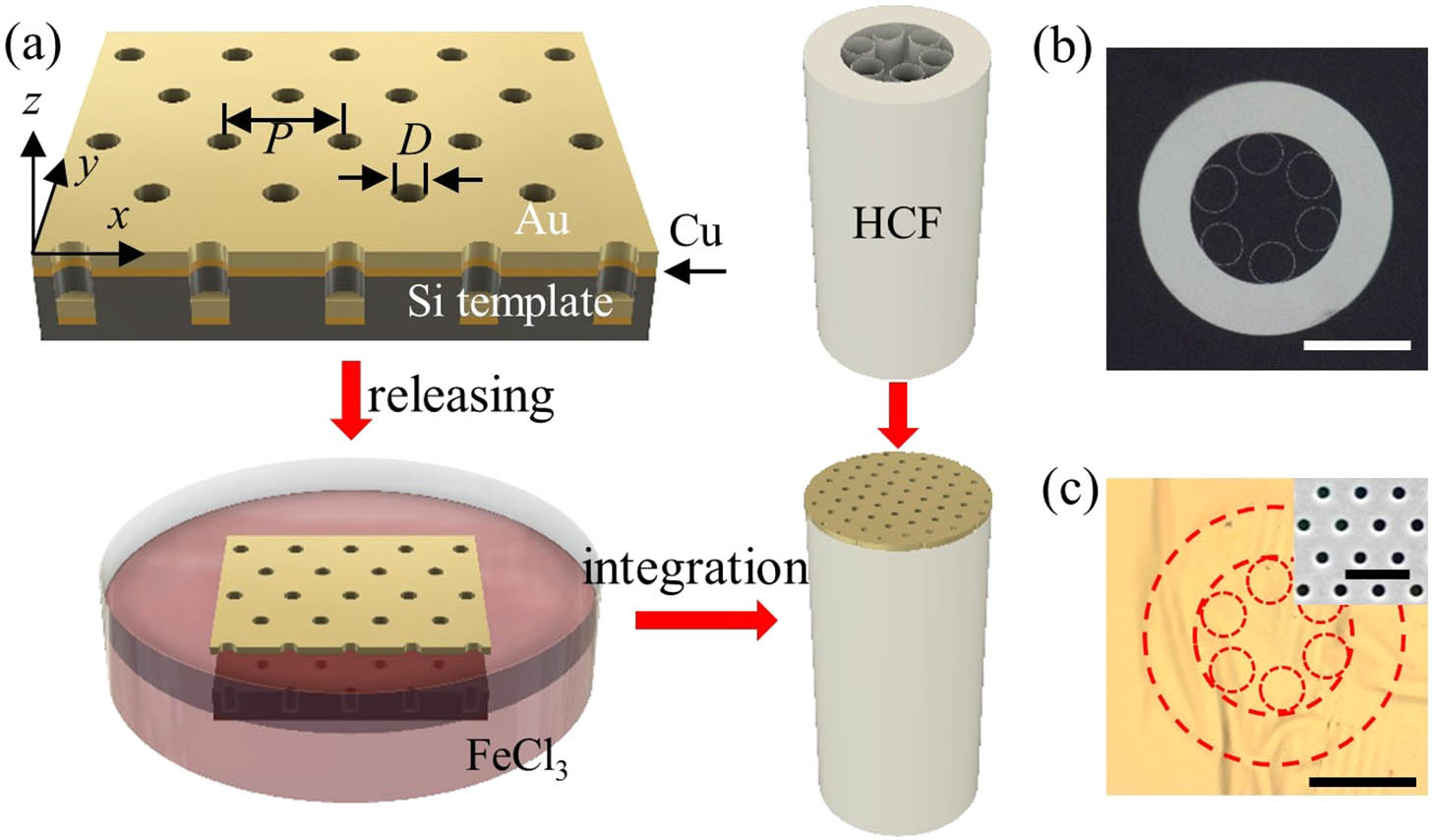
In order to demonstrate the flexible fabrication of the freestanding gold nanomembranes, three hollow substrates, including one HCF and two ferrules with different hole sizes, were tested. As a portable platform for practical applications, the HCF was focused unless otherwise specified. Figure 1(a) shows the schematic of the fabrication process of the freestanding nanomembrane. A prepatterned silicon template with a hexagonal array of nanoholes was used to deposit a 50 nm-thick copper and a 100 nm-thick gold layer sequentially. The deposition rate was maintained at 0.1 nm/s. The array periodicity , nanohole diameter , and the hole depth in the template are 600, 200, and 350 nm, respectively. These dimensions are chosen in order to comply with the accessible window of our spectrometer, realize narrow bandwidths, and avoid connection between the deposited nanomembranes on top of the template and the nanodisks at the bottom of the nanoholes. The metal-deposited template was then immersed into solution to etch the copper layer so that the gold nanomembrane was released for transfer. Using an in-house fabricated single-mode HCF to pick up the released gold layer with care, the strong van der Waals force maintained the attachment of the gold nanomembrane onto the end face of the HCF with minimum wrinkle. Therefore, a freestanding gold nanomembrane on the HCF was obtained. Note that since the released gold nanomembrane is significantly larger than the tip area of the HCF or ferrules, the transferred gold nanomembrane is normally wrapped around the tip. For schematic simplification, only a gold nanomembrane on the end face of the HCF is shown in Fig. 1(a). The corresponding micrographs of the HCF and the freestanding gold nanomembrane on the HCF are presented in Figs. 1(b) and 1(c). The outer and inner diameters of the silica jacket of the HCF are 125 and 75 μm, respectively. Six thin silica capillaries with 500 nm wall thickness and 20 μm diameter in the cladding confine the light within the hollow core with 30 μm diameter. The scanning electron microscopy (SEM) image of the gold nanomembrane in Fig. 1(c) inset clearly shows the hexagonal pattern of the nanoholes. The surface roughness of the gold nanomembrane is in nanoscale due to the inherent polycrystallinity of the evaporation process [12,34].
Figure 1.(a) Schematic diagram of the fabrication process of the freestanding gold nanomembrane. Photographs of the (b) HCF and (c) freestanding gold nanomembrane on HCF. The dashed circles indicate the profile of the HCF beneath the gold nanomembrane. Scale bars, 50 μm; inset, SEM image of the gold nanomembrane (scale bar, 1 μm).
A three-dimensional finite-difference time-domain (FDTD) simulation (FDTD Solutions, Lumerical Solutions Inc.) was conducted to investigate the resonance behaviors of the gold nanomembrane with two configurations: freestanding and a counterpart sitting on fused silica (, refractive index 1.46). As shown in the Fig. 2(a) inset, the structures were illuminated by a normal plane wave along the axis with polarization direction along the axis. Periodic boundary conditions were set in and directions, while along the axis, a perfectly matched layer was used to minimize unnecessary boundary reflections. The dielectric permittivity data taken from Ref. [35] were used for the gold film.
Figure 2.(a) Simulated transmission spectra of the gold nanohole arrays with different configurations in air; insets, simulated electrical field distributions overlaid with the Poynting vectors at 500 nm in the plane (left) and transmission spectrum of a nanohole described by classical aperture theory (right); (b) calculated (dashed lines) and simulated (2D mapping) dispersion relations of the freestanding nanomembrane in air.
The simulated transmission spectra of the freestanding gold nanomembrane and the counterpart on in air are plotted in Fig. 2(a). The transmission maximum of the freestanding gold nanomembrane is nearly 2 times as large as that of the -based counterpart. This originates from the reduced coupling efficiency of the surface plasmons at the upper air/gold and lower silica/gold interfaces in substrate-based configurations [36]. Additionally, the transmission of an isolated nanohole of 200 nm diameter in a 100 nm-thick gold film predicted by a classic aperture theory [37] is shown in the inset of Fig. 2(a). It scales as , where is the radius of the nanohole and is the wavelength of the incident light. Accordingly, the transmission is on the order of . Therefore, the transmission of the freestanding gold nanohole arrays is significantly enhanced by 55 times at the resonance wavelength of 650 nm compared to that predicted by the classic aperture theory, referring to the EOT phenomenon.
Although the EOT arises from a complex mechanism of surface plasmon excitation and geometric effects (termed as a spoof plasmon) [2,18], in a first approximation the resonance wavelength positions of the nanohole array can be derived from the momentum conservation in the interaction of the incident photons and the surface plasmon polaritons as [3,38,39] where is the wave vector of the excited surface plasmon, is the component of the incident wave vector that lies in the plane of the interface, is the angle of incidence with respect to the interface normal, are the reciprocal lattice vectors of the hexagonal array of nanoholes, and and are integers, representing the scattering orders of the array. Thus, Eq. (1) reduces to and the resonance position of maxima is given by where and are the dielectric constants of the metal and the dielectric medium in contact with the metal. This relationship also gives a qualitative guide for the positions of transmission minima [40].
According to Eq. (3), with the incidence angle varying, the resonance positions will shift so that the dispersion relation of the freestanding gold nanohole array in air can be obtained as depicted by the dashed lines in Fig. 2(b). The resonance peak splits into two peaks that move in opposite directions, indicating two modes of , respectively. The FDTD simulation results are recorded as presented by the two-dimensional (2D) mapping in Fig. 2(b). Because the associated scattering loss of the nanoholes and the interference due to the presence of the nanoholes are neglected in the analytical relations of Eqs. (1)–(3), resonance peaks are located at higher energies than in simulated results [3]. In addition, the freestanding configuration is symmetric, which supports the excitation of only one set of transmission peaks in air. Therefore, freestanding nanomembranes are more promising in color filters because of a higher purity of filtered color than the asymmetric counterparts on substrates that produce two sets of peaks in the transmission spectrum at asymmetric upper and lower nanohole array interfaces [41].
To reveal the origin beneath the spectrum of the freestanding gold nanomembrane, near-field profiles are desired. Poynting vectors indicate the spatial energy flows, and is the most dominant component of the corresponding electrical field, from which the distributions of oscillating charge densities can be determined with positive or negative signs. As shown in the Fig. 2(a) inset, the electrical field throughout the nanohole and the “laminar” Poynting vectors clearly confirms the nature of direct light propagation from one side of the nanohole to the other at the wavelength of 500 nm [42]. The dipolar electrical field distribution of the nanohole array in the plane (μ) reveals the highly localized field around the rims of the nanohole, associated with a dipole oscillation mode of the freestanding gold nanomembrane at 653 nm [Fig. 3(a)]. The field distributions overlaid with the Poynting vectors, and the component of the electrical field in the plane at 576 and 653 nm corresponding to transmission minimum and maximum in Fig. 2(a), respectively, are shown in Fig. 3(b). The resonance behaviors at 576 and 653 nm are different. For , the electric field is mostly concentrated at the interface of air and gold, decaying with distance along the direction, while the confined Poynting vectors indicate that the mode energy does not contribute to the transmission, consistent with the transmission minimum. The symmetric profiles at both air/gold interfaces imply that the coupling oscillations are tangent to the plane of the nanohole array. This spectral characteristic is associated with Wood’s anomaly [43]. For , the large enhancement of the local field mainly exists at the rims of the gold nanohole. The self-guiding Poynting vectors throughout the nanohole confirm the high-efficiency propagation of the energy through the gold nanomembrane, corresponding to the transmission maximum. The strong coupling to transmission is regarded as a superradiant state [40]. The asymmetric profiles at two air/gold interfaces reflect the different charge distribution at 653 nm compared with 576 nm as well. The field distribution of the cross section [μ, dashed line in Fig. 3(b)] along at 653 nm is shown in Fig. 3(c). The field decays exponentially from the air/gold interface, and the decay length was determined to be 20 nm.
Figure 3.(a) Simulated electrical field distribution at 653 nm in the plane; (b) field distributions overlaid with the Poynting vectors (top) and component of the corresponding electrical field (bottom) at 576 and 653 nm [transmission minimum and maximum in Fig. 2(a), respectively] in the plane, and (c) field distribution of the cross section [μ, dashed line in (b)] along at 653 nm of the freestanding nanomembrane in air; (d) simulated electrical field distributions overlaid with the Poynting vectors at 627 nm (top) and 841 nm (bottom) in the plane of the gold nanomembrane on in air.
As a comparison to the field distributions of the freestanding gold nanomembrane, the simulated electrical field distributions overlaid with the Poynting vectors at 627 and 841 nm in the plane of the gold nanomembrane on substrate in air are depicted in Fig. 3(d). The asymmetric enhancement of the fields at air/gold and silica/gold interfaces reveals that the resonances at 627 and 841 nm correspond to the air/gold and silica/gold resonance modes, respectively.
The simulated spectra of the freestanding gold nanomembrane and the counterpart on in water are plotted in Fig. 4(a). Apart from the peak around 500 nm originating from the direct transmission of gold film as discussed above, a more complex spectrum emerges compared to that in air. This can be attributed to the overlapping and coupling among resonance modes [33]. The dispersion relation of the freestanding nanomembrane in water obtained from simulations and analytical prediction in Eq. (3) is shown in Fig. 4(b). Two branches associated with modes are excited.
Figure 4.(a) Simulated transmission spectra of the gold nanohole arrays with different configurations in water; (b) calculated (dashed lines) and simulated (2D mapping) dispersion relations of the freestanding nanomembrane in water.
As shown in Fig. 5(a), the large enhancement of the local fields and the “whirlpools” Poynting vectors indicate the excitations of surface plasmons at 610, 742, and 837 nm in water, respectively [42], while the “flow-over” Poynting vectors contribute to the high transmission at 610 and 837 nm, respectively. The profile at 610 nm implies that the nanoholes act as nanoantennas collecting the incident light at upper corners and then re-emit it into the free space. The near-field profiles at 742 and 837 nm in water are symmetric and asymmetric, while the corresponding electrical field distributions are asymmetric and symmetric, respectively [2]. The resonance at 837 nm is correlated to the characteristic mode of the freestanding gold nanomembrane. The field distributions in the plane also confirm the resonance characteristics at 742 and 837 nm, respectively [Fig. 5(b)]. As depicted by the cross-section field distributions along the direction [μ, dashed lines in Fig. 5(a)] in Fig. 5(c), the decay lengths at 742 and 837 nm are 45 and 24 nm, respectively. This feature manifests that localized surface plasmon resonance (LSPR) possesses more localized field than the bulk surface plasmon resonance (SPR).
Figure 5.(a) Simulated electrical field distributions overlaid with the Poynting vectors (top) and component of the corresponding electrical field (bottom) at 610, 742, and 837 nm in the plane; (b) field distribution at 742 and 837 nm in the plane, and (c) field distributions of the cross section [μ, dashed lines in (a)] along at 742 and 837 nm of the freestanding gold nanomembrane in water. The resonance at 837 nm corresponds to the maximum transmission in Fig. 4(a).
To demonstrate the high performance of the freestanding gold nanomembrane in refractive-index sensing, experimental and theoretical results are depicted in Fig. 6. Various refractive indices (1.3330, 1.3418, 1.3505, 1.3594, and 1.3684) were obtained using different concentrations of NaCl water solutions (0, 5%, 10%, 15%, and 20%, respectively). As schematically shown in the Fig. 6(a) inset, the white light was coupled to the HCF from the end with the gold nanomembrane integrated, and the transmitted light out of the HCF was collected by another multimode fiber connected to a spectrometer. In measurements, the HCF and illumination/collection fiber were mounted on three-dimensional stages to keep the gap of the two opposite end faces of the two fibers around 2 mm, and each individual solution was dropped within the gap to change the refractive index surrounding the gold nanomembrane. The relatively large open-geometry of the nanoholes facilitates small molecules of water penetrating into the hollow substrate. The experimental spectra are found to be in a reasonable agreement with the simulated ones, apart from a complex spectral shape around 750 nm appearing in the experiments, while in the simulations, a single peak at 742 nm exists [Figs. 6(a) and 6(c)]. This divergency might be because the gold nanomembrane that is integrated on the end face of the HCF is not perfectly flat [Fig. 1(c)] [44], causing a large dissipation through joule loss and scattering loss [45]. In addition, according to Eq. (3), the slightly nonnormal incidence in HCF might be another factor that contributes to the spectral divergency.
Figure 6.Experimental (a) spectral evolution, (b) wavelength shifts and corresponding simulated (c) spectra, (d) wavelengths of the freestanding gold nanomembrane to varied refractive index. Experimental (e) spectral evolution, (f) wavelength shifts and corresponding simulated (g) spectra, (h) wavelengths of a gold nanomembrane on a solid silica fiber end face to varied refractive index.
Two resonance modes around 750 and 810 nm were monitored to test the sensitivity. It is shown that both modes proportionally shift to longer wavelengths as the refractive index increases, as plotted in Fig. 6(b). Linear fittings of the wavelength shifts were conducted to obtain the refractive index sensitivities, which are 472 nm per refractive index unit (RIU) and 436 nm/RIU, respectively, for both modes. The small error bars (standard deviations of the wavelengths) show that the proposed device exhibits good stability and repeatability. Remarkably, even though the experimental sensitivities are slightly smaller than the simulated values of 540 nm/RIU and 578 nm/RIU [Fig. 6(d)], respectively, roughly doubled sensitivities are achieved for the freestanding gold nanomembrane compared with the measured 298 nm/RIU (simulated 254 nm/RIU) of a counterpart on a solid silica fiber end face with a core diameter of 200 μm in Figs. 6(e)–6(h). Table 1 summarizes the typical performances of various plasmonic sensors based on nanohole arrays. The freestanding nanomembrane on the HCF exhibits moderate sensitivities and figure of merit (FOM sensitivity/linewidth, a widely accepted performance indicator for plasmonic sensors). Compared with that on our solid fiber with core diameter of 200 μm, the FOM of the freestanding nanomembrane on the 30 μm core diameter HCF can be further improved by tailoring the core diameter of the HCF and developing the transfer quality. In addition, the new and portable kind of freestanding metal nanomembranes enabled by HCF is promising in more applications than sensing.
Principle
Sensitivity (nm/RIU)
FOM (RIU−1)
Reference
Solid substrate
70.9–681
0.86–50
[4,46–48]
Fiber coupled
180–559
10–55
[49–51]
Complex substrate
473–671
2.23–42
[24,25]
Quasi-freestanding
630
40
[52]
Freestanding
–
0.795
[21]
Solid fiber coupled
298
33
This work
Freestanding on HCF
472/436
26/11
Table 1. Comparison of Performances among Various Plasmonic Sensors Based on Nanohole Arrays
The replication-releasing method guarantees the high quality and consistency of the nanomembrane fabrication. In addition, according to our previous work [34], the flexible freestanding gold nanomembrane has an in-plane modulus of around 200 GPa. This provides the freedom of the integration of freestanding gold nanomembranes onto large hollow supporting substrates without cracking. To demonstrate this merit, we deployed them onto various supports and characterized the optical properties of diverse freestanding configurations based on the similar principle of fabrication as with HCF above.
Figure 7(a) shows the reflection spectra of the freestanding gold nanomembranes supported by the HCF and two hollow ferrules with 75, 125, and 510 μm in hole diameters, respectively. The measurement schematic is present in the Fig. 7(a) inset, where, as mentioned above in the transmission mode, the gap between the illumination fiber and the HCF was adjusted to be by three-dimensional stages. A dip around the wavelength of 500 nm was observed in all cases, which is the inherent feature of gold as discussed above. Additionally, another two dips at wavelengths of 572 and 653 nm emerged in the simulated spectrum. The open circles and red dots correlate with the corresponding resonance modes between experiments and simulations, respectively. The larger the hole diameter of the supporting substrate is, the closer the agreement between the experiment and simulation is found. This can be attributed to different boundary conditions in simulation and reality [45]. The lateral boundary condition in the simulations is a periodic boundary condition, which gives rise to an infinitely extended nanomembrane in the plane. In contrast, the measuring area in the experiments is finitely restricted to the hole diameter of the supporting components.
Figure 7.(a) Reflection spectra of the freestanding gold nanomembranes based on various configurations. The red dots and open circles indicate the corresponding resonance modes in experiments and simulations, respectively. (b) Evolution of the reflection spectra and (c) resonance wavelength shifts of the freestanding gold nanomembrane on the 125 μm hollow ferrule to varied refractive index; (d) simulated refractive index response of the freestanding gold nanomembrane.
Furthermore, we demonstrated the refractive-index response of the freestanding nanomembrane on the 125 μm hollow ferrule. As shown in Figs. 7(b) and 7(c), sensitivities of 418 nm/RIU and 461 nm/RIU are obtained, in terms of the wavelength shifts of different resonance modes as linear functions of the refractive index. The experimental sensitivities are slightly smaller than the simulated values [Fig. 7(d)], though, consistent with the results using the HCF through transmission monitoring above. After repeated measurements, no considerable degradation was observed for the freestanding gold nanomembrane, indicating the excellent stability and repeatability in this aqueous sensing case.
4. CONCLUSIONS
In conclusion, we presented a new class of freestanding metal nanomembranes, which is realized by using hollow supporting substrates. Due to the completely substrate-free configuration, enhanced optical performances were obtained. Specifically, we showed a doubled sensitivity in refractive-index sensing compared with a substrate-based counterpart, which is attributed to the free access of analytes to both sides of the freestanding nanomembrane. A series of FDTD simulations were conducted to reveal the resonance characteristics of related modes. Moreover, the freestanding nanomembrane is free and versatile to integrate with diverse supports for tunable functionalities. Such a flexible platform is robust and highly compatible within existing all-fiber circuits, and therefore opens a new avenue of exploring the intrinsic properties of metallic nanomembranes and facilitating practical applications such as color filters and biomolecule detections with higher sensitivities and lower detection limits compared to the same nanomembranes sitting on solid substrates.
Acknowledgment
Acknowledgment. This work was performed in part at the Optofab Node of the Australian National Fabrication Facility (ANFF), a company established under the National Collaborative Research Infrastructure Strategy to provide nano- and microfabrication facilities for Australia’s researchers. The authors appreciate Xinyu Wang (Yanshan University and University of Adelaide) for technical assistance in HCF operation.