
Shihao Sun, Mingbo He, Mengyue Xu, Shengqian Gao, Ziyan Chen, Xian Zhang, Ziliang Ruan, Xiong Wu, Lidan Zhou, Lin Liu, Chao Lu, Changjian Guo, Liu Liu, Siyuan Yu, Xinlun Cai. Bias-drift-free Mach–Zehnder modulators based on a heterogeneous silicon and lithium niobate platform[J]. Photonics Research, 2020, 8(12): 1958
- Photonics Research
- Vol. 8, Issue 12, 1958 (2020)
Abstract
1. INTRODUCTION
By harnessing the tool sets and process flows in complementary metal–oxide–semiconductor (CMOS) foundries based on silicon-on-insulator (SOI) platforms, silicon photonics (SiPh) promises advantages of low cost, high volume, and reliable manufacturing [1–3] and therefore may create a radically new landscape for photonic integrated circuits (PICs). This makes it very attractive for applications in future transceivers in telecommunication and data communication [4], in which fast, energy-efficient, and low-loss electro-optical (EO) modulators are crucial components [5,6]. As an essential component, optical modulators on SiPh platforms commonly use the plasma dispersion effect in silicon junctions [7–10]. With this technology, various impressive devices have been developed, leading to commercial 100 Gb/s optical transceivers for the telecom and datacom applications [11]. However, the plasma dispersion effect has intrinsic limitations in modulation bandwidth and optical loss. In particular, because of free carrier absorption, silicon junctions do not support pure phase modulation, which deteriorates the fidelity of signals in advanced modulation formats. The current performance envelope of the silicon optical modulator is believed to be more or less close to their physical limits, but future applications require even higher performance due to the insatiable demands of data capacity.
To overcome the drawbacks inherent in silicon modulators, a diverse range of materials offering better modulation performance have been heterogeneously co-integrated onto the SiPh platform, including graphene [12], EO polymers [13], indium phosphide (InP) [14], and barium titanate (BTO) [15]. Besides these materials, lithium niobate (LN), the most successful material for high-speed optical modulation [16–22], has also been integrated with SOI circuits by the die-to-wafer bonding technique [23–26]. Recently, we have demonstrated a heterogeneous LN/SOI Mach–Zehnder modulator (MZM) [27], which exhibits low insertion loss , large bandwidth , and a single line rate of up to 112 Gb/s using four-level pulse amplitude modulation (PAM-4).
In general, a DC bias needs to be applied to set the MZM at an optimum operating point for best performance. For example, the optimum bias point is the quadrature point for PAM-4. In our previous work, as in the vast majority of cases, the bias point was set by applying a DC voltage across an EO phase shifter (EOPS) in an LN waveguide. However, the electro-optically controlled bias point in LN modulators may change over time: this phenomenon is the so-called DC bias drift [28], which is related to the flow and redistribution of electrical charge in the LN region under the application of the DC voltage and is an inevitable problem for an LN MZM that requires dedicated monitoring photodetectors (PDs) and control circuitry in practical devices [29–31].
Sign up for Photonics Research TOC. Get the latest issue of Photonics Research delivered right to you!Sign up now
Here, we report a high-performance heterogeneous LN/SOI MZM, featuring stable operation that is substantially free of the DC bias drift phenomena. A thermo-optic phase shifter (TOPS) on silicon waveguide is used to achieve stable DC bias. Although the thermo-optic (TO) bias method can be achieved on LN [32], the larger TO coefficient of silicon makes the TOPS power-efficient and compact in size. In addition, the present device shows a large EO bandwidth of , a low half-wave voltage of 3 V, and low on-chip insertion loss of . On–off keying (OOK) modulation up to 100 Gb/s and PAM-4 up to 128 Gb/s are successfully demonstrated.
2. METHOD
Schematics of the hybrid LN modulator are shown in Fig. 1. The hybrid platform consists of an SOI substrate (220 nm silicon, 3 μm buried oxide layer) with a 600 nm thick layer of x-cut LN membranes on the top surface through benzocyclobuten (BCB) adhesive die-to-wafer bonding. The modulator can be divided into two parts. Part I is the passive silicon optical input/output (I/O) circuit, including a shallow etch grating coupler, 3 dB multimode interferometer (MMI), and silicon waveguides. Part II is the high-speed modulation region including LN waveguides, which form the arms of the Mach–Zehnder interferometer (MZI) and the laterally spaced gold traveling-wave electrodes (TWEs) with ground-signal-ground (GSG) configuration. Vertical adiabatic couplers formed by silicon inverse tapers and superimposed LN waveguides are used to interface between Parts I and II. The TOPS consists of titanium (Ti) heating electrodes and is located alongside the silicon waveguides in Part I, as depicted in Fig. 1(b).
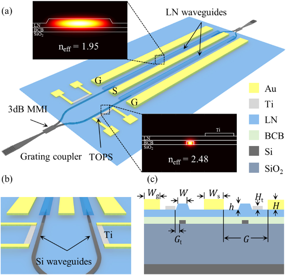
Figure 1.Schematics of the hybrid LN modulator with silicon TOPS. (a) Schematic of the whole structure. The insets are optical mode profiles of modulation and the TOPS region. (b) Perspective view of the TOPS. (c) Cross-section view of the high-speed modulation region and TOPS.
The silicon MMI split the input light into two optical paths that are isolated from one another. The thickness of the BCB bonding layer was set to 300 nm to provide a high coupling efficiency that promises that the optical power can be efficiently transferred to the LN layer through the vertical adiabatic couplers. To access the largest attainable EO coefficient of LN, the LN waveguides are formed along the axis of the LN membrane, while the gold electrodes create a horizontal electric field along the axis of LN. Consequently, the electric field has the opposite direction across the two waveguides, where the Pockels effect is used to induce an optical phase difference between them. To achieve high modulation efficiency and low optical loss, the fabricated waveguides have a top width of and a rib height of , and the gap between the waveguides and electrodes was set to 1.6 μm. The design of the TWE is optimized for impedance matching, low RF attenuation, and velocity matching to achieve higher EO bandwidth. Here, the thickness of the electrodes was set to , the widths of signal and ground electrodes were designed as and , respectively, while the gap between them was set to . Figure 2 shows the simulated and experimental results of the TWE parameters. After light coupling back from LN to silicon, TOPS can adjust the phase difference between the two arms via changing the applied voltage on the heating electrodes. The Ti electrodes are directly deposited on LN membranes after the etching process because LN has the characteristics of electrical isolation. The heating electrodes have a width of 2 μm, a height of , and a length of 160 μm. The device is compact due to the high TO coefficient of silicon ( at wavelengths near 1550 nm). To achieve a high TO modulation efficiency, the most important parameter is the gap between the waveguide and Ti electrode. A small gap can improve the heating efficiency but induce additional absorption losses. In this work, we focus on the demonstration of the combination of the TO bias controller with an EO modulator on one platform; thus, low optical loss is given priority under this situation. Here, the gap between the Ti heating electrodes and silicon waveguides under LN membranes was optimized to .
![]()
Figure 2.Simulated and experimental results of characteristic impedance
We fabricated silicon waveguides using standard electron beam lithography (EBL) and inductively coupled plasma reactive ion etching (ICP RIE). Then, a commercially available -cut LN-on-insulator (LNOI) die (NANOLN) was flip-chip bonded on the top surface of SOI substrate that was spin-coated with BCB. The whole sample is cured at a temperature of 270°C. Afterwards, the die handle of LNOI is removed by a series of processes consisting of mechanical polishing and dry/wet etching. Then, the pattern of LN waveguides was defined by EBL in hydrogen silsesquioxane (HSQ) resist, and the waveguides were formed by dry etching in an plasma. Finally, the Ti heating electrodes were deposited on the EBL-patterned polymethyl methacrylate (PMMA) resist patterned by electron beam evaporation, while the gold microwave transmission lines were produced in the same way. The scanning electron microscopy (SEM) images of the high-speed EO modulation region and TOPS are shown in Fig. 3.
![]()
Figure 3.Scanning electron microscopy (SEM) images of the modulator. (a) SEM image of the cross section of the high-speed modulation region. (b) SEM image of the cross section of TOPS. Both sections are formed by the focused ion beam (FIB) process.
3. RESULTS
The fabricated devices are characterized in detail. We first measured the optical transmission against the DC voltage applied on TOPS, as shown in Fig. 4(a). The results show of 1.83 V with the heating electrodes resistance of 696 Ω, which corresponds to the power dissipation required to achieve phase shift of 23.8 mW. This is more power-efficient compared to the minimum power consumption of 180 mW for the EOPS bias method, considering the 50 Ω terminator resistance. The on-chip loss of the modulator is measured to be 1.8 dB, which includes 1 dB LN and Si waveguides propagation losses, 0.4 dB vertical adiabatic coupler (VAC) coupling losses, and 0.4 dB from the two MMIs. In addition, the extinction ratio is measured to be approximately 40 dB for the device. Utilizing TOPS in silicon for bias control offers two distinct advantages compared to EOPS in LN. First, the TO effect of silicon is much stronger than the EO effect, allowing for a more compact size for TOPS. In our case, the length of the EOPS would have been more than 10 mm for the same amount of voltage. Second, LN is notorious for fast drifts in the bias point upon the application of a static electric field, which is a phenomenon that originates from the piezoelectric nature of the material. A fast feedback control loop to stabilize the bias point is normally required during the device operation of LN MZM. For TOPS in silicon, there is no such fast drift; hence, lower-speed, simpler control schemes can be used to compensate for device aging.
![]()
Figure 4.Experiments of the drift of the operating point for EOPS and TOPS bias control methods. (a) Transmission as a function of applied voltage on TOPS. (b) Power shift for TOPS and EOPS cases as a function of time. (c) Schematic of the experimental setup. The signals from the analog signal generator are set to 10 MHz. (d) Measured SHD intensity variations as a function of time. The red and blue curves correspond to the time-dependence change of SHD for TOPS and EOPS bias control, respectively. (e) Frequency response at the beginning of measurements for both two bias methods. (f), (g) Frequency response for the EOPS and TOPS bias control methods after operating for 2 h, respectively.
The bias point controlled by TOPS is stable and substantially free of DC bias drift. To demonstrate this, we first apply a DC bias to either TOPS or EOPS, such that the device is biased to a quadrature point with no modulation signal applied. We record the output power of the device for 60 min for both TOPS and EOPS, as depicted in Fig. 4(b). These results confirm that the DC bias point with the TOPS in silicon is much more stable than with the EOPS in LN. The little power drift for TOPS is caused by the instabilities of three-dimensional vertical coupling platforms. We then use the setup shown in Fig. 4(c) to interrogate the stability of the bias point with applied modulation signal. To provide a straight comparison towards the TOPS and EOPS bias methods, all of the measurements are performed on the same device. It is well known that the bias point of the MZM determines the level of nonlinear distortions in the modulated signal. Specifically, when applying sinusoidal modulation, the second-order harmonic distortion (SHD) terms in the modulated signal can be used as an indicator for the amount of DC drifts from the quadrature point, which can be explained by the following derivations. For an MZM, the output power in terms of the input power can be expressed as [31]
Finally, we performed detailed measurement in a data modulation experiment. Figure 5(a) shows the EO half-wave voltage measurement for the 9 mm long device with a 100 kHz triangular voltage sweep, and the measured is 3 V, corresponding to voltage-length product () of . The of the present device is a little larger than that reported in our previous work. Here, we sacrifice for better EO bandwidth and . As shown in Fig. 5(b), the 3 dB EO bandwidth of this device is greater than 67 GHz, which is beyond the measurement limits of our vector network analyzer (VNA). The ultra-high bandwidth means that the can be further decreased by simply increasing the modulation length while keeping an impressive bandwidth performance.
![]()
Figure 5.EO performance of hybrid Si and LN modulator. (a) Normalized optical transmissions as a function of the applied voltage on TWE. (b) EO bandwidth (
The high-speed transmission ability of the modulator has also been characterized. First, the OOK modulations were applied to the modulator. Figures 6(a) and 6(b) show the optical eye diagrams at 84 Gb/s and 100 Gb/s, and the measured extinction ratios are 7.2 and 5.9 dB, respectively. We also performed the PAM-4 modulation experiments at 53 Gbaud (106 Gb/s) and 64 Gbaud (128 Gb/s), and the results are shown in Figs. 6(c) and 6(d). Figure 6(e) shows the back to back (B2B) bit error rate (BER) versus the received optical power for 106 Gb/s and 128 Gb/s PAM-4 signal transmission. It should be worth noting that all of the bias control in the measurements is achieved by TOPS. In the measurements, a pre-amplified optical receiver consisting of a variable optical attenuator (VOA), an erbium-doped fiber amplifier (EDFA), a band-pass filter (BPF), and a 43 GHz PD was used. The output electrical signals were then sent to a 33 GHz real-time oscilloscope for analog-to-digital conversion and further digital signal processing (DSP). A feed-forward equalizer (FFE) with 31 taps was used to recover the PAM-4 signal. In addition to the data rate difference, the 2 dB power penalty between 53 Gbaud and 64 Gbaud is partly due to the bandwidth constraint of the oscilloscope.
![]()
Figure 6.High-speed transmission experiments. (a), (b) Optical eye diagrams for OOK signal at data rates of 84 Gb/s and 100 Gb/s. (c), (d) Measured PAM-4 modulation optical eye diagrams at 53 Gbaud (106 Gb/s) and 64 Gbaud (128 Gb/s). (e) Measured curves of BER versus the received optical power for 53 Gbaud (106 Gb/s) and 64 Gbaud (128 Gb/s) PAM-4 signals.
4. CONCLUSION
As presented above, the heterogeneous LN/SOI MZM demonstrated here can achieve excellent optical modulation characteristics, featuring stable and substantially free of DC bias drift phenomena. We note that the long-term (months) stability of the device should be studied in the future. LN phase modulation waveguides and TOPS can be fabricated with lithographic precision and alignment accuracy in a back-end process after the SOI fabrication. This manufacturing procedure is highly scalable. As pure phase modulation capability in a SiPh platform can only be achieved by utilizing slow TO effects, while carrier effects allow high-speed phase modulation accompanied by phase-dependent loss, the approach demonstrated here allows for the combination of both slow and fast pure phase modulation capabilities in the SiPh platform. Therefore, our approach potentially provides a new generation of compact, high-performance, and very stable optical modulators for telecommunications and data interconnects, as well as opens up new avenues for many new applications, such as quantum photonics and microwave photonics, where pure phase modulation is crucial.
Acknowledgment
Acknowledgment. X. Cai thanks Dr. P. Jiang for insightful discussion.

Set citation alerts for the article
Please enter your email address
© Copyright 2018-2021 | Chinese Laser Press. All Rights Reserved 沪ICP备15018463号-20