1Key Laboratory of Optoelectronic Information and Sensing Technologies of Guangdong Higher Education Institutes, Department of Optoelectronic Engineering, Jinan University, Guangzhou 510632, China
2Engineering Research Center on Visible Light Communication of Guangdong Province, Department of Optoelectronic Engineering, Jinan University, Guangzhou 510632, China
3Key Laboratory of Visible Light Communications of Guangzhou, Jinan University, Guangzhou 510632, China
4Science and Technology on Reliability Physics and Application of Electronic Component Laboratory, China Electronic Product Reliability and Environmental Testing Research Institute, Guangzhou 510610, China
In graphene-based optoelectronic devices, the ultraweak interaction between a light and monolayer graphene leads to low optical absorption and low responsivity for the photodetectors and relative high half-wave voltage for the phase modulator. Here, an integration of the monolayer graphene onto the side-polished optical fiber is demonstrated, which is capable of providing a cost-effective strategy to enhance the light–graphene interaction, allowing us to obtain a highly efficient optical absorption in graphene and achieve multifunctions: photodetection and optical phase modulation. As a photodetector, the device has ultrahigh responsivity () and high external quantum efficiency (). Additionally, the polybutadiene/polymethyl methacrylate (PMMA) film on the graphene can render the device an optical phase modulator through the large thermo-optic effect of the PMMA. As a phase modulator, the device has a relatively low half-wave voltage of 3 V with a 16 dB extinction ratio in Mach–Zehnder interferometer configuration.
1. INTRODUCTION
Nowadays, optoelectronic devices are moving towards miniaturization and integration. On-chip optical interconnects, especially silicon photonics, provide a promising platform for miniaturized optoelectronic integration [1]. However, it is usually required to couple the silicon photonic devices with optical fibers for the photonic signal transmission. The mode-mismatch and the large index difference between the silicon waveguide (width μ, 3.42) and single-mode fiber (core diameter μ, 1.463) lead to a relatively high coupling loss [2]. The incompatibility of material characteristics and processing technology of silicon and optical fiber requires long assembly time and high cost to achieve accurate coupling [3]. The integration of an optoelectronic device onto optical fiber is potentially expected to solve the issue of incompatibility between chip and optical fiber. The fiber-integrated optoelectronic devices, such as an fiber end face-integrated photodetector based on -graphene [4], an electro-optic modulator by growing graphene on photonic crystal fiber (PCF) [5], and all-optical modulator based on graphene-clad microfiber [6], are compatible with current fiber-optic networks. However, the microfiber suffers from poor mechanical properties; the grown of graphene–PCF needs precise control and it is difficult to fabricate electrodes on the curved fiber surface. The side-polished fiber (SPF), usually polished by a single-mode fiber, has the natural advantage of seamless connecting with the current optical fiber system, has reliable mechanical properties, and the polished surface provides a flat platform for device integration. The strength of evanescent field interaction with matter is determined by the distance from the polished surface to the fiber core [7], and the long side-polished region () helps to strengthen the light–matter interaction.
It is a very challenging task to integrate multifunctions into one device because different functions are generally based on different mechanisms, materials, and structures [8]. However, the emergence of two-dimensional (2D) materials sheds substantial light on multifunctional devices [9–12]. In 2016, an optoelectronic device based on vertical heterojunction was fabricated with the functionalities of both photodetection and light emission [9]. The photodetection and programmable charge storage have been integrated into a graphene- hybrid device [10]. The graphene-based silicon waveguide can be used for both optical modulation and photodetection [11]. But there is little research on integrating multifunctions in an optical fiber. Our group has demonstrated a graphene multifunctional device with electro-optical modulation and photodetection based on coreless side-polished fiber (CSPF), which, however, suffers from low photoresponsivity and specific modulation wavelength [12]. What is more, the electrodes of the device are not integrated onto the fiber but onto the glass substrate, so it is not really an all-fiber device. Photodetectors and modulators are indispensable devices in photonic systems [13]. The commercial photodetectors are generally based on semiconductors such as Si, Ge, and InGaAs, and the phase modulators are generally based on a crystal. Restricted by the incompatible material characteristics and processing technology of semiconductor and crystal, to date, there is no device that can integrate a photodetector and phase modulator into one device. The “half-wave” voltage can be used to describe the modulation capacity of an electro-optic phase modulator that makes [14], and the is 3–5 V in commercial devices [15]. With the development of 2D materials, electro-optic graphene-based phase modulators have been proved to be effective in silicon waveguides, but they suffer from large optical losses () [16–19]. Therefore, integration of graphene with SPF is expected to achieve low transmission loss phase modulators and high-performance photodetectors. Implementing a high-performance multifunction device can make the integrated optical system adaptable and meet the needs of the coming fifth-generation (5G) era.
Graphene, due to its excellent optical and electronic properties, holds great prospects for broadband and ultrafast optoelectronic devices, and its flexibility makes all-fiber integration possible. Different kinds of graphene-based optoelectronic devices have been demonstrated, ranging from optical polarizer [20], modulator [21,22], and switch [23], to photodetector [24,25]. However, pure monolayer graphene photodetectors suffer from low photoresponsivity, while the photoresponsivity does not exceed 32 A/W [12,24,26–32]. The two major restrictions for the low photoresponsivity are the low optical absorption () and short photocarrier lifetime of monolayer graphene [23,33]. Significantly improving the responsivity of pure graphene photodetectors is a prerequisite for their widespread application [34]. Some attempts have been adopted to improve the photoresponsivity of the graphene photodetector, including modifying graphene with quantum dots [35,36], microcavities [37], and surface plasmons [38–40]. Although these attempts can improve responsiveness, the introduction of quantum dots will prolong the response time, the microcavity will restrict the wavelength bandwidth, and surface plasmons will increase absorption loss. Hence, developing pure graphene photodetectors has the potential to achieve a broadband and high-speed detection, and the top priority is to find a way to achieve high responsivity.
Sign up for Photonics Research TOC. Get the latest issue of Photonics Research delivered right to you!Sign up now
In this paper, we demonstrate a multifunctional device that can work at room temperature by integrating a hybrid graphene/polybutadiene (PB)/polymethyl methacrylate (PMMA) film onto an SPF. There is no need to dope graphene and compound other materials; the extra-long side-polished region and the high refractive index PMMA work together to enhance the light and graphene interaction, resulting in ultrahigh responsivity over a broadband range of 980 to 1610 nm in a low cost and efficient way. At 1550 nm, the all-fiber graphene device (AFGD) possesses a responsivity of and a response time of , although the carrier mobility of graphene we used is just . The influence of residual thickness of the SPF is investigated in detail. With the assistance of the thermo-optic effect of PMMA, the AFGD can work as an optical phase modulator. Based on the Mach–Zehnder interferometer (MZI) configuration, a maximum phase shift of is obtained at a bias voltage of 6 V with an extinction ratio up to 16 dB; the half-wave voltage is 3 V. What is more, in order to improve the air stability of graphene, we added the PB layer to protect graphene against water and impurity. This simple, high-performance, and easy-to-integrate multifunction device provides a reliable way to realize photon transport, detection, and phase modulation in a single optical fiber.
2. RESULTS AND DISCUSSION
A. Fabrication
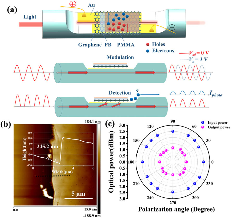
The structure of the AFGD is shown in Fig. 1(a). The whole device is integrated onto the side-polished region of the SPF. By wheel side-polishing technique, a single-mode fiber (SMF-28e) is polished into an SPF with a D-shaped cross section by removing part of the optical fiber [41]. The single-mode fiber has a core diameter of 8 μm and a cladding diameter of 125 μm. In order to protect graphene and improve the stability of AFGD, we spin-coat a thin PB layer on chemical vapor deposited (CVD)-grown graphene before coating the PMMA film. The nonpolar PB layer effectively prevents Fermi-level change in the graphene [42] and reduces the charged impurity scattering from a polar adjacent layer or the residue of PMMA small molecules [43]. After etching Cu foil, a narrow strip of hybrid graphene/PB/PMMA film is wet-transferred onto the side-polished region of the SPF. Before that, we prepare a 50 nm Au film by physical vapor deposition on the SPF and scrape a gap of μ in the middle of the Au film with a needle to expose the fiber core. Thus, the fiber mode can leak out and interact with the graphene/PB/PMMA film. The as-fabricated Au microstrip electrodes (length , width μ) are placed on the side-polished region. Figure 1(b) shows the AFM image of hybrid graphene/PB/PMMA film, indicating that the thickness of the hybrid film is . The AFM image of graphene/PMMA film without PB is shown by Fig. 9 in Appendix A, from which one can derive the thickness of PMMA as . Thus, the thickness of the PB layer is estimated as .
Figure 1.(a) Schematic of optic-phase modulation and photoelectric detection by the AFGD, where two microstrip electrodes are fabricated on an SPF deposited with a hybrid graphene/PB/PMMA film; (b) atomic force microscopy (AFM) image of hybrid graphene/PB/PMMA film. The inset shows the cross sections of graphene/PB/PMMA film, indicating the thickness of the film being 245.2 nm. (c) The input (pink spheres) and output (blue spheres) optical power of AFGD changing with the incident polarization angle.
The input and output optical power of AFGD changing with the incident linear polarization angle is shown in Fig. 1(c).When the input power is 2.5 dBm, which is larger than the saturation power, the output power is independent of polarization due to the saturation absorption of graphene. The output power through the AFGD is , with a total loss low to 1.4 dB. The output power changes 16% when the polarization angle increases from 0° to 360°. Hence, our device is polarization-insensitive. The polarization insensitivity should be caused by the same absorption of TE and TM by graphene under the saturation input power.
The eigenmodes of graphene-coated SPF with and without the PB/PMMA film are analyzed by the commercial finite element software COMSOL Multiphysics. Owing to the thin thickness of the dielectric PB (), we regard hybrid PB/PMMA film as a whole with an effective refractive index of (, , thickness ratio 1:5) in the simulation [44,45]. The simulated results are shown in Fig. 2(a). Without the hybrid film, the normalized field intensity at the graphene location is 0.086. With the aid of PB/PMMA film, the fiber mode is dragged from the fiber core, and the normalized field intensity increases to 0.185 at the graphene location, with an enhancement factor of 2.15. Therefore, the absorption of graphene-coated SPF with and without PB/PMMA film should be different.
Figure 2.(a) Normalized intensities along the axis for the cases with and without PB/PMMA. Insets show the enlarged TE mode intensity distribution at position of graphene. (b) Transmission spectra of bare SPF (pink line), SPF covered with graphene (blue line), and SPF covered with hybrid graphene/PB/PMMA film (red line).
Figure 2(b) compares the transmission spectra of the SPF covered with graphene and graphene/PB/PMMA film. The light absorption possesses a dip around 1500 nm, which comes from the multimode interference effect in the SPF [46]. The light absorption is greatly enhanced over the whole bandwidth ranging from 900 to 1600 nm, when a hybrid PB/PMMA film is placed over the graphene-coated SPF.
B. Photodetection
For characterizing the photoresponse of the AFGD, a 1550 nm light from a tunable laser passes sequentially through a variable optical attenuator, polarization controller, and coupler. A 50:50 optical fiber coupler splits the optical power into two parts: one part is injected into an optical power meter directly for power monitoring; the other is into the AFGD. The generated photocurrent is measured by a digital source meter.
Figures 3(a)–3(d) show the measured photocurrents and photoresponsivities under different illumination intensities. As shown by Fig. 3(a), the photocurrents () increase linearly with the bias voltage () for different light powers; this linear relationship between photocurrent and indicates that the ohmic contact between the graphene and Au electrode is good. When the bias voltage is zero, no photocurrent can be found. As shown in Fig. 3(b), the photocurrent varies with the incident light power; the AFGD possesses the ability of femtowatt-level optical power detection. The photocurrent below 0.275 nW can be fitted by power law . Compared to the ideal factor 1, the fitting factor 0.83 implies that there are some trap states existing in the bandgap [26,47]. The trap states may come from the contaminations of etchant solution and residual Cu during the wet-transfer process of CVD-grown graphene [48]. The residual impurity can trap the free electrons from graphene to prolong the lifetime of the trapped carriers and improve the responsivity [49]. The photocurrent increases rapidly with the incident power at the beginning, and then varies much slower after 0.275 nW. Thus, 0.275 nW can be considered as the saturation power. This result is comparable to those previously obtained by graphene photodetectors [50,51]. The linear dynamic range (LDR) is used to characterize the application range of the light intensity detected by the photodetector. It is given by , where is the saturation power (0.275 nW). The minimum detectable optical power is determined by the noise equivalent power (NEP) and the measurement bandwidth [52]. As will be shown below, the NEP decreases with the modulation frequency. The NEP is at 1 Hz [51,53]. Thus, can be estimated as 1.4 fW for . As calculated from the photocurrent versus incident light power curve, the theoretical LDR of AFGD is 106 dB. Figures 3(c) and 3(d) show the responsivity (defined as ) of the AFGD as functions of the bias voltage and light power, respectively. For a weak incident light (the incident light power is lower than the saturation power), the responsibility keeps almost unchanged. When saturation absorption occurs, the concentration of carriers inside graphene no longer increases. The photocurrent barely increases, while the corresponding responsivity starts to decrease. There is a linear relationship between the responsivity and incident light power in log-log coordinates.
Figure 3.(a) Photocurrent and (c) responsivity of the AFGD as a function of bias voltage for different light powers at 1550 nm; (b) photocurrent and (d) responsivity of the AFGD changing with the light power at , where both axes are in the logarithmic scale; (b) shows a broad LDR of AFGD in weak light. (e) Schematic of electron–hole pair excitation in graphene for weak light; (f) schematic of graphene saturated absorption; (g) polarization-independent property of the generated photocurrent of the AFGD for 1550 nm incident light (, ).
We achieved a strong light–matter interaction due to the PMMA layer and long interaction length (); a maximum responsivity up to is achieved when the light power is 69 pW and the bias voltage is 0.3 V. As shown in Fig. 3(e), when weak light is absorbed by graphene, interband transition of carriers will occur [54]. However, when the incident power increases, the conduction and valence bands will be fully filled by the photogenerated carriers, blocking further absorption, as shown by Fig. 3(f). In this case, the photocurrent will keep, and the responsivity begins to decrease. Figure 3(g) shows the photocurrent as a function of the linear polarization angle under a saturation incident power. The polarization is controlled by a fiber bench manual polarization controller. By rotating the polarization controller in a circle, the photocurrent variation is smaller than 15%. Thus, one can conclude that the photoresponse of this device is polarization-insensitive. In some specific applications, such as spectroscopic detection and phase imaging [55], polarization-insensitive devices are more appealing.
The AFGD is broadband and stable. Figure 4 shows the photocurrent and responsivity of the AFGD for wavelengths ranging from 980 to 1610 nm. The broadband responsivity can accurately illustrate the performance of the device [56]; the is larger than under 1 nW illuminated at 980–1610 nm. The residual thickness of the SPF plays an important role in light absorption—thus the responsivity of the AFGD. Figure 4(c) shows the responsivity changing with the residual thickness. The maximum responsivity is found at the residual thickness of 66.5 μm, which is up to . The refractive index of the hybrid PB/PMMA film is higher than that of the fiber core; thus the film can drag the evanescent field out of the fiber core. The PB/PMMA can be considered as an asymmetric cavity, which greatly enhances the light absorption of the monolayer graphene from 2.3% to 65.53% by simulation, as shown in Fig. 4(d). The light absorption of the whole device can be calculated by: , where is the length of the hybrid film, and is the imaginary part of the effective refractive index fundamental modes at . The absorption is increased from 2.1% to 65.4% when the residual thickness changes from 60.5 to 64.5 μm, and the corresponding responsivity is increased from 42 A/Wto . This giant responsivity improvement comes from the absorption enhancement and the carrier multiplication effect in graphene [57]. With the PB/PMMA film protecting the monolayer graphene, our devices can maintain long-lasting stable photodetection over 6 months in the air. From Fig. 5, the decline of the photocurrent and responsivity is smaller than 10% after 6 months at 1550 nm ().
Figure 4.(a) Photocurrent and (b) responsivity of the AFGD as a function of light power at 980 nm (red lines), 1310 nm (pink lines), 1550 nm (green lines), and 1610 nm (blue lines) at residual thickness of 68 μm (); (c) responsivity changing with the residual thickness at 1550 nm (, ); (d) simulated absorption changing with the residual thickness. The insets in (c) show the macroscopic images of the cross section of SPFs. The insets in (d) show the intensity distributions of the fiber modes of SPFs.
Figure 5.Air stability characterization. (a) The photocurrent and (b) responsivity tested as fabricated and 6 months later, at 1550 nm at room temperature ().
By measuring the noise in the dark current (see Fig. 6), the ability of the AFGD to detect weak light has been characterized. The noise may come from the shot noise and thermal noise of the AFGD as well as the flicker noise of the electronic equipment. The frequency-dependent noise spectral density of the photodetector is given under 0.3 V bias voltage. The noise spectral density decreases with the modulation frequency. The NEP is found to be at 1 Hz, with . The specific detectivity is defined as , where is the effective area of the photodetector, estimated as μ. Thus, is Jones.
Figure 6.(a) Dark current waveform of the AFGD with the source-drain voltage of and the sampling frequency of 1.8 kHz; (b) analysis of noise spectral density of the AFGD based on the dark current waveform measured in (a).
Finally, the dynamic response of the AFGD is investigated. Figure 7(a) shows the photocurrent over an eight-period on–off operation at 1550 nm. The incident light signal is a 1 Hz square-modulated 1550 nm laser with a power of 10 dBm. Under the protection of the PB layer, the photocurrent is stable and well repeatable. From Fig. 7(b), the rise time can be estimated as 93 ms, which is determined by the electric signal rising time interval from 10% to 90% of saturated value [58]; the decay time is 98 ms. Compared with both the responsivity and bandwidth of other pure monolayer graphene photodetectors [see Fig. 7(c)], our AFGD shows an unprecedented responsivity. Although this device is capable of achieving ultrahigh responsivity in this particular structure, the low carrier mobility () and long lifetime of the trapped carriers (49 ms) restrain its operation bandwidth. The carrier mobility of is measured using a reference structure (see Fig. 10 in Appendix A2). It is a challenge to achieve high sensitivity and fast operating speed simultaneously for photodetectors. The gain-bandwidth product is an important parameter for any amplification mechanism in photodetectors [59].
Figure 7.(a) Time-dependent photocurrent over eight-period on–off operation at 1550 nm; (b) the enlarged view of photocurrent shows the response time is (). (c) Comparison of the responsivity and operation speed for the AFGD with some of the high-performance pure graphene photodetectors reported in the literature [12,24,26–32" target="_self" style="display: inline;">–32]; (d) exponential attenuation of the photocurrent when there is no optical signal.
Here, we get the AFGD with a gain-bandwidth product of 0.34 GHz, where the photoconductive gain is about (see Appendix B). The large gain leads to the external quantum efficiency (EQE) as high as , and the incident photon-to-electron conversion efficiency (IPCE) can be calculated by . Using IPCE to describe the photoelectric conversion efficiency of the photodetector is more accurate because it takes into account both the photo-to-electron conversion of absorbed light and the light absorption. Compared with the graphene photodetector based on () [24], our device has greatly enhanced the IPCE by a long photon–matter interaction length (6 mm) and a highly efficient optical absorption (65.53%) in light absorption. Compared with the graphene photodetector based on () [24], our device has greatly enhanced the IPCE by a long photon–matter interaction length (6 mm) and a highly efficient optical absorption (65.53%) in graphene [60]. Figure 7(d) shows the lifetime of the trapped carriers , which is equal to the time it takes for the nonequilibrium carrier concentration to decrease to 1/e of the original value. And the photocurrent of transient measurement when switching the light off can be fitted by an exponential decay function of [61]. The long carrier lifetime is a benefit for large gains, but it sacrifices switching speed. Table 1 lists the performance of the AFGD compared with other fiber-optic waveguide-based photodetectors reported in the literature. Unlike Si- or -based photodetectors, fiber-based photodetectors generally have longer response time, while our work has shown advantages in responsivity and detectivity.
Waveguide
Material
Detectivity (Jones)
Response Time
Wavelength
Responsivity
NEP (W·Hz−1/2)
References
Microfiber
Graphene
1500–1600 nm
2.81 mA/W
1×10⁻⁹
[6]
CSPF
Graphene
81 ms, 77 ms
Near-infrared
0.44 A/W
[12]
Fiber end face
CsPbBr3-graphene
8.6×10¹⁰
3.1 s, 24.2 s
400 nm
2×10⁴ A/W
3.9×10⁻¹⁶
[4]
SPF
Graphene
3.29×10¹¹
93 ms, 98 ms
980–1610 nm
1.5×10⁷ A/W
1.4×10⁻¹⁵
This work
Table 1. Comparison of the Performance of the Fiber Waveguide Photodetectors
According to the theory of Prud’homme, the thermal-optic coefficient of PMMA can be expressed as , where is the refractive index of the PMMA, is the temperature coefficient of the electronic polarizability, and is the coefficient of thermal expansion [15]. For the temperature of PMMA film increasing 1°C, its refractive index will decrease by , resulting in a decrease in the effective refractive index of the fiber mode. Therefore, except for photodetection, this device can also be applied for phase modulation by thermo-optic effect of PMMA by controlling the applied bias voltage.
To demonstrate the all-fiber graphene phase modulation, we design an MZI system as shown in Fig. 8(a). Two 3 dB optical couplers are used as the input splitter and the output combiner, respectively. In order to equalize the optical power of the two arms, a variable optical attenuator is added to the optical path of the reference arm. The AFGD is inserted into the signal arm with a bias voltage applied by a digital source meter (Keithley 2450). When a bias voltage is applied on the AFGD, the electric current will heat the monolayer graphene due to ohmic heating. Owing to the high thermal conductivity of graphene, heat will transfer to PMMA film quickly, inducing its change in the refractive index.
Figure 8.(a) Experimental setup of the MZI-based graphene phase modulator. OC1 and OC2, 50:50 optical fiber coupler; VOA, variable optical attenuator. (b) Interferometric spectra at output 1 for the bias voltage being 0 V (blue dashed line) and 6 V (red solid line); (c) phase shift and temperature rise versus the bias voltage; (d) transmission power varies with a square bias voltage signal; in situ infrared thermograms of AFGD at (e) 0 V and (f) 5 V.
The phase shift of light in the PMMA film is , where is the length of hybrid film. As the fiber mode in SPF evanescent-couples to the PMMA film, the optical phase of the fiber mode will shift accordingly. Thus, the interferometric spectra at output 1 will shift when a bias voltage is applied. As shown in Fig. 8(b), the blue curve shows no phase shift interference spectrum without applied voltage. When the bias voltage is increased to 6 V, the interference spectrum shifts towards the long wavelength for about 0.052 nm (red curve), corresponding to a phase shift of (). The free spectral range (FSR) is about 0.034 nm. From Fig. 8(c), is estimated as 3 V, which is comparable to the commercial devices () [15]. The modulation efficiency of this phase shifter can be calculated by (1.8 V · cm) [62], where is the length of the phase shifter, estimated as 6 mm. The AFGD possessed an extinction ratio of 16 dB in MZI configuration. The relation of phase shift to bias voltage and temperature rise is shown in Fig. 8(c). A maximal phase shift of was obtained at a bias voltage of 6 V; the corresponding temperature rise is 1.6°C. We also measured the modulation of transmission power under a square voltage signal between 0 and 5 V. The transmission power shows good repeatability. The AFGD temperature is in situ monitored using a thermal imaging camera (Fotric). As shown in Figs. 8(e) and 8(f), the maximum temperature without an applied bias voltage is 29°C, and the maximum temperature rises to 30°C when a 5 V bias is applied. This modulator is expected to encode electronic data signals into optical fibers.
3. CONCLUSIONS
In summary, we have fabricated a polarization-insensitive multifunctional graphene-optoelectronic device on SPF with low insertion loss, which can realize both photoelectric detection and optic-phase modulation. By this particular structure, we improve the optical absorption of monolayer graphene to 65.53%. This photodetector has a wavelength-dependent photoresponse with responsivity of and a high gain-bandwidth product of 0.34 GHz. High responsivities are achieved over a broadband region of 980–1610 nm, and the AFGD shows a broad LDR of 106 dB in weak light. As an all-fiber phase modulator, the half-wave voltage is 3 V, and the maximal phase shift can reach when the bias voltage is 6 V. The extinction ratio can reach 16 dB based on MZI configuration. And with the protection of the PB layer, our device can work stably in the air environment for about half a year. This work not only paves the way to realize a multifunctional fiber-integrated optoelectronic device, but also provides a novel solution to break the device limitation due to the ultraweak interaction between light and 2D materials.
Acknowledgment
Acknowledgment. The authors would like to thank Prof. Rihui Yao for providing us with the instrument for physical vapor deposition of Au film.
APPENDIX A: CHARACTERIZATION OF GRAPHENE
AFM Image of Graphene/PMMA Film
The AFM image of the graphene/PMMA film is shown in Fig.?9.
Figure 9.(a) AFM image of graphene/PMMA film; (b) cross section of graphene/PMMA film from the dashed line shown in AFM image; the thickness of the film is 203.6 nm.
The photoconductive gain can be given by [63] where is the lifetime of the trapped carriers, is the drift transit time, is the separation distance of source-drain, is the dielectric constant of the medium between electric fields, is the applied voltage of source drain, is the graphene’s hole mobility, and is the electronic mobility. Among them, μ, , and . For simplicity, we assume that the electric field is uniform and in a vacuum (), so and .