1College of Physics and Optoelectronics, Key Laboratory of Advanced Transducers and Intelligent Control System of Ministry of Education, Key Laboratory of Interface Science and Engineering in Advanced Materials of Ministry of Education, Taiyuan University of Technology, Taiyuan 030024, China
2Key Laboratory of Applied Surface and Colloid Chemistry, MOE; Shaanxi Key Laboratory for Advanced Energy Devices; Shaanxi Engineering Laboratory for Advanced Energy Technology, School of Materials Science and Engineering, Shaanxi Normal University, Xi’an 710119, China
3Dalian National Laboratory for Clean Energy; iChEM, Dalian Institute of Chemical Physics, Chinese Academy of Sciences, Dalian 116023, China
4University of Chinese Academy of Sciences, Beijing 100049, China
Solution-processable, single-crystalline perovskite nanowires are ideal candidates for developing low-cost photodetectors, but their detectivities are limited due to a high level of unintentional defects. Through the surface-initiated solution-growth method, we fabricated high-quality, single-crystalline, defects-suppressed nanowires, which possess atomically smooth side surfaces with a surface roughness of 0.27 nm, corresponding to a carrier lifetime of 112.9 ns. By forming ohmic contacts through the dry contact method, high-performance metal–semiconductor–metal photodetectors have been demonstrated with a record large linear dynamic range of 157 dB along with a record high detectivity of at an illumination power density of . Such superior photodetector performance metrics are attributed to, first, the defects-suppressed property of the as-grown nanowires, which leads to a quite low noise current in the dark, and second, the ohmic contact between and Au interfaces, which gives rise to an improved responsivity compared with the Schottky contact counterpart. The realized high-performance nanowire photodetector advances the development of low-cost photodetectors and has potential applications in weak-signal photodetection.
1. INTRODUCTION
The emerging organic–inorganic hybrid perovskites, being regarded as one of the most promising semiconductor materials, appear to possess advantages of both inorganic and organic semiconductors [1–9]. The hybrid components enable the perovskites to exhibit excellent electronic characteristics, such as high carrier mobility, long carrier lifetime, and low trap density, just like inorganic semiconductors [10–12]. In addition, hybrid perovskite semiconductors also display such features as adjustable bandgap and low-temperature processing, similar to their organic counterparts [13–17]. Ascribed to the unique features of hybridization, perovskites have already shown bright prospects in the fields of solar cells [18–27], light-emitting diodes (LEDs) [28–31], and lasers [32–35]. Along the same lines, research on perovskite photodetectors has also attracted widespread interest [2,36–40]. Various perovskites photodetectors including single-crystal, thin-film [41–46], and quantum dot [47–52] perovskite photodetectors have been successfully demonstrated. The figure of merit that characterizes a photodetector’s ability to detect weak-light irradiation is the specific detectivity (). Only high-quality semiconductor crystals can suppress the dark current, resulting in high- photodetection performances.
Perovskite photodetectors can be categorized into different groups according to the crystalline properties of the perovskite layer. Generally, single-crystalline perovskite bulk material, wafers, and films are superior to their polycrystalline counterparts in terms of lower carrier recombination loss and longer carrier lifetime because of a reduced density of grain boundaries and defects. Therefore, single-crystalline-based perovskite photodetectors show advantages of lower dark current, promoting the as well as the linear dynamic range (LDR), which is crucial for weak-signal photodetection [53–58]. Differing from the frequently investigated bulk materials or wafers, low-dimensional perovskite nanostructures such as nanowires and nanoplatelets allow the manipulation of light at the nanoscale via naturally formed boundaries [59–62], and they also meet the need for good flexibility [63–69]. A series of different solution-processing techniques has been applied for preparing single-crystalline perovskite nanowires, based on which high-performance photodetectors have been demonstrated [63,64,67–80]. In 2016, by the blade-coating method, Jie’s group achieved ordered wires of the micrometer scale and demonstrated photodetectors with a of [67]. Later, they demonstrated a type of nanowire photodetector with wires grown via the saturated-vapor-assisted solution-growth method, and obtained a of [76].
Although the state-of-the-art nanowire photodetectors have achieved tremendous success, most reported nanowires show obvious morphological imperfections, e.g., rough surface [67,69,81] and irregular facets [64,73,76], associated with unintentional surface defects. It is expected that these surface defects will certainly induce inevitable carrier recombination loss and unfavorable scattering loss, shortening the carrier lifetime as well as deteriorating the dark current. It is apparent that reducing the density of surface defects in the perovskite crystal is a promising route to lower the dark current and promote the specific of perovskite photodetectors [1]. With this aim, Tang et al. immersed the solution-grown nanowires in oleic acid, bringing forward a reduced dark current as well as an increased response under illumination, so that the was improved by an order of magnitude (reaching ), and the corresponding LDR reached 140 dB, which is the largest reported [73]. It is noticed that Song et al. proposed a so-called surface-initiated solution-growth strategy to produce single-crystalline nanowires [16,60,82], which could act as high-performance laser cavities with a quality factor as high as 3600, outperforming all the other reported nanocavities [83–86]. The surfaces of their nanowire products displayed an RMS roughness value as low as 4 nm, corresponding to a relatively low density of surface defects. It is expected that this type of nanowire with fewer surface defects may serve as a promising platform for developing photodetectors with high .
Sign up for Photonics Research TOC. Get the latest issue of Photonics Research delivered right to you!Sign up now
In this work, based on the surface-initiated solution-growth strategy, we produced high-quality, single-crystalline nanowires with a carrier lifetime as long as 112.9 ns, which is around twice that of oleic acid passivated nanowires (51.1 ns) [73]. The atomic force microscopy (AFM) characterization indicates that the produced nanowires display atomically smooth surfaces with an RMS roughness down to 0.27 nm, an order of magnitude lower than the best result in the literature [60]. Such a smooth morphology of the as-grown nanowires indicates significantly minimized surface defects, accounting for the obtained long carrier lifetime. Through a dry-contact technique, we realize ohmic contacts between nanowires and Au electrodes, and further demonstrate high-performance photodetectors that can respond linearly to illumination with the power density varying from to , corresponding to an LDR as large as 157 dB. At the lowest detectable illumination () of , its responsivity () is as high as , and its derived from the measured noise current reaches . To the best of our knowledge, our photodetector presents both the largest LDR and the highest among all nanowire photodetector devices. Such superior photodetector performance metrics are attributed to, first, the defects-suppressed property of the as-grown nanowires, which leads to a quite low noise current in the dark, and second, the ohmic contact between and Au interfaces, which gives rise to an improved compared with the Schottky contact counterpart. Our work contributes to the development of high-performance, next-generation, low-cost photodetectors.
2. RESULTS AND DISCUSSION
The single-crystalline nanowires are grown by the optimized surface-initiated solution-growth strategy as shown in Fig. 5 (Appendix A). When the coated transparent lead acetate () solid film is immersed into the methyl ammonium iodide (MAI) solution, the film immediately turns brown, due to the production of a thin layer of polycrystalline on its surface. This layer serves as a seed layer to initiate the crystal growth; hence, the strategy is referred to as the “surface-initiated solution-growth” strategy. After the reaction is finished, the product of the single-crystalline nanowires is harvested with an additional process of isopropanol (IPA) wash for removing the residual MAI. Our previous work concluded that the length and amount of the produced nanowires can be well controlled by the precursor concentration and the growth temperature [87]. In this work, we also investigate the influence of environmental humidity on the reaction and find that a humidity of is the optimal condition for obtaining the nanowire products with the highest density and best crystallinity, as shown in Fig. 6 (Appendix B). Because IPA can take up moisture from air due to its hygroscopic property, we suspect that water molecules can interact with the polycrystalline perovskite surface and localize electrons close to its surface [88], which might act as a driving force for initiating the growth of the nanowires. With the increase in humidity from 20% to 30%, there would be more water molecules in the IPA solution, resulting in more sites with localized electrons at the polycrystalline perovskite surface, thereby producing more nanowires. In comparison, at a high level of humidity (e.g., 35%), water molecules interact with each other and form a hydrogen bonded network [88]. Thus the localization of electrons at the polycrystalline perovskite surface cannot be produced efficiently, which means the favorable factor for initiating the growth of nanowires is weakened. As a result, the density of the nanowire product decreases at a high humidity of 35%.
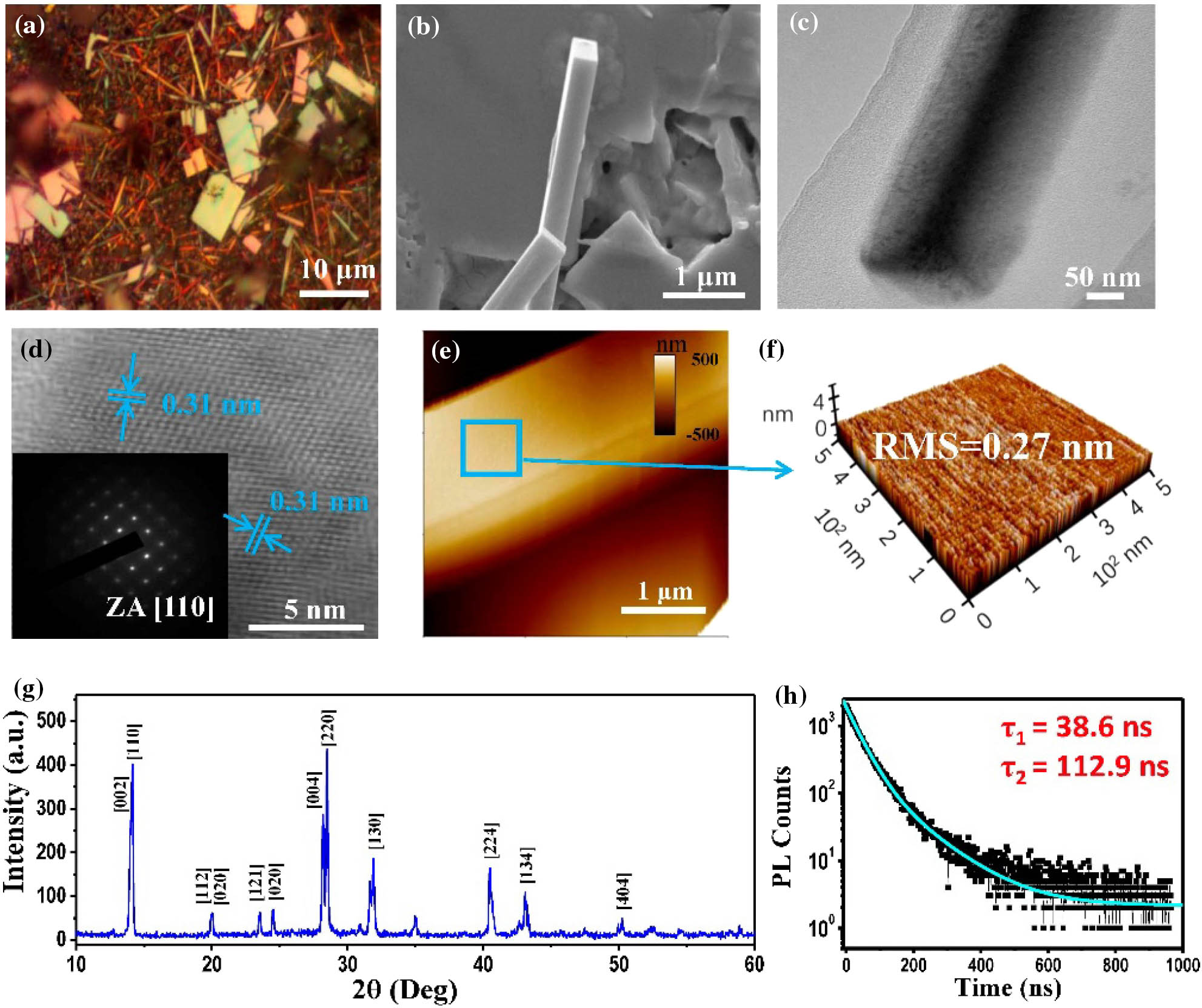
Figure 1(a) presents a typical optical image of the as-grown nanowires accompanied by a few nanoplatelets on a glass substrate. It can be seen that the prepared perovskite nanowires are rich in color because the thicknesses of the nanowires are different, and interference occurs between the beams reflected from the top and bottom surfaces of the nanowires [89]. These nanowires have flat rectangular end facets with dimensions of a few hundred nanometers as indicated by the scanning electron microscopy (SEM) images in Fig. 1(b). The transmission electron microscopy (TEM) analysis of a single nanowire was carried out as displayed in Fig. 1(c). A high-resolution TEM image of a single nanowire with the spacing of the lattice fringes measured to be is shown in Fig. 1(d), and the fringes are indexed as (004) or (220) of the tetragonal phase [73]. The inset of Fig. 1(d) presents the corresponding selected-area electron diffraction and fast Fourier transform (FFT) patterns. The sharp diffraction spots indicate that the synthesized nanowire has a tetragonal crystal structure with zone axes of [110] or [001].
Figure 1.(a) Optical image of nanostructures grown from thin film. (b) Cross-sectional SEM image of a single nanowire. (c) Low-resolution TEM image of a single nanowire. (d) High-resolution TEM image of a selected area of a single nanowire; the inset represents its corresponding FFT pattern. (e) AFM image of a single nanowire. (f) AFM image of the selected nanowire region with the average surface roughness measured to be 0.27 nm. (g) XRD pattern of as-grown nanowires with a comparison of the simulated tetragonal phase . (h) Transient PL spectrum of the nanowire.
The X-ray diffraction (XRD) patterns of the prepared nanowire are characterized as shown in Fig. 1(g), in good agreement with the corresponding simulated tetragonal-phase XRD pattern shown in Fig. 7 (Appendix B). Apparently, the pattern shows multiple strong diffraction peaks at [002], [110], [220], [004], etc., which can be assigned to the tetragonal phase with the space group of I4/mcm ( Å and Å). Additionally, the split of the [220] and [004] peaks due to the ordering of ions is clearly observed, further confirming that the as-grown product is of the tetragonal phase. The stronger diffraction peaks from high-index lattice planes (e.g., [130], [224], [134], [404]) further validate the success of the growth of high-quality single-crystalline . Here, it is noted that the IPA wash process is critical for producing a pure single-crystalline product (see Fig. 8 in Appendix B). To examine the composition uniformity of the as-grown nanowires, energy-dispersive X-ray spectroscopy (EDS) mapping was performed on the nanowire product, as shown in Fig. 9 (Appendix B). The distribution of elements indicates that Pb and I are homogeneously distributed in the individual nanowires and the atomic ratio of Pb to I is approximately 1∶3.
An AFM analysis on a single nanowire on top of the PEDOT:PSS film was also carried out to further characterize the surface morphologies, as shown in Fig. 1(e). Apparently, the nanowire displays a steep wall, in agreement with the results of the SEM image in Fig. 1(a). Figure 1(f) indicates that the average RMS roughness of the selected nanowire region is measured to be 0.27 nm, reaching the atomically smooth level. For comparison, the AFM image of the PEDOT:PSS surface was also measured, as displayed in Fig. 10 in Appendix B (RMS: 0.16 nm), which is only a bit lower than that of the nanowire. Compared with the RMS value (4 nm) in a previous report [60], the present nanowire shows a much smoother surface, which should benefit from the systematic control of the reaction procedures. By fitting the transient photoluminescence (PL) spectrum of the nanowire [see Fig. 1(h)] with a double exponential function, which describes a fast decay resulting from bimolecular recombination and a long decay resulting from recombination of free carriers in the radiative channel whose decay time is called the carrier lifetime, we know that the carrier lifetime of the prepared nanowires is 112.9 ns. Notably, the carrier lifetime of the present nanowires without any surface passivation is around twice that with oleic acid treatment (51 ns) [73]. Such an excellent feature of long carrier lifetime is an indicator of the significantly suppressed defects in the as-grown atomically smooth nanowires, enabling the products to serve as ideal candidate constituents for photodetectors with high .
To construct photodetectors, high-quality, single-crystalline, defects-suppressed nanowires are transferred onto a glass substrate patterned with interdigitated metal electrodes through the dry-contact technique (see Appendix A for more details). To validate the photodetector performances, more than 10 photodetectors were fabricated and then analyzed for the light detection performance. The demonstrated photodetector devices are of the planar metal–semiconductor–metal (MSM) type (see Fig. 11 in Appendix C). Figure 2(a) depicts the logarithmic current–voltage () characteristics of the nanowire photodetector in the dark and under 343-nm, 505-nm, and 660-nm light illumination with a power density of . One sees that the photo current increases significantly with the increase in applied bias, and is much greater than the dark current. The dark current at 1 V is as low as ; the photo current under 660-nm illumination reaches at 1 V, corresponding to a light-to-dark current ratio of . Under 660-nm illumination, as the light intensity increases, the photocurrent increases, as shown by the linear plots in Fig. 2(b).
Figure 2.(a) Logarithmic curves under 325-nm, 505-nm, and 660-nm LED illumination at the power density of . (b) curves under 660-nm illumination with different power densities. (c) Double logarithmic plot at the power density of , 660 nm. (d) Wavelength-dependent EQE response and the absorption spectrum of the nanowire photodetector.
To analyze the contact properties, the double-logarithmic curve at a power density of under 660-nm illumination is plotted in Fig. 2(c). It is found that under higher bias, the characteristic rises sharply, and the fitting slopes before and after the turning voltage () are 1 and 2.3, respectively. This trend coincides with the space-charge-limited current with trap filling [90,91]. At low bias, the current follows the ohmic response, indicating ohmic contacts are formed at the interface. After entering the space-charge-limited-current regime, the current is approximately proportional to , with denoting the enhancement factor due to trap filling. Figure 12 (Appendix C) shows the dark and photo characteristic of a photodetector prepared by evaporating the electrodes on top of the as-grown wires. It reflects that at high bias, a saturation effect of the photocurrent takes place due to the Schottky contact formed between nanowires and Au electrodes [57,60,87]. Differently, the suppression of photocurrent responses due to the Schottky contact can be fully eliminated in our ohmic contact MSM devices. It means that, compared with the Schottky contact, the ohmic contact between the and the Au enables maximization of the photocurrent responses. Moreover, it is noticed that during the process of evaporating electrodes, the nanowires degraded in the high temperature chamber, which also deteriorated the device stability very severely.
Next, we carried out the characterization of the LDR of the prepared nanowire photodetector. The LDR is defined as , where and represent the highest and lowest detectable illumination power densities, respectively. Outside this range, the photocurrent begins to deviate from the linear regime, and thus the light signal cannot be accurately detected. Here, we used a 532-nm laser to characterize the LDR under bias of 1 V. The power-density-dependent photocurrent curve of the demonstrated photodetector is displayed in Fig. 3(a), in which and , corresponding to an LDR of 157 dB. This LDR value exceeds that of the conventional Si-based photodetector (120 dB) [2]. These demonstrated photodetectors that can detect incident light with power density varying over such a wide range are quite promising for application as power meters and imaging sensors. Our device performance is also compared with a few representative results of perovskite nanowire photodetectors from the literature, as compiled in Table 1 (Appendix C). Obviously, the LDR demonstrated in this work is up to 17 dB larger than the LDR (140 dB) of the oleic-acid-passivated nanowires photodetector [73]. Note that our is two orders of magnitude lower than the previous record for all-inorganic perovskite nanowire photodetectors () [94] and is comparable to that of the best quasi two-dimensional perovskite nanowire photodetectors () [78].
Figure 3.(a) Current versus illumination power density (i.e., LDR measurement) of the prepared photodetector under 532-nm continuous laser illumination. (b) External quantum efficiency (EQE) versus illumination power density. (c) Responsivity () versus the illumination power density. (d) Detectivity () versus illumination power density.
From the obtained measurement results, the external quantum efficiency (EQE) and values of photodetectors under various illumination power densities are derived based on Eqs. (D1) and (D2) in Appendix D and are plotted in Figs. 2(b) and 2(c), respectively. In MSM photodetectors, it is common to see photocurrent amplification or [see Eq. (D3) in Appendix D]. In this case, each photogenerated electron may induce more than one hole sweeping across the device. As observed in Fig. 3(b), at power densities from to , all EQE values are greater than 100%. It is also clear that EQE and increase with decreasing power density of the incident light, consistent with the results in the literature [95–99]. This trend is ascribed to the electron traps existing within the nanowires [57]. Under bias, most of the electron traps are quickly filled by the injected electrons; thus, only a small fraction of residual electron traps remain unfilled, offering opportunities for the photogenerated electrons to be trapped. With the reduction in illumination power density, due to the limited number of residual electron traps, the number of photogenerated trapped electrons per unit photon increases, and hence, EQE and rise gradually. Consequently, at the lowest detectable power density of , one obtains the highest EQE of and the highest of . Here, the obtained highest is greater than the results of most of the nanowire photodetectors reported in the literature, as indicated by Table 1.
Although the previously reported nanowire photodetector with a record () displayed an expected of and a measured of [64], our device exhibits a superior ability to detect weak light with four orders of magnitude lower in comparison, due to a significantly reduced surface defect density. In our work, the as-grown single-crystalline nanowires have atomically smooth surfaces and regular facets, which significantly reduces the number of defects as well as the scattering loss, thereby guaranteeing the ability to distinguish very weak optical signals. In order to further confirm that our photodetectors made of atomically smooth nanowires are ideal candidates for detecting weak light, the noise currents are measured; hence, the device can be calculated. As shown in Fig. 13 (Appendix C), the measured average noise current of the nanowire photodetector is , which is very close to the reported noise current of the oleic-acid-passivated nanowires [73]. This coincides with the agreement of the lowest detectable power densities of our device and the oleic-acid-passivated one. Such a low noise current should have originated from the suppressed surface defects produced by the atomically smooth surface of the nanowires. One sees that the noise current does not change with frequency. This reflects that the noise of this device is not dominated by the 1/f noise because the nanowires are of single-crystalline form, which has a near absence of grain boundaries [100–102]. For our device, the shot noise () and thermal noise () are the two main noise sources and can be derived from the dark current [see Eqs. (D4) and (D5) in Appendix D]. As shown in Fig. 2(g), the shot noise and thermal noise limits are derived to be and , respectively. Taking the square root of these two noise currents, we evaluate the theoretical total noise current limit to be , which is a bit lower than the measured noise current of . Thus, there is still some room for improvement in the crystalline quality and morphologies of the nanowires to reach the theoretical noise limit, which could be achieved by passivating the grain-boundary defect of the perovskite, interface engineering to avoid leakage currents in the detectors, etc. From the measured noise current and , the of the photodetector can be deduced [see Eq. (D7) in Appendix D]. Figure 3(d) shows that the increases with decreasing power density of the incident light, and all the values under illumination with the power densities from to are greater than . At the lowest detectable illumination power density of , we obtain the highest of , outperforming all reported values of nanowire photodetectors, as shown in Table 1. Because the shot noise of our photodetector is one order greater than its thermal noise, the can also be derived considering only the shot noise [see Eq. (D8) in Appendix D], which indicates an estimated of Jones at the illumination power density of , comparable to that deduced from the noise current. Here, the achieved record-high is attributed to the simultaneous realization of low noise current and high , which are guaranteed by the atomically smooth surface of the as-grown nanowires and the long carrier lifetime, respectively, assuming ohmic contacts are formed at the interfaces.
From the characterizations (see Fig. 14 in Appendix C), the wavelength-dependent EQE spectrum of the demonstrated photodetector is derived, as shown in Fig. 2(d). It can be seen that the EQE values over a broad spectral range from 300 nm to 750 nm are relatively high, in accordance with the device’s broadband absorption characteristic. The rise and fall times of the nanowire photodetector were evaluated as 350 μs and 670 μs, respectively, corresponding to the cutoff frequency of 2.6 kHz; see Figs. 4(a)–4(c). Here, the rise time () and fall time (), defined as the time for the photocurrent to rise from 10% to 90% (fall from 90% to 10%) during the on and off cycles of illumination, are measured to be 350 μs and 670 μs, respectively, as shown in Fig. 4(b). The sum of the rise time and fall time, counted as the response time, equals 1020 μs, the same level as those measured values of nanowire photodetectors in literature [92]. Figure 4(c) shows a cutoff frequency of 2.6 kHz, which is also comparable with the performance of other nanowire photodetectors [64]. Stability tests were taken every five days under 660-nm, illumination. As displayed in Fig. 4(d), in 20 days, the dark current changed negligibly, while the photocurrent decreased to approximately 70% of its original value in the first five days and was maintained afterwards. This reveals good stability of the natural single-crystalline nanowire photodetectors without any passivation or capsulation processes. Moreover, the stability test results shown in Fig. 4(d) reveal that the present single-crystalline nanowire photodetector without any passivation or capsulation processes can maintain quite good detection ability after 20 days of storage.
Figure 4.(a) Transient photo response measurement of the fabricated nanowire photodetector under 660-nm illumination at the power density of . (b) Rise/fall time indicated in one cycle. (c) Frequency response of the nanowire photodetector. (d) Stability test with the photodetector stored in air at a temperature of 20°C and humidity of 10%. The prepared photodetector exhibits stable response when the illumination is turned on and off.
In conclusion, high-quality single-crystalline nanowires with atomically smooth faces and regular facets were prepared by the surface-initiated solution-growth strategy and exhibit a carrier lifetime as long as 112.9 ns. Based on the as-grown nanowires, photodetectors in the MSM configuration were fabricated that exhibit excellent abilities to distinguish photo signals. The space-charge-limited-current characteristic indicates that ohmic contacts are formed between the nanowire and Au electrodes, yielding a light-to-dark current ratio of 1470 under 660-nm illumination at a power density of . The prepared device can linearly sense light with the power density varying from to , corresponding to an LDR up to 157 dB, outperforming all reported nanowire photodetectors. Due to the long carrier lifetime of the nanowires, the photo response exhibits strong amplification with the EQE exceeding 100% at all detectable power densities. When the illumination power density diminishes to , the photocurrent amplification effect is maximized with the external quantum efficiency and reaching , and , respectively. Benefiting from the significantly minimized surface defects of the nanowires, the measured noise current is extremely low, reaching a level of , and, based on that, the under the illumination power density of is derived to be , outperforming all reported values of nanowire photodetectors. Distinctly, the achieved record-high results from the simultaneous realization of high and low noise current, produced by the long carrier lifetime and suppressed defects of the as-grown nanowires, respectively, assuming that the contacts are of the ohmic type rather than the Schottky type. Such an outstanding performance at weak-light detection is superior to that of all reported nanowire photodetectors. The proposed approach can also be applied to suppress the unintentional defects of other all-inorganic perovskite nanowires or two-dimensional perovskite nanowires, which are expected to have better stabilities than their hybrid three-dimensional perovskite counterparts. Our work contributes to the development of high-performance and low-cost photodetector devices for applications in bio-imaging sensing or long-range light communication for which weak-light signal detection is demanded.
APPENDIX A: EXPERIMENTAL METHODS
Nanowire Preparation and Device Fabrication
Single crystalline nanowires were synthesized using the surface initiated solution growth method, as shown in Fig.?5 [16,60,82]. First, the glass substrate was ultrasonically cleaned in deionized water, IPA, and absolute ethanol for 15?min, respectively. Then the dry substrate was treated in a plasma cleaner for 10?min to make it hydrophilic. We prepared a solution of MAI (99.5%, purchased from Xi’an Polymer Light Technology in China) in IPA at a concentration of 40?mg/mL three days in advance, and the MAI solution gradually became yellow in color before usage. In contrast, the (99.99%, purchased from Aladdin) aqueous solution at a concentration of 140?mg/mL was used immediately after being prepared.
Figure 5.Schematic illustration of the surface-initiated solution-growth strategy for preparing the single-crystalline nanowires. It includes mainly two steps. The first step is to coat a transparent lead acetate () solid film based on the blade coating method, and the second step is to immerse the film into the methyl ammonium iodide (MAI) solution at high concentration.
We placed the hydrophilic glass substrate on a hot plate at 75°C and dropped 40?μL of solution onto it. After that, we dragged the solution of back and forth until the deionized water was completely evaporated. Then, we put the glass substrate coated with the transparent film into an oven at 65°C for 30?min. After the furnace was naturally cooled to room temperature, we put the substrate into the beaker containing the prepared MAI solution, and then placed the beaker in an incubator with a setting temperature. After 70?h of reaction, the growth of the single-crystalline nanowire product was finished. We took the glass substrate out of the beaker, and then put it in an IPA solution for 1?min to wash away the residual salt. To fabricate the photodetectors, the as-grown nanowires were first transferred onto a polydimethylsiloxane (PDMS) stamp by peeling off the stamp suddenly after pressing against the glass substrate with nanowires and then transferred onto a glass substrate with a gold interdigitated electrode by peeling off slowly after using the PDMS stamp to press the substrate with the electrode. This transfer method is called the dry contact technique.
Characterization of Nanowires
The optical images of the prepared nanowires were characterized using an optical microscope (Nikon, LV-150). The SEM images were collected on Hitachi SU3500, and TEM images were acquired on a transmission electron microscope at an accelerating voltage of 100?kV (JEOL JEM2100). AFM images were taken by the equipment of NT-MDT Ntegra-spectra. The X-ray diffraction (XRD) patterns of the single-crystalline nanowires were measured by the diffractometer (Hao Yuan Instrument, DX-2700) in the geometry to confirm the composition. The absorption spectrum of the nanowires was measured by an ultraviolet-visible absorption spectrometer (Shimadzu, UV-2600). The photoluminescence spectra at room temperature were recorded by a home-built fluorescence spectrophotometer system [89] using a 343?nm femtosecond laser (Light Conversion, Carbide 5W) as the excitation.
Optoelectronic Characterizations
The dark and light curves and transient photo responses of nanowire photodetectors were characterized by placing the samples in a probe station with a shield box (PRCBE, mini) and measured using a semiconductor analyzer (Agilent, B1500). During measurements, LED lamps (Thorlabs) of different wavelengths (343?nm, 505?nm, and 660?nm) were adopted as the light source with the intensities adjusted through tuning the driving voltage. The transient photo responses were acquired with LED lamps, which emit light faster than the response of the measured photodetectors. For the wavelength-dependent photo response measurement, a xenon lamp (ZOLIX GLORIA-X150A) combined with a monochromator (ZOLIX 0mni- 3005) was utilized. For the LDR measurement, a 532?nm continuous laser (Changchun New Industries Optoelectronics Tech. Co., Ltd.) with attenuators was used as the light source, which offered much higher power density with respect to LED lamps. The measurement of noise currents was carried out using a spectrum analyzer (Keysight 35670A) and a current amplifier (SRS SR570). The dark and light curves and transient photo responses of nanowire photodetectors at varied temperatures were characterized by placing the samples in a cryogenic probe station (JD TMS CryoChamber-2).
APPENDIX B: GROWTH AND CHARACTERIZATION OF MAPbI3 NANOWIRES UNDER DIFFERENT HUMIDITY CONDITIONS
We fixed the concentration of solution at 100?mg/mL and studied the growth of nanowires under four relative humidity conditions. The four kinds of relative humidities are 20%, 25%, 30%, and 35%. Figures?6(a)–6(d) show the optical images of nanowires growing under the four relative humidities, respectively. We observe that nanowires have the highest density at the relative humidity of 30% in Fig.?6(c). The corresponding absorption spectrum and PL spectrum are shown in Figs.?6(e) and 6(f), respectively. It can be seen that when the relative humidity is 30% in the process of growth, the perovskite nanowires show the highest absorption intensity and PL intensity, corresponding to the maximum nucleation rate, which is consistent with the results of optical images. Figure?6(g) shows the XRD pattern of the grown nanowires under these humidity conditions. Nanowires have better crystallinity at a relative humidity of 30% with the highest diffraction peak.
Figure 6.(a)–(d) Optical images of nanowires grown from thin film in relative humidities of 20%, 25%, 30%, and 35%. (e), (f) Corresponding absorption and PL spectra of nanowires grown in different humidities. (g) XRD pattern of as-grown nanowires with a comparison of these humidities.
Figure 7.Experimental XRD pattern of as-grown nanowires with a comparison of the simulated tetragonal phase . The as-grown nanowires exhibit approximately the same XRD pattern as the simulated one.
Figure 8.(a) Experimental XRD pattern of the nanowires with a washing time of 20 s. (b) Simulated XRD pattern of MAI. Too short washing time (20 s) could cause a significant amount of MAI residue. The peaks at 19.8° and 29.7° in (a) indicate the existence of MAI in the final product. When the washing time is prolonged to 1 min, the pure single-crystalline product can be obtained.
Figure 9.Microscopic characterizations of the as-grown nanowires. (a) SEM image with an area of a single nanowire framed for the following EDS measurement. (b) EDS elemental mappings of C, Pb, N, and I, and the atomic ratios of different elements. The distribution of elements indicates that Pb and I elements are homogeneously distributed in the individual nanowire, and the atomic ratio between Pb and I elements is approximately 1∶3.
APPENDIX C: CHARACTERIZATION OF MAPbI3 NANOWIRE PHOTODETECTORS
Figure 11.(a) Schematic diagram of the fabricated MSM-type nanowire photodetector. (b) SEM image of a single nanowire sitting on the fingers of the interdigitated electrode. The planar metal–semiconductor–metal (MSM)-type photodetector with multiple nanowires adhered on top of the metal electrodes is fabricated. The effective photosensitive area is calculated by integrating all the areas of nanowires lying in between neighboring fingers of the electrode. At least 10 devices are fabricated for validating the calculation of the effective photosensitive area (μ).
Figure 13.Measured dark-current noise at various frequencies for the nanowire photodetector at 1 V bias. The calculated shot noise and thermal noise limits are also included for reference.
Figure 14.(a), (b) Illumination spectrum with power densities of μ magnitude from the Xe lamp calibrated by the power meter and the corresponding spectral photocurrent response. The wavelength-dependent photodetection capability of nanowire photodetectors is studied using the Xe lamp as the light source for characterizations. Illumination spectrum with power densities of μ magnitude from the Xe lamp calibrated by the power meter. It is found that our device exhibits a broadband photodetection ability from the wavelength of 300 nm to 800 nm. Here, the photocurrent at 500 nm with a power density of μ is on the order of 1.15 nA, coincident with the LDR measurements shown in Fig. 2(d).
With measurement results, the EQE and of photodetectors can be derived by the following equations: where is the current under light illumination, is the dark current, is the illumination power density, and is the effective photosensitive area. is the Planck’s constant, is the frequency of light, and is the electron charge.
In the MSM photodetector made of , the value of gain () is equal to EQE, which follows the formula where is the hole mobility, is the carrier lifetime, is the applied voltage, is the electrode distance, and is the transit time of the hole flowing from one electrode to another.
The shot noise () can be calculated from dark current using the following formula: where is the dark current, is the elementary charge, and is the electrical bandwidth.
The thermal noise () is determined by the following formula: where is the Boltzmann constant, is the temperature, and is the resistance of the nanowire photodetector. The total noise () can be calculated according to the following expression: Based on the measurement noise current, the of the photodetector is derived by the following equation: where is the responsivity of the photodetector, is the electrical bandwidth, and is the measured dark current noise. The unit of is (Jones). Considering that the noise current is generated mainly by the shot noise, the can be calculated via the following formula: As indicated by Eqs.?(D4) and (D5), we know that the shot noise is proportional to (i.e., inversely proportional to ), while the thermal noise is not only inversely proportional to but also proportional to . As discussed in the main text, at room temperature, the shot noise is one order greater than the thermal noise. Because the proportion of the thermal noise in total noise is further inhibited with the decrease in temperature, it is reasonable to estimate the at low operational temperatures considering only the shot noise.