Abstract
Optical trapping techniques are of great interest since they have the advantage of enabling the direct handling of nanoparticles. Among various optical trapping systems, photonic crystal nanobeam cavities have attracted great attention for integrated on-chip trapping and manipulation. However, optical trapping with high efficiency and low input power is still a big challenge in nanobeam cavities because most of the light energy is confined within the solid dielectric region. To this end, by incorporating a nanoslotted structure into an ultracompact one-dimensional photonic crystal nanobeam cavity structure, we design a promising on-chip device with ultralarge trapping potential depth to enhance the optical trapping characteristic of the cavity. In this work, we first provide a systematic analysis of the optical trapping force for an airborne polystyrene (PS) nanoparticle trapped in a cavity model. Then, to validate the theoretical analysis, the numerical simulation proof is demonstrated in detail by using the three-dimensional finite element method. For trapping a PS nanoparticle of 10 nm radius within the air-slot, a maximum trapping force as high as 8.28 nN/mW and a depth of trapping potential as large as are obtained, where is the Boltzmann constant and is the system temperature. We estimate a lateral trapping stiffness of for a 10 nm radius PS nanoparticle along the cavity -axis, more than two orders of magnitude higher than previously demonstrated on-chip, near field traps. Moreover, the threshold power for stable trapping as low as 0.087 μW is achieved. In addition, trapping of a single 25 nm radius PS nanoparticle causes a 0.6 nm redshift in peak wavelength. Thus, the proposed cavity device can be used to detect single nanoparticle trapping by monitoring the resonant peak wavelength shift. We believe that the architecture with features of an ultracompact footprint, high integrability with optical waveguides/circuits, and efficient trapping demonstrated here will provide a promising candidate for developing a lab-on-a-chip device with versatile functionalities.1. INTRODUCTION
To date, the ability to micromanipulate nanoscopic particles precisely is critical for the development of active nanosystems [1]. Over the past several decades, optical trapping, the force applied on a nanoscopic particle with noncontact and nondestructive features, has exceeded mechanical force in many applications ranging from physics to biochemical; it also provides an all-optical method that allows one to manipulate nanoparticles ranging in size from several micrometers to a few nanometers [2–5]. Since the original experiments reported in Ashkin’s pioneering work [6] on laser-induced optical trapping and the manipulation of micrometer-sized dielectric microspheres, optical or laser tweezing techniques [7] have been used for a variety of application areas, such as optical chromatography, flow cytometry, and directed assembly.
So far, via optical trapping, a large number of different nanoparticles including dielectric/metallic nanoparticles, single cells, and even single atoms can be manipulated [8–10]. Particularly, to further establish trapping nanoparticles with lower input powers, a number of new, near-field optical manipulation techniques, such as optical nanofibers [11–13], photonic crystal (PC) fibers [14,15], whispering gallery mode carousels [16–20], plasmonic tweezers [21–24], solid waveguides [25,26], slot waveguides [27,28], microring resonators [29], photonic crystal waveguides [30–32], and photonic crystal cavities [33–50], have been developed to exploit the strong spatial field gradient forces and to increase the field amplitude inside the devices. Among these, photonic crystal cavities have been investigated as advantageous platforms for cavity-enhanced optical trapping and sensing due to their advantage in high , where is the quality factor and is the cavity mode volume. Particularly, compared with two-dimensional (2D) PC cavities [33–39], one-dimensional (1D) PC nanobeam cavities [40–50] have attracted great attention for integrated on-chip trapping and manipulation due to their attractive properties of ultracompact footprints and convenient integration with bus-waveguides. Examples of such systems include a 1D PC cavity with waist design for efficient trapping and nanoparticle detection presented by Lin et al., where an optical trapping force of 2.3 pN/mW for a 100 nm diameter polystyrene (PS) nanoparticle was observed [40]; Serey et al. theoretically showed that nanoparticles as small as 7.7 nm in diameter can be trapped with a trapping potential depth of when the input power is 10 mW, where is the Boltzmann constant and is the system temperature [41]; Mandal et al. presented a class of silicon 1D PC resonant optical trapping for nanomanipulation and observed that the maximum trapping force of 700 pN/W for a 100 nm diameter PS nanoparticle was achieved [42]; Han and Shi theoretically showed that an optical trapping force as high as 300 pN/mW for a 200 nm diameter PS nanoparticle in a 1D PC system was achieved [49].
However, among the 1D-PC-cavity-based optical trapping schemes mentioned above, the fact is that the trapped objects only interact with a minor portion of total light energy within the cavity because most of the light energy is confined within the solid core of the high-index dielectric region. This limits these systems from precisely manipulating smaller nanoscopic matter due to the low efficiency interactions between the trapped objects and the optical field. Thus, usually to achieve a large optical trapping force to manipulate nanoparticles precisely, a high input optical power is needed. However, the high input power can affect or even damage the trapped objects (e.g., small biomolecules) due to the optical-absorption-induced temperature increasing, which practically limits the use of these devices to nonbiological particles [44].
Sign up for Photonics Research TOC. Get the latest issue of Photonics Research delivered right to you!Sign up now
To overcome these limitations above, ideally one would like an architecture that combines the strong optical trapping force and low input optical power with the ability to manipulate nanoscopic matter precisely. Thus, in this paper, we propose a new optical trapping scheme via introducing a slot structure [51] into a 1D PC nanobeam cavity (1D-PCNC) to improve optical trapping capabilities. In this design, the slot structure possessing the advantage of excellent optical confinement can create strong optical intensities, gradients, and highly efficient optical trapping. First, a theoretical model is built to investigate the optical trapping force for a 10 nm radius PS nanoparticle in a symmetric mirror/microcavity/mirror system, and the analytical expression is obtained. Moreover, the theoretical analysis shows that the optical trapping force () is proportional to . Here, represents the cavity transmissivity. Second, by using 3D-FEM (a commercial software package, COMSOL Multiphysics software) [52], the cavity trapping performances including achievable maximum trapping force, trapping stiffness, trapping stability, and trapping potential and threshold power for stable trapping are investigated. For trapping a PS nanoparticle of 10 nm radius within the cavity, the optical trapping force achieves a maximum value of 8.28 nN/mW at cavity transmissivity , which is in accordance with the analysis results presented in previous work, denoting that the maximum optical trapping force occurs at the [40,49]. Moreover, a trapping potential depth in this work as large as is obtained. Threshold power of only 0.087 μW is required for stable trapping, which is significantly decreased compared to previous PC cavity designs [39–41,53].
2. THEORY AND ANALYSIS
In this work, the design of the theoretical analysis model is a symmetric mirror/microcavity/mirror system. The schematic is shown in Fig. 1(a). Here, the microcavity section serves as a photonic crystal cavity. The mirror sections on both sides of the microcavity section can be viewed as photonic crystal reflectors if the frequency of the incident light is within the photonic bandgap (PBG). In this system, light can be input from both sides and coupled into the microcavity through the coupling waveguide. The amplitudes of the input light on both sides are denoted by and , respectively, as shown in Fig. 1(a). Here, we assume the inputs with the same frequency . Otherwise, the case of inputs with different frequencies cannot be coherent and can be calculated individually. Note that there is no degeneracy between modes of the microcavity, and the difference of mode frequencies is much larger than the linewidth. Thus, we only take into account a single mode with frequency , which is near . The coupled-mode equation and input–output relation are given by where and represent the amplitude of output light from the left and right coupling waveguides, respectively. is the amplitude of the microcavity mode. is the detuning between the frequency of the incident light and the cavity mode. is the coupling rate between the cavity and the dielectric waveguide, and is the intrinsic loss of the microcavity. The corresponding factor is , . The total factor can be expressed as [54].
For convenience, we assume that the input light only comes from the left side, i.e., and the input power is . Considering of the steady-state solution , the amplitude of the cavity mode, and the output light can be expressed as
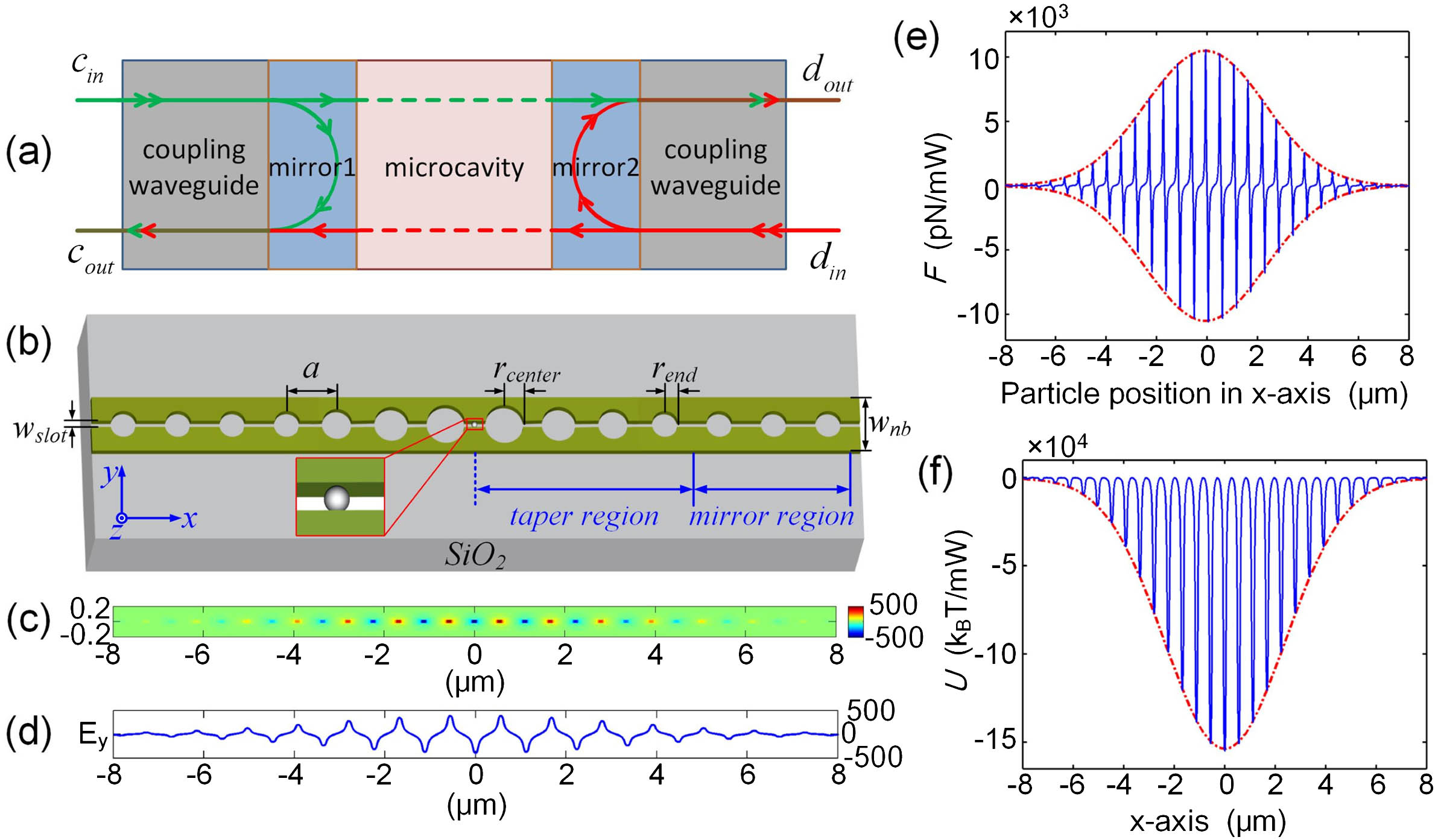
Figure 1.(a) Schematic of the theoretical analysis model, which is a symmetric mirror/microcavity/mirror system. (b) Schematic of a nanoslotted-1D-PC nanobeam cavity for optical trapping. The structure is symmetric with respect to its center (blue dashed line). The trapped nanoparticle is shown within the slot. (c) Calculated distribution (top view with ) of the fundamental resonant mode in the microcavity. (d) profile along the centerline of the cavity in the -direction. The units of the -axis are micrometers (μm). (e) Optical trapping force distribution profile and (f) trapping potential distribution profile along the centerline of the cavity in the -direction (solid line) and fitted Gaussian envelope function (dashed line), respectively, where , , , , , , , and are chosen.
The intracavity energy , reflectivity , and transmissivity can be derived from Eq. (2) [54] as follows:
It is found that when the detuning is much larger than the linewidth, i.e., , the light frequency falls into the PBG and the cavity mode cannot be excited efficiently, resulting in and almost being zero. When the cavity mode is on resonance, i.e., , and achieve maximum values as follows:
Here, we take a PS nanoparticle with radius as the trapped object. The optical trapping force () to a PS nanoparticle in the microcavity includes the gradient force and the scattering force. Furthermore, the scattering force is neglected due to the equilibrium of the standing wave mode. Thus, the gradient force can be calculated by regarding the particle as a dipole [3]:where represents the dipole moment of the particle. represents the polarizability of the sphere. By rewriting Eq. (5), the gradient force can be expressed as a function of intracavity energy and the relative field intensity distribution of that point, given as where represents the mode volume of the cavity and represents the relative intensity distribution. Considering the variation of the field intensity within the particle, can be replaced by the average relative field intensity where represents the volume of PS nanoparticles. As seen in Eq. (6), the optical trapping force is proportional to (i.e., ) for a nanoparticle at the fix point. Furthermore, the trapping potential can be easily derived from Eq. (6), expressed as
3. NANOSLOTTED-1D-PC NANOBEAM CAVITY DESIGN
In this work, to validate the theoretical analysis in the above section, the basic structure of our design is a silicon-channel-waveguide-based nanoslotted-1D-PCNC. The schematic of the proposed nanoslotted-1D-PCNC is shown in Fig. 1(b). As seen, it is formed by introducing a nanoslotted structure in the middle of a 1D-PCNC, which consists of a single row of hole gratings embedded in a silicon nanobeam waveguide along horizontal -axis, based on a silicon-on-insulator (SOI) platform with a 220 nm thick silicon device layer and a 2 μm thick buffer layer. The refractive indices of the silicon core layer and silica insulator layer are taken as and , respectively. The top cladding is assumed to be air () in our numerical simulation [10,50]. To make the proposed device operate at the telecom wavelength range (), the thickness and width of the silicon nanobeam waveguide are kept fixed as and , respectively. The periodicity of the hole gratings is to form a PC lattice. The structure is symmetric with respect to the center [the blue dashed line in Fig. 1(b)]. A basic 1D-PCNC cavity is formed by decreasing radii of the hole gratings while keeping the periodicity (), slot width (), and nanobeam waveguide width unchanged. To achieve a high quality factor () [55], (i) the hole gratings’ radii in the taper region of the proposed cavity are parabolically tapered from in the center to on both sides, i.e., , where increases from 1 to and represents the hole gratings’ number in the taper region of the cavity. Here, the radii of the hole gratings and are chosen from the numerical band diagram simulations [56]. (ii) The hole gratings’ radii in the mirror region of the proposed cavity are kept fixed as , where increases from 1 to and represents the hole gratings’ number in the mirror region of the cavity. The design of the parabolically tapered hole structure is based on mode matching, which produces a significantly enhanced -factor and optical transmission through reductions in propagation losses and scattering that occur locally at transitions between the taper region and the mirror region of the cavity.
Without loss of generality, TE-like cavity modes with electric field () mainly parallel to the plane of the waveguide are considered in this work. Figures 1(c) and 1(d) show the top view of the major field () distribution profile of the fundamental resonant mode in the proposed cavity. It can be seen clearly that the maximum of the electric field occurs in the nanoslotted area at the center of the cavity, and the field distribution of fundamental resonant mode is highly concentrated. As shown in Fig. 1(e), the corresponding optical trapping forces () induced by the more concentrated mode will be stronger because of resonant enhancement and its sharp intensity gradient. Figure 1(f) shows the optical trapping potential () distribution profile along the centerline of the cavity in the -direction. As seen, at the center of the cavity, the largest potential depth occurs. Thus, the nanoparticle will be stably trapped in this area due to the huge trapping potential depth of the cavity.
Next, to investigate the interaction between the nanoparticle and the target resonant mode field distribution confined within the cavity, the proposed nanoslotted-1D-PCNCs with different slot widths (), number () of hole gratings in the taper region, and number () of hole gratings in the mirror region are discussed in detail. Here, the trapped object is taken as a PS nanoparticle with radius and refractive index (for the wavelength near infrared). In the simulation, the trapped PS nanoparticle is placed at the vertical center with 50 nm separation between the cavity center corner (also the stable trapping position at , , and ). That is, the trapped nanoparticle is centered at , , and . The optical trapping force is calculated by integrating the Maxwell stress tensor on the outer surface of the PS nanoparticle [28]. In this section, we consider the case when a waveguide mode is inserted into the cavity structure for one end of the coupling waveguide.
First, we investigate the effect of different slot widths () on the cavity transmissivity (), , trapping potential (), and the induced optical trapping force (, along the -direction) on the PS nanoparticle, when changes from to , while other parameters are kept fixed as , , , , , , and . The optical trapping force is normalized by input power in units of pN/mW. Figure 2(a) shows the cavity transmissivity () and as functions of different slot widths. As seen, with the slot width increased, the cavity transmissivity increases. In addition, when the slot width is between and , ultrahigh over is achieved. Figure 2(b) shows the maximum optical trapping force () and trapping potential () on the 10 nm radius PS nanoparticle along the -direction as a function of slot width. As seen, when the slot width is , an optical trapping force as high as and a trapping potential as high as can be achieved. Here we set to be room temperature as 300 K (). Figure 2(c) shows the electric field distribution (top view) of the fundamental mode taken at the center of the silicon layer () as a function of slot width changed as , 20, 40, 60, 80, 100, 150, and 200 nm, respectively. As seen, compared to the nonslotted cavity structure (), the proposed nanoslotted cavity structure can effectively confine light within the cavity, allowing combined hollow-core and liquid-core behavior and creating strong optical intensities and gradients. Here, we choose the slot width as in the following simulation.

Figure 2.Influence of different slot widths on (a) cavity transmissivity and , (b) maximum optical trapping force and trapping potential on a 10 nm radius PS nanoparticle, and (c) electric field distributions (top view) taken at the center of the silicon layer () when is changed from 0 to 200 nm and other parameters are kept fixed as , , , , , , and .
Second, from Eq. (6), we know that the optical trapping force is proportional to . That means that other than designing a suitable resonant mode with high , the efficient coupling between the input/output waveguide mode and the cavity resonant mode with high transmissivity () for efficient nanoparticle trapping needs to be considered. Thus, we change the period hole gratings’ number (changed from to ) in the taper region and (changed from to ) in the mirror region of the cavity [Fig. 1(b)], respectively, and investigate the effect of different values of and on the cavity transmissivity , , trapping potential , and the induced optical trapping force (along the -direction) on the 10 nm radius PS nanoparticle, when other parameters are kept fixed as , , , , , and , as shown in Fig. 3. As seen in Fig. 3(e), when and , the maximum optical trapping force on the 10 nm radius PS nanoparticle as high as can be achieved. A trapping potential as high as can be achieved, which is enhanced by more than two orders of magnitude compared to the previous work [40,49,53]. When is larger than 5 (), enough for the nanoslotted photonic crystal lattice to provide the PBG effect, the proposed device can confine the resonant mode very well with ultrahigh over [shown as versus in Fig. 3(d)]. However, the good PBG effect reduces the coupling efficiency between the input/output waveguide mode and the cavity resonant mode [shown as versus in Fig. 3(d)], resulting in low cavity transmission. Thus, the optical trapping force induced by the weakly coupled resonance is rather small. On the contrary, when is reduced and less than 5 (), the cavity decreases because the confinement provided by the cavity PBG effect becomes weaker. For even smaller , because the cavity resonant mode can no longer be supported by the insufficient PBG effect, resulting in the cavity decreased sharply and no resonance enhancing the optical trapping force, the induced optical trapping force becomes weaker again. As known from Section 2, the optical trapping force is proportional to the energy of the cavity. Thus, the maximum optical trapping force can be obtained in the case of a cavity with the largest energy. From Eq. (4), the energy stored in the cavity achieves its maximum when for a given , namely, . As seen in Fig. 3(d), the simulation results show that when and , the optical trapping force achieves the maximum value at the transmission of the cavity , namely, the cavity transmission (near 0.25), which is in accordance with the theoretical analysis and the previous work [40,49]. Figures 3(c) and 3(f) display that the optical trapping force () varies with . As seen, the normalized optical trapping force () is proportional to , which further verifies the theoretical analysis in Section 2.
Figure 3.Influence of different hole grating numbers (changed from to ) in the taper region of the cavity on (a) cavity transmissivity and , and (b) maximum optical trapping force and trapping potential on a 10 nm radius PS nanoparticle when . Influence of different hole grating numbers (changed from to ) in the mirror region of the cavity on (d) cavity transmissivity and , and (e) maximum optical trapping force and trapping potential on a 10 nm radius PS nanoparticle when . For both cases, other parameters are kept fixed as , , , , , and . (c), (f) Normalized optical trapping force for the proposed cavity with different values of .
4. NUMERICAL RESULTS AND DISCUSSION
Herein, based on the simulation results and optimization process discussed in Section 3, a summary to show the structure parameters for the optimized nanoslotted-1D-PCNC are as follows: , , , , , , , and . To characterize the maximum optical trapping force in this system, the detailed numerical analysis and simulations performed here are based on the three-dimensional finite element method (3D-FEM). To determine the optical trapping force exerted on a PS nanoparticle, a virtual spherical surface enclosing the nanoparticle surface is constructed, and the electromagnetic field on this surface is calculated. Here, the size of the virtual surface is the same as the surface of the enclosed nanoparticle. Then, by evaluating the time-independent Maxwell stress tensor and integrating it over the closed surface that encloses the PS nanoparticle, the optical trapping force can be obtained. Here, the numerical technique consists of repeatedly calculating the optical trapping force while shifting the PS nanoparticle’s physical position along one of the main axes [Fig. 1(b)]. When canning the nanoparticle along the - and -axes, the virtual surface moves with the nanoparticle. Figures 4(a) and 4(b) display the plots of the normalized optical trapping force profile for a 10 nm radius PS nanoparticle that is displaced in - and -dimensions from the stable trapping position (namely, the cavity center with , , and ). As seen, the theoretical calculation results (solid blue line with plus sign) are consistent with the 3D-FEM numerical simulation results (dashed red line added with square). Figure 4(a) shows the trapping force (, component) for a 10 nm radius PS nanoparticle as it is located within the slot center ( and ) and displaced along the length of the nanoslotted-1D-PCNC (-axis). The zero -axis value corresponds to the stable trapping position at the cavity center. As can be seen, because the nanoslotted-1D-PCNC structure is symmetric horizontally in the -direction, the horizontal component optical force exerted on the nanoparticle in the -direction is mirror symmetric with respect to the cavity center. The trapping force is negative for , which means that when some perturbation floats the nanoparticle slightly away from the cavity center, the strength of the trapping force increases progressively to pull the nanoparticle back toward the cavity center. As seen in Fig. 4(a), the trapping force () reaches a maximum at the point () where the field gradient is strongest at the entrance between the nanoslot waveguide and the hole grating. By using 3D-FEM, the simulated maximum optical trapping force for a 10 nm radius PS nanoparticle of is observed, which is two orders of magnitude higher than the maximum trapping force in the case of recent photonic crystal nanobeam cavities [40–42,47,49] and several orders of magnitude higher than other optical trapping techniques based on nanoslotted waveguides [27,28]. In addition, when the nanoparticle floats away further in the -direction (), the strength of the trapping force declines along the -direction as the nanoparticle position in the -axis increases. That represents the characteristic of the evanescent field and indicates that the guided wave will lose its effect upon the nanoparticle. Figure 4(b) illustrates the vertical trapping forces (, component) exerted on a 10 nm radius PS nanoparticle for varying vertical positions along the height of the nanoslotted-1D-PCNC (-axis) as it is located within the slot center ( and ). Qualitatively, we note that (i) the vertical trapping force is negative for , which means nanoparticles that are located above the cavity center tend to exhibit a net downward force. This indicates that the optical gradient in the cavity tends to guide nanoparticles toward the middle of the device structure where the intensity is at its maximum. (ii) The vertical trapping force attains its maximum value at corresponding to half of the thickness of the silicon device layer. (iii) Once the vertical trapping force reaches its maximum value, it declines to zero as the nanoparticle position in -axis increases, which represents the decay of the evanescent-wave-behaving region of the cavity structure.
Figure 4.Numerical analysis of optical trapping forces for the proposed nanoslotted-1D-PCNC device. All theoretically computed and 3D-FEM simulated trapping forces listed are normalized by input power in units of pN/mW. Trapping force profiles of (a) and (b) for the PS nanoparticle as it is moved along the -axis and -axis of the device, respectively. In both (a) and (b), all calculations are done for a PS nanoparticle with a radius of 10 nm. Trapping potential distributions experienced by the PS nanoparticle along (c) the -direction (ranging from to ) and (d) the -direction (ranging from to ).
By integrating the trapping force along the -axis (ranging from to ) with and along the -axis (ranging from to ) with , respectively, the corresponding potential experienced by the PS nanoparticle can be obtained. Figures 4(c) and 4(d) show the corresponding potential distribution in the - and -direction, respectively. A criterion widely used for stable trapping requires depth of the potential energy () larger than [3,40]. As seen in Figs. 4(c) and 4(d), based on 3D-FEM simulation results (red line), depths of the trapping potential () along - and -directions as large as and are obtained, respectively, which are much deeper than the stable trapping requirement. Thus, the results manifest the trapping ability of the proposed slotted-1D-PCNC.
From the calculated optical trapping force and trapping potential in Fig. 4, two parameters can commonly be extracted to describe optical trapping: one is the trapping stiffness (), and the other is the trapping stability (). In this system, for distances not far from the stable position, namely, the equilibrium point, the response of the optical trapping force is similar to a linear spring where the spring constant is equal to the trapping stiffness. Therefore, the trapping stiffness in the -direction () and the -direction () is the derivative of the restoring force and , respectively, with respect to the position perturbation around the equilibrium point, and can be described as follows [41]:
Here, the other parameter of interest is the trapping stability (), which leads to the average trapping time proportional to its exponential following a Kramers escaper process [57]. So the trapping stability () can be defined as the ratio of the potential energy depth () to the available thermal energy [41]:
Based on the optical trapping characteristics of the proposed nanoslotted-1D-PCNC design shown in Fig. 4, for a PS nanoparticle with a 10 nm radius, the calculated trapping stiffnesses in the -direction and the -direction are found to be and , respectively. The estimated trapping stiffness for this system is more than three orders of magnitude higher than those of the conventional photonic crystal nanobeam resonators [41,42] and more than two orders of magnitude higher than that of the recent slotted photonic crystal cavity [53]. In addition, as alluded to above, the trapping stability is the ratio of the work energy required to remove the nanoparticle from the trap to the random thermal energy in the system. Based on Eq. (11), trapping stabilities as large as are achieved in the proposed nanoslotted-1D-PCNC design. In order to achieve a stability factor equal to 10, which is generally considered sufficient to achieve stable trapping despite the presence of Brownian motion [3,53], the threshold power for stable trapping in this system is only 0.087 μW. A significant decrease of the optical power required for stable trapping can be achieved compared to previous designs, e.g., the power requirement for the stable trapping of a 25 nm radius PS nanoparticle in the slotted 2D-PC cavity (27 μW) [53], and the power requirement for the stable trapping of a 50 nm radius PS nanoparticle in the recent 1D-PC cavity with waist design (320 μW) [40]. Thus, the proposed optical trapping scheme based on nanoslotted-1D-PCNC in this work is a promising platform for achieving efficient trapping. In addition, we have summarized the trapping performances of different optical trapping schemes, as shown in Table 1. Here, although the performances of these different optical trapping systems shown in the table are not strict comparisons because they were performed with different size PS particles, we can find that the trapping performance of the proposed slotted-1D-PCNC is greatly improved compared with those of other optical trapping systems. The superposition of evanescent fields leads to an increase in the field intensity, as shown in Fig. 1(c). Thus, the optical force on a nanoparticle is enhanced by orders of magnitude, and the trapping stiffness is also significantly increased.
| Trapping System | Trapping Particle Radius (nm) | Trapping Force (pN/mW) | Trapping Potentiala(kBT/mW) | Trapping Stiffness (pN·nm−1 ·mW−1) | Threshold Power (μW) | References |
| Solid waveguide | PS, 250 | 0.025 | — | — | — | [25] |
| Slotted waveguide | PS, 10 | 0.007 | 1.4 | 1.31×10⁻⁴ | 7.14×10³ | [28] |
| Ring resonator | PS, 250 | 0.16 | 5.56 | 3.7×10⁻⁴ | 1.8×10³ | [29] |
| 2D-PC | PS, 250 | 3.85 | 76.9 | 0.3 | 130 | [39] |
| 1D-PC | PS, 50 | 2.3 | 31.3 | — | 320 | [40] |
| PS, 50 | 4.2 | 51 | 2.23×10⁻² | 196 | [41] |
| PS, 100 | 330 | — | — | — | [49] |
| Slotted 2D-PC | PS, 25 | 46 | 3.77×10² | 0.34 | 27 | [53] |
| Slotted 1D-PCNC | PS, 10 | 8.28×10³ | 1.15×10⁵ | 167 | 8.70×10⁻² | Present work |
Table 1. Trapping Force, Trapping Potential, Trapping Stiffness, and Threshold Power of Various Optical Trapping Schemes
So far, during the numerical results and discussion above, we have shown that a PS nanoparticle as small as 10 nm in radius can be stably trapped by the 1D-PCNC with the nanoslotted structure. In addition, it has already been outlined that for this type of 1D-PCNC device, the position and size of the nanoparticle within the slot/hole can affect the cavity resonant wavelength. By using 3D-FEM simulation, Fig. 5(a) displays the relation between the trapped single PS nanoparticle with different radii and the corresponding resonant peak wavelength of the transmission spectrum. Each of these trapped PS nanoparticles is positioned at the cavity center at , , and . As seen, trapping of a single 25 nm radius PS nanoparticle causes a 0.6 nm redshift in peak wavelength, which is consistent with the results presented in previous designs [40,41,53]. Although the wavelength shift is small, it is still can be detected due to the narrow linewidth. Thus, the proposed nanoslotted-1D-PCNC device can be utilized to detect a single nanoparticle (e.g., dielectric and metallic nanoparticles) by observing the resonant peak wavelength shift in the transmission spectrum as demonstrated in Ref. [50]. Moreover, it also makes it possible to recognize the size of the trapped nanoparticle by the amount of peak shift. Figure 5(b) shows the magnitude of the maximum trapping force in the -direction as a function of the PS nanoparticle with different sizes/radii. Here, the nanoparticle position is maintained at separated from the cavity center in the -axis with , and , as displayed in the inset in Fig. 5(a). As expected, PS nanoparticles of increasing radii experience stronger trapping forces in the nanoslotted-1D-PCNC.
Figure 5.(a) 3D-FEM simulated the resonant peak wavelength of the transmission spectrum of the designed slotted 1D-PCNC when no nanoparticle is trapped and when a PS nanoparticle with a radius of 5, 10, 15, 20, or 25 nm is trapped at the cavity center with , , and . (b) The graph shows the magnitude of the maximum trapping force in the -direction as a function of the PS nanoparticle with different sizes.
5. SUMMARY
In summary, we have designed an ultracompact nanoslotted-1D-PCNC structure for nanoparticle manipulation and detection. In this structure, the advantages of both the 1D-PCNC (ultrahigh ) and the nanoslotted waveguide (strong optical intensities and gradients) are combined to improve optical trapping capabilities so that much smaller nanoparticles can be manipulated. Numerical simulations indicate that the proposed nanoslotted-1D-PCNC can efficiently transport a PS nanoparticle with a diameter as small as 10 nm in a 60 nm slot. Here, excellent optical confinement and strong optical intensities and gradients provided by the device greatly enhance the optical trapping force exerted on the nanoparticle. For trapping a PS nanoparticle of 10 nm radius within the slot of the proposed device, a maximum optical trapping force as high as is obtained. In addition, the investigation of trapping potential shows that a threshold power lower than 0.1 μW is required for stable trapping, more than two orders of magnitude reduced compared to recent photonic-crystal-based optical trapping systems. Moreover, the numerical simulations show that the trapping of a single 25 nm radius PS nanoparticle causes a 0.6 nm redshift in resonant peak wavelength, which is consistent with the results presented in previous designs. Thus, the proposed device can be used for single nanoparticle detection by observing the resonant wavelength shift. Moreover, it also makes it possible to recognize nanoparticle size by analyzing the amount of wavelength shift. Therefore, the device presented in this work can potentially become a versatile platform for single nanoparticle, molecule, or virus manipulation and detection and other lab-on-a-chip applications in the future.
Acknowledgment
Acknowledgment. The authors thank Xiao-Chong Yu for fruitful discussions and help with simulations.
References
[1] D. Erickson, X. Serey, Y. Chen, S. Mandal. Critical review: nanomanipulation using near field photonics. Lab Chip, 11, 995-1009(2011).
[2] D. G. Grier. A revolution in optical manipulation. Nature, 424, 810-816(2003).
[3] A. Ashkin, J. M. Dziedzic, J. E. Bjorkholm, S. Chu. Observation of a single-beam gradient force optical trap for dielectric particles. Opt. Lett., 11, 288-290(1986).
[4] A. N. Grigorenko, N. W. Roberts, M. R. Dickinson, Y. Zhang. Nanometric optical tweezers based on nanostructured substrates. Nat. Photonics, 2, 365-370(2008).
[5] A. Ashkin. History of optical trapping and manipulation of small-neutral particle, atoms, and molecules. IEEE J. Sel. Top. Quantum Electron., 6, 841-856(2000).
[6] A. Ashkin. Acceleration and trapping of particles by radiation pressure. Phys. Rev. Lett., 24, 156-159(1970).
[7] K. C. Neuman, S. M. Block. Optical trapping. Rev. Sci. Instrum., 75, 2787-2809(2004).
[8] A. Ashkin, J. M. Dziedzic, T. Yamane. Optical trapping and manipulation of single cells using infrared laser beams. Nature, 330, 769-771(1987).
[9] P. W. H. Pinkse, T. Fischer, P. Maunz, G. Rempe. Trapping an atom with single photons. Nature, 404, 365-368(2000).
[10] L. Jauffred, S. M. R. Taheri, R. Schmitt, H. Linke, L. B. Oddershede. Optical trapping of gold nanoparticles in air. Nano Lett., 15, 4713-4719(2015).
[11] E. Vetsch, S. T. Dawkins, R. Mitsch, D. Reitz, P. Schneeweiss, A. Rauschenbeutel. Nanofiber-based optical trapping of cold neutral atoms. IEEE J. Sel. Top. Quantum Electron., 18, 1763-1770(2012).
[12] M. J. Morrissey, K. Deasy, M. Frawley, R. Kumar, E. Prel, L. Russell, V. G. Truong, S. N. Chormaic. Spectroscopy, manipulation and trapping of neutral atoms, molecules, and other particles using optical nanofibers: a review. Sensors, 13, 10449-10481(2013).
[13] J. Huang, X. Liu, Y. Zhang, B. Li. Optical trapping and orientation of Escherichia coli cells using two tapered fiber probes. Photon. Res., 3, 308-312(2015).
[14] F. Lindenfelser, B. Keitch, D. Kienzler, D. Bykov, P. Uebel, M. A. Schmidt, P. St. J. Russell, J. P. Home. An ion trap built with photonic crystal fibre technology. Rev. Sci. Instrum., 86, 033107(2015).
[15] D. Grass, J. Fesel, S. G. Hofer, N. Kiesel, M. Aspelmeyer. Optical trapping and control of nanoparticles inside evacuated hollow core photonic crystal fibers. Appl. Phys. Lett., 108, 221103(2016).
[16] M. D. Baaske, F. Vollmer. Optical observation of single atomic ions interacting with plasmonic nanorods in aqueous solution. Nat. Photonics, 10, 733-739(2016).
[17] Y. Zhi, X. Yu, Q. Gong, L. Yang, Y. Xiao. Single nanoparticle detection using optical microcavities. Adv. Mater., 29, 1604920(2017).
[18] B. Li, W. R. Clements, X. Yu, K. Shi, Q. Gong, Y. Xiao. Single nanoparticle detection using split-mode microcavity Raman lasers. Proc. Natl. Acad. Sci. USA, 111, 14657-14662(2014).
[19] L. Shao, X. Jiang, X. Yu, B. Li, W. R. Clements, F. Vollmer, W. Wang, Y. Xiao, Q. Gong. Detection of single nanoparticles and lentiviruses using microcavity resonance broadening. Adv. Mater., 25, 5616-5620(2013).
[20] J. Zhu, Y. Zhong, H. Liu. Impact of nanoparticle-induced scattering of an azimuthally propagating mode on the resonance of whispering gallery microcavities. Photon. Res., 5, 396-405(2017).
[21] M. L. Juan, M. Righini, R. Quidant. Plasmon nano-optical tweezers. Nat. Photonics, 5, 349-356(2011).
[22] K. Wang, E. Schonbrun, P. Steinvurzel, K. B. Crozier. Trapping and rotating nanoparticles using a plasmonic nano-tweezer with an integrated heat sink. Nat. Commun., 2, 469-475(2011).
[23] J. C. Ndukaife, A. V. Kildishev, A. Nnanna, V. M. Shalaev, S. T. Wreley, A. Boltasseva. Long-range and rapid transport of individual nano-objects by a hybrid electrothermoplasmonic nanotweezer. Nat. Nanotechnol., 11, 53-59(2016).
[24] Z. Chen, F. Zhang, Q. Zhang, J. Ren, H. Hao, X. Duan, P. Zhang, T. Zhang, Y. Gu, Q. Gong. Blue-detuned optical atom trapping in a compact plasmonic structure. Photon. Res., 5, 436-440(2017).
[25] B. S. Schmidt, A. H. J. Yang, D. Erickson, M. Lipson. Optofluidic trapping and transport on solid core waveguides within a microfluidic device. Opt. Express, 15, 14322-14334(2007).
[26] T. H. Stievater, D. A. Kozak, M. W. Pruessner, R. Mahon, D. Park, W. S. Rabinovich, F. K. Fatemi. Modal characterization of nanophotonic waveguides for atom trapping. Opt. Mater. Express, 6, 3826-3837(2016).
[27] A. H. J. Yang, S. D. Moore, B. S. Schmidt, M. Klug, M. Lipson, D. Erickson. Optical manipulation of nanoparticles and biomolecules in sub-wavelength slot waveguides. Nature, 457, 71-75(2009).
[28] A. H. J. Yang, T. Lerdsuchatawanich, D. Erickson. Forces and transport velocities for a particle in a slot waveguide. Nano Lett., 9, 1182-1188(2009).
[29] S. Y. Lin, E. Schonbrun, K. Crozier. Optical manipulation with planar silicon microring resonators. Nano Lett., 10, 2408-2411(2010).
[30] P. T. Lin, P. T. Lee. All-optical controllable trapping and transport of subwavelength particles on a tapered photonic crystal waveguide. Opt. Lett., 36, 424-426(2011).
[31] M. G. Scullion, Y. Arita, T. F. Krauss, K. Dholakia. Enhancement of optical forces using slow light in a photonic crystal waveguide. Optica, 2, 816-821(2015).
[32] N. D. Gupta, V. Janyani. Design and analysis of light trapping in thin film GaAs solar cells using 2-D photonic crystal structures at front surface. IEEE J. Sel. Top. Quantum Electron., 53, 4800109(2017).
[33] M. Barth, O. Benson. Manipulation of dielectric particles using photonic crystal cavities. Appl. Phys. Lett., 89, 253114(2006).
[34] A. Rahmani, P. C. Chaumet. Optical trapping near a photonic crystal. Opt. Express, 14, 6353-6358(2006).
[35] T. Tanabe, M. Notomi, E. Kuramochi, A. Shinya, H. Taniyama. Trapping and delaying photons for one nanosecond in an ultrasmall high-Q photonic-crystal nanocavity. Nat. Photonics, 1, 49-52(2007).
[36] C. A. Mejia, N. Huang, M. L. Povinelli. Optical trapping of metal-dielectric nanoparticle clusters near photonic crystal microcavities. Opt. Lett., 37, 3690-3692(2012).
[37] N. Descharmes, U. P. Dharanipathy, Z. Diao, M. Tonin, R. Houdre. Observation of backaction and self-induced trapping in a planar hollow photonic crystal cavity. Phys. Rev. Lett., 110, 123601(2013).
[38] A. Nirmal, A. K. K. Kyaw, J. Wang, K. Dev, X. Sun, H. V. Demir. Light trapping in inverted organic photovoltaics with nanoimprinted ZnO photonic crystals. IEEE J. Photovoltaics, 7, 545-549(2017).
[39] M. Tonin, F. M. Mor, L. Forro, S. Jeney, R. Houdre. Thermal fluctuation analysis of singly optically trapped spheres in hollow photonic crystal cavities. Appl. Phys. Lett., 109, 241107(2016).
[40] P. T. Lin, T. W. Lu, P. T. Lee. Photonic crystal waveguide cavity with waist design for efficient trapping and detection of nanoparticles. Opt. Express, 22, 6791-6800(2014).
[41] X. Serey, S. Mandal, D. Erickson. Comparison of silicon photonic crystal resonator designs for optical trapping of nanomaterials. Nanotechnology, 21, 305202(2010).
[42] S. Mandal, X. Serey, D. Erickson. Nanomanipulation using silicon photonic crystal resonators. Nano Lett., 10, 99-104(2010).
[43] D. Yang, B. Wang, X. Chen, C. Wang, Y. Ji. Ultracompact on-chip multiplexed sensor array based on dense integration of flexible 1-D photonic crystal nanobeam cavity with large free spectral range and high Q-factor. IEEE Photon. J., 9, 4900412(2017).
[44] Y. Chen, X. Serey, R. Sarkar, P. Chen, D. Erickson. Controlled photonic manipulation of proteins and other nanomaterials. Nano Lett., 12, 1633-1637(2012).
[45] S. Lin, W. Zhu, Y. Jin, K. B. Crozier. Surface-enhanced Raman scattering with Ag nanoparticles optically trapped by a photonic crystal cavity. Nano Lett., 13, 559-563(2013).
[46] C. Renaut, B. Cluzel, J. Dellinger, L. Lalouat, E. Picard, D. Peyrade, E. Hadji, F. Fornel. On chip shapeable optical tweezers. Sci. Rep., 3, 2290(2013).
[47] C. Ciminelli, D. Conteduca, F. DellOlio, M. N. Armenise. Design of an optical trapping device based on an ultra-high Q/V resonant structure. IEEE Photon. J., 6, 0600916(2014).
[48] H. Du, X. Zhang, J. Deng, Y. Zhao, F. S. Chau, G. Y. Zhou. Lateral shearing optical gradient force in coupled nanobeam photonic crystal cavities. Appl. Phys. Lett., 108, 171102(2016).
[49] S. Han, Y. Shi. Systematic analysis of optical gradient force in photonic crystal nanobeam cavities. Opt. Express, 24, 452-458(2016).
[50] F. Liang, Q. Quan. Detecting single gold nanoparticles (1.8 nm) with ultrahigh-q air mode photonic crystal nanobeam cavities. ACS Photon., 2, 1692-1697(2015).
[51] J. T. Robinson, C. Manolatou, L. Chen, M. Lipson. Ultrasmall mode volumes in dielectric optical microcavities. Phys. Rev. Lett., 95, 143901(2005).
[52] COMSOL Inc.
[53] J. Ma, L. J. Martinez, M. L. Povinelli. Optical trapping via guided resonance modes in a Slot-Suzuki-phase photonic crystal lattice. Opt. Express, 20, 6816-6824(2012).
[54] J. D. Joannopoulos, S. G. Johnson, J. N. Winn, R. D. Meade. Photonic Crystals: Molding the Flow of Light(2008).
[55] D. Yang, S. Kita, F. Liang, C. Wang, H. Tian, Y. Ji, M. Lonar, Q. Quan. High sensitivity and high Q-factor nanoslotted parallel quadrabeam photonic crystal cavity for real-time and label-free sensing. Appl. Phys. Lett., 105, 063118(2014).
[56] D. Yang, H. Tian, Y. Ji. High-Q and high-sensitivity width-modulated photonic crystal single nanobeam air-mode cavity for refractive index sensing. Appl. Opt., 54, 1-5(2015).
[57] C. W. Gardiner. Handbook of Stochastic Methods: For Physics, Chemistry, and the Natural Sciences(2004).


