Abstract
Natural surface-enhanced Raman spectroscopy (SERS) chips based on plants or insects have gained increased attention due to their facile characteristics and low costs. However, such chips remain a major challenge for practical application because of poor reproducibility and stability as well as unavoidable damage to the surface structure during coating metal and uncontrolled dehydration. By using a simple wrinkling method, we develop a new route to fabricate a low-cost bionic SERS chip for practical detection. Inspired by the taro leaf, we fabricate a SERS chip with a super-hydrophobic and plasmonic micro/nano dual structure, and its structure parameters can be optimized. Compared with the natural taro-leaf SERS chip, our artificial chip exhibits Raman signals with an order of magnitude higher sensitivity () and enhancement factor () under the illumination of weak laser radiation, demonstrating that our SERS chip has great potential in biological detection. The excellent performances of our bionic SERS chip are attributed to a synergy of optimized micro-wrinkle and nano-nest, which is verified by experiment and simulation. We believe our bionic chip could be a promising candidate in practical application due to its merits such as simple fabricating process, optimizable structure, low cost, excellent homogeneity, high sensitivity, and stability.1. INTRODUCTION
Surface-enhanced Raman spectroscopy (SERS) is a powerful and widely used tool for the identification and detection of various chemical and biological molecules [1–5]. The SERS chips with noble-metal surfaces and plasmonic nanostructures are especially suitable for ultra-sensitivity, low-concentration detection, and even single-molecule detection (SMD) because of the localized surface plasmon resonance (LSPR) [6–8], which occurs when analytes are adsorbed on the plasmonic nanostructures; thus, the strong localized electric field (hot spots) is generated and greatly enhances their Raman signals. Typical SERS chips are fabricated by complicated processes, such as focused ion beam and e-beam lithography and photolithography [2], which are time-consuming, expensive, and with low-throughput. In addition, some assembly methods based on chemical synthesis [9–11] or galvanic displacement reaction [12] for fabricating SERS chips are relatively simple, but their structures or configurations are difficult to optimize.
Recently, the biological materials with micro/nano structures from the natural world have been used as one type of emerging SERS chip because of simple processes and low costs [1,13–16]. Here are some examples: Xu et al. developed SERS substrates based on an Ag-coated rose petal achieving a detection limit low to [13]; Mu et al. developed SERS substrates based on butterfly wings achieving a detection limit of [15]; Huang et al. developed an SERS chip based on an Ag-coated taro-leaf achieving a detection limit of [16]. These biological surfaces have an innate hierarchical structure composed of micro/nano structures, which do not only provide rich plasmonic hot spots but also exhibit super-hydrophobicity for analyte enrichment. However, two main shortages in such natural SERS chips hinder their practical applications: one is that the frail biological micro/nano structures will be unavoidably damaged in the process of noble-metal deposition and uncontrolled dehydration; the other is more fatal, i.e., the all-natural structures are inhomogeneous and thus have poor reproducibility of the Raman signal in different regions. These lead to the fact that, at present, such biological SERS chip is still impractical for real-life usage. Obviously, utilizing optimized bionic structures instead of innate biologic structures could improve the reproducibility and homogeneity of the chips to meet the urgent practical need. Thus, developing a simple and low-cost method for fabricating a good-performance artificial SERS chip is necessary.
In this work, inspired by the taro-leaf hierarchical structure [16], we fabricate a large-area bionic or pseudo-bionic SERS chip with a micro/nano dual structure by a simple and low-cost method. Such artificial SERS chip is demonstrated to have unique super-hydrophobicity and rich plasmonic hot spots, exhibiting an order of magnitude higher sensitivity () and enhancement factor () of Raman signals than natural taro-leaf SERS chips. Moreover, our further experimental and theoretical analyses indicate that the micro/nano structures on the chip are jointly responsible for the good SERS performance.
Sign up for Photonics Research TOC. Get the latest issue of Photonics Research delivered right to you!Sign up now
2. EXPERIMENTAL SECTION
A. Fabrication of the Hierarchical Structure SERS Chip
First, the polyvinyl chloride (PVC) shrink sheets were coated with different thickness of Ag thin films by magnetron sputtering. The sputtering power was 100 W, and the Ar gas flux was 25 sccm, in which case the sputtering rate was about ; thus, the Ag thickness (10–50 nm) was controlled by the sputtering time (60–300 s). Second, the micro-wrinkle structure was formed after the Ag-coated PVC films are heated at 140°C in about 10 min for a thermal shrink process. Third, the amorphous thin film was deposited on the wrinkled PVC/Ag bilayer by sputtering Bi with Ar (20 sccm) and (5 sccm), and then the sample was immersed in 0.05 M HCl solution to generate the BiOCl nano-nest structure. Finally, a layer of Ag thin film about 20 nm was coated again on the micro/nano dual structure. Magnetron sputtering was performed by a magnetron sputtering system (Kurt J. Lesker, PVD7), and the Ag and Bi targets (purity 99.99%) were purchased from the General Research Institute for Nonferrous Metals, Beijing, China.
B. Chip Characterization and R6G SERS Detection
The morphology and energy dispersive spectrometry (EDS) of the chip were characterized by a scanning electron microscope (SEM, Hitachi-4800). The crystal structure of the chip surface was characterized by X-ray diffraction (XRD, D8 focus, Bruker). Static water contact angle (CA) was measured with an OCA20 contact angle system (Dataphysics Instruments GmbH, Germany). Rhodamine 6G (R6G) solutions with concentration from to were prepared, and then a 4 μL R6G solution was dropped on the chip sample, and the drop was evaporated naturally at room temperature in an ultraclean chamber. Raman spectra were obtained on a micro-Raman spectrometer (Renishaw inVia plus) equipped with a liquid-nitrogen-cooled argon ion laser at 514.5 nm. With this laser wavelength, an Ag nanostructure is more suitable than Au for excitation of stronger surface plasmon polaritons (SPPs). The final power lighted on the sample was only 5 μW, which is acquired through attenuating a 10 mW laser power to 0.05%. A finite difference time domain (FDTD) method was used to calculate the electromagnetic field distributions of Y-shaped nano-nest. In the simulation, the structural parameters were set according to the experimental morphology.
3. RESULTS AND DISSCUSION
The process to fabricate the bionic SERS chip with micro/nano dual structure is depicted in Fig. 1(a). First, an Ag thin film was deposited on a PVC shrink sheet and then through a thermal shrink process [17–19] at 140°C for about 10 min; microscale wrinkled structures were generated on the sample surface. Such microstructure was constructed so as to obtain superior hydrophobicity for analyte enrichment. Second, in order to provide enough plasmatic hot spots, a layer of Bi compound was deposited on the wrinkled structure and then immersed in HCl solution to form nest-like BiOCl nanostructures [20–22]. Finally, by coating a layer of Ag again on the sample, our hierarchical SERS chip with micro/nano dual structure similar to the taro leaf was fabricated. Obviously, our method for fabricating the bionic SERS chip is much easier and more affordable than those conventional fabrication methods, including photolithography and e-beam lithography, which are time-consuming and rely on expensive equipment and high-vacuum conditions.
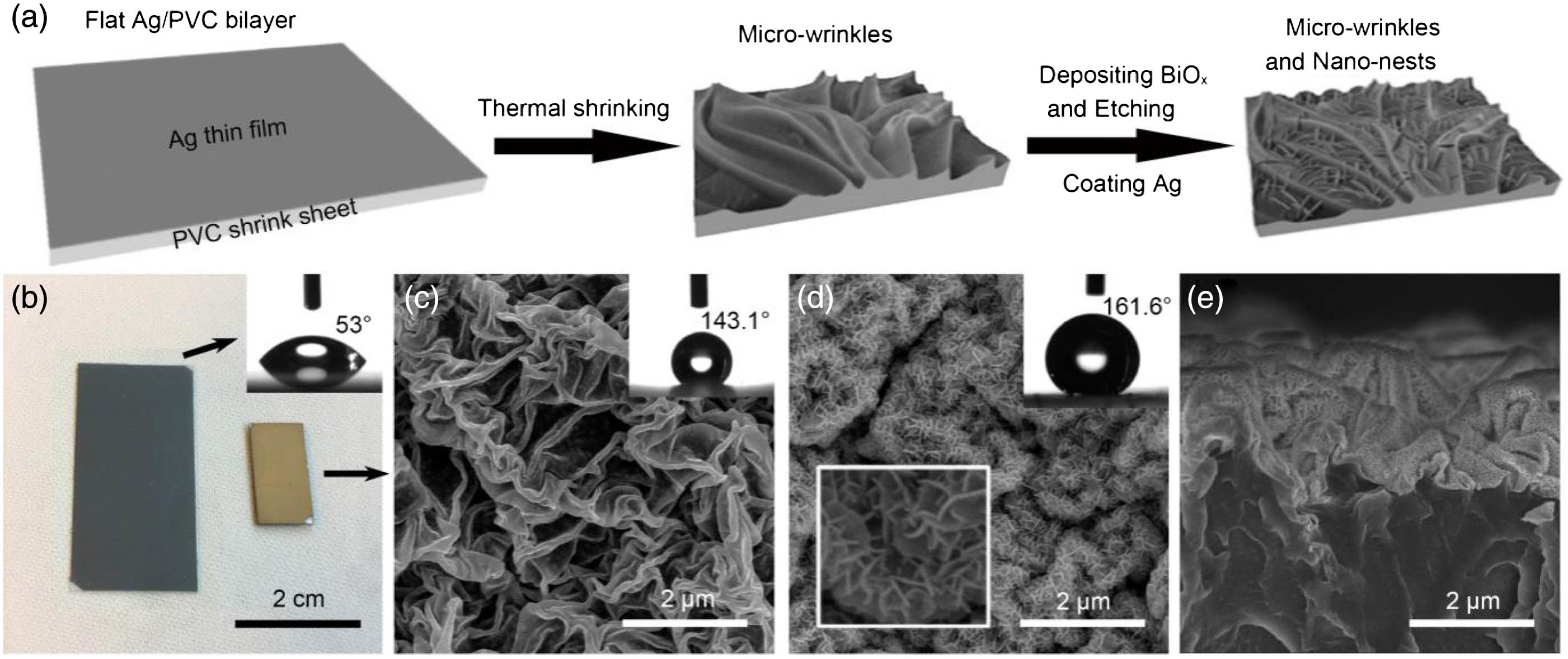
Figure 1.(a) Fabrication procedure of the bionic SERS chip with micro-wrinkles and nano-nests dual structure. (b) Optical photograph of Ag/PVC bilayers before (left) and after (right) thermal shrinking. Inset: CA of the flat sample. (c) SEM image of the micro-wrinkled structure. Inset: CA of the sample with micro-wrinkles. (d) SEM image of the dual structure with micro-wrinkles and nano-nests. Inset (top right): CA of the sample with dual structure. Inset (down left): magnified SEM image of nano-nests. (e) Cross-sectional SEM image of the bionic SERS chip with dual structure.
A typical shrunken Ag/PVC bilayer sample has a water CA of 141.6°, as shown in Fig. 1(c), which is far higher than that of a flat one () without wrinkle structures in Fig. 1(b). The shrink process released plenty of strain; in fact, the shrunken sample was only one-sixth of its original size before heating, as seen in Fig. 1(b). As a result, plentiful wrinkle structures were formed on the surface of a shrunken sheet. Thus, the microstructure should be responsible for the transformation from hydrophilicity () to hydrophobicity (). When Ag-coated nano-nests were added on the wrinkle microstructure, a micro/nano dual structure offering a super-hydrophobic property (CA up to 161.6°) was further demonstrated, as shown in Fig. 1(d). It should be noted that the nanoscale nests were evenly distributed over the microscale wrinkled surface no matter at peaks or valleys. Moreover, any interlayer of the multilayers in the chip shown in Fig. 1(e) is not delaminated, which guarantees better working stability of the chip. In addition, an XRD pattern of the bionic SERS chip in Fig. 2(a) agrees well with the standard spectrum (JCPDS Nos. 04-0783 and 06-0249) [23], and corresponding EDS analysis shown in Fig. 2(b) indicates that there are no other impurities in our chip.

Figure 2.Component analyses via (a) XRD and (b) EDS of the bionic SERS chip.
Generally speaking, the period () of wrinkle microstructure on Ag/PVC bilayer can be determined by the elastic-moduli and thicknesses of the two layers according to the following equation [17]: where and are the moduli of the Ag thin film and the PVC sheet, respectively, and the thickness of the Ag thin film is given by . Here, and are 83 GPa and 2.5 GPa, respectively. On the one hand, Eq. (1) indicates that, for a certain material system and thickness, the period of wrinkle structure is intrinsic, which maintains the good uniformity of our chip. On the other hand, this also provides us with an opportunity to optimize the parameters of the wrinkle structure. The SEM images in Figs. 3(a)–3(e) show the morphology evolution that the period and amplitude of the micro-wrinkles are gradually increased along with the increase of Ag thickness. The wrinkle periods can be controlled by tuning the thickness of the Ag film, and their relationship is plotted in Fig. 3(k). The experimental results are consistent with the theoretical values according to Eq. (1). Therefore, compared with the natural SERS chip with the uncontrollable and irregular microstructure, the micro-wrinkle structure in our bionic chip can be precisely optimized.
Figure 3.(a)–(e) SEM images and corresponding CAs of Ag/PVC micro-wrinkle structures with Ag thickness of 10, 20, 30, 40, and 50 nm, respectively. (f)–(j) SEM images and corresponding CAs of the bionic dual-structure chips with micro-wrinkles and nano-nests. (k) The experimental and theoretical results of wrinkle period for the five Ag/PVC samples with different Ag film thickness in (a)–(e). (l) CA curves of the samples only with micro-wrinkle [black, (a)–(e)] and with dual structure [red, (f)–(j)], respectively. (m) Raman signal intensity of R6G on the different dual-structure chips in (f)–(j).
Optimizing the structure is to optimize the chip properties. Considering that the transformation from a hydrophilic surface () to a hydrophobic one () was induced by the microscale wrinkle structure, we first investigate the dependence of the surface wettability on the surface structures. The period and amplitude of the wrinkle structure have significant influence on hydrophobicity [24]. As shown in the insets of Figs. 3(a)–3(e) and 3(l), the hydrophobicity is intensified with Ag thickness increased from 10 nm to 20 nm (sputtering time from 60 s to 120 s), but no evident change is observed when the thickness is more than 20 nm (sputtering time above 120 s). After adding nano-nests on these samples with micro-wrinkles and coating a layer of Ag again, corresponding contact angles have an increase of about 10° to 20°, as illustrated in Figs. 3(f)–3(j), demonstrating that the nanostructure can further enhance the surface hydrophobicity. As shown in Figs. 3(g)–3(j) and 3(l), the contact angles can reach 155°–160°, i.e., the surface super-hydrophobicity is achieved. According to the Cassie–Baxter model, such super-hydrophobicity is attributed to the air gap between the water droplet and the Ag film with the micro/nano dual structure [24–26]. In SERS detection, the surface super-hydrophobicity makes the contact area between the liquid analyte and the SERS chip very small. This leads to the analyte molecules being concentrated locally in a small area, thus enhancing the Raman signal of the analyte. Taking an R6G dye molecular as our analyte, we investigated the Raman enhancement effect of these chips. Here, the concentration of R6G was . As seen in Fig. 3(m), except for the chip with a thickness of 10 nm (sputtering time of 60 s, and ) exhibiting a relatively weaker Raman signal of R6G, all the other four super-hydrophobic chips showed almost similar Raman enhancement effect.
Comprehensively considering the super-hydrophobicity and the Raman response of these samples, we selected the SERS chip shown in Fig. 3(h) for the SERS detection of lower-concentration R6G dye. Figure 4(a) shows the SERS spectra for different concentrations of R6G. All the characteristic peaks of R6G have a monotonic decrease in intensity with a decrease in R6G concentration. The detection limit of our chip is as low as , and the practical enhancement factor of the Raman signal is about with respect to the structure-free sample. It needs to be emphasized that an order of magnitude increase in both sensitivity () and enhancement factor () of the Raman signal is observed, and intensity of the Raman signal detected by our hierarchical SERS chip is obviously stronger than that of the Ag-coated natural taro-leaf chip [16], even for the concentration of , as shown in Fig. 4(b). Moreover, our chip exhibits consistent performance of a uniform and reproducible SERS signal, which stems from the homogeneous micro-wrinkles and the regular nano-nests. Another merit of our bionic chip is that all Raman signals in our case can be well detected under irradiation of only a 5 μW power laser, suggesting that our chip is more competitive in biological detection because of high sensitivity and low damage to living tissues or cells. Robustness or stability is another important advantage of our SERS chip compared with natural ones. We find that, after our chip was placed in an ambient environment for six months, it still has a detectable resolution of for R6G with no significant degradation in signal intensity. This shows that the service life of our chip can be up to several months or even years.
Figure 4.(a) SERS spectra for different R6G concentrations (, , , and ) based on the bionic SERS chip. (b) Fine SERS spectra for R6G of and in (a), respectively.
The high sensitivity of our chip is ascribed to two main factors. One is that the super-hydrophobic micro/nano dual structure composed of micro-wrinkles and nano-nests is beneficial to analyte enrichment, and the other is that the Ag-coated nano-nests provide dense plasmonic hot spots. Both of the above two points lead to the enhancement of the Raman signal. As verification, we carried out a contrast experiment by comparing the dual structure with only a micro-wrinkle or nano-nest, as shown in Figs. 5(a)–5(c). The results show that, with the same concentration () of R6G, the Raman intensity of the dual structure chip is amplified more than 1 order of magnitude, far larger than the intensity superposition of the other two chips with a single structure, as shown in Fig. 5(d). Besides, the Raman signal of the chip with dual structure was detected under irradiation of a 5 μW power 514 nm wavelength laser, while the signals of the chips with single structure were detected with 10 mW power. These indicate that the excellent SERS performance of our bionic chip is a synergic effect of the micro-wrinkles and the nano-nests. The micro-wrinkles in our chip mainly determine its hydrophobic feature, whereas the nano-nest contributes not only to super-hydrophobicity but also to providing SERS hot spots. Super-hydrophobicity makes the contact area between the droplet of analyte solution and the surface of chip very small. After natural drying, the analyte molecules will be enriched within this small area. Therefore, the amount of analyte molecules in the unit area will be larger, and, at illumination of the same laser, the Raman signal will be stronger. But surface super-hydrophobicity hardly contributes to the SERS enhancement factor, which is calculated from the following formula: Only considering the enrichment of analyte caused by super-hydrophobicity, the signal intensity is strengthened because of the increased amount of molecules detected. Therefore, the SERS enhancement factor is almost irrelevant to the microstructure, while it is mainly due to the surface plasmonic effect of the nanostructure.
Figure 5.(a) SEM image of chip surface with micro-wrinkle and nano-nest. (b) SEM image of chip surface with only the micro-wrinkle. (c) SEM image of chip surface with only nano-nest. (d) R6G Raman spectra for the chip with micro/nano dual structure, only micro-wrinkle and only nano-nest, respectively.
For further analyzing the influence of a nano-nest on the Raman signal, the FDTD method was adopted to calculate the electromagnetic field distributions and the remarkable field enhancement effect of localized surface plasmon polaritons (LSPPs) in such nanostructures. Figure 6(a) shows the SEM image of silver nano-nest structures on a micro-wrinkle. In order to obtain an accurate electric field intensity distribution, the nano-nest can be simply seen as a structure composed of numerous periodic units. The simplified unit consists of several Y-shaped nanostructures, as shown in Fig. 6(b). In the simulation, the refractive index of Ag was taken from Ref. [23], and the refractive index of PVC was set to 1.544. The thickness of the Ag skin-layer was set to 50 nm. According to the SEM image of Ag nano-nest structures, the height and width of two branches of each Y-shaped nanostructure were set to 100 nm and 20 nm, respectively, and the short and long branches in each Y-shaped nanostructure were set to 75 nm long and 125 nm long, respectively. The incident wavelength was set to 514 nm, which is the same as the incident wavelength in experiments. Figures 6(c)–6(f) show the normalized electric field distributions on the top surfaces of Y-shaped nanostructures at incident light polarization angles of 0°, 30°, 60°, and 90°, respectively. It can be seen that, for these four typical polarization angles of incident light, the maximum normalized electric field exceeds 60 for any angle, which arises from the excitation of LSPPs at edges of Y-shaped nanostructures. Due to the complexity of our nano-structure, it can support multiple types of modes of SPPs. In Figs. 5(c)–5(f), enhancement of the field originates from the excitation of multiple types of SPP modes, including the Fabry–Perot-type mode [27]. The relationship between the SERS enhancement factor and the normalized electric field can be approximately described as [28–30]
According to the simulation results in Figs. 5(c)–5(f), the SERS enhancement factor EF can increase to , which is the same order of magnitude with experimental results, demonstrating that the SERS effect of our chips can be mainly attributable to the significant electromagnetic field enhancement of our nano-nest structures.
Figure 6.(a) SEM image of the silver nano-nest structure on the bionic chip. (b) Simulation structure of the nano-nest consisting of several Y-shaped nanostructures for FDTD. (c)–(f) The normalized electric field distributions on the top surfaces of Y-shaped nanostructures with incident light polarization angles of 0°, 30°, 60°, and 90°, respectively.
4. CONCLUSIONS
One simple and low-cost fabrication route for a bio-inspired SERS chip has been developed. A taro-leaf-like bionic SERS chip fabricated by the method demonstrates many merits, such as designable and optimized bio-inspired structures, high reproducibility due to controllable structure homogeneity, and 1 order of magnitude increase in both sensitivity () and enhancement factor () of the Raman signal compared to the natural taro-leaf SERS chip. Such bio-inspired chip fabricated by our method opens a route to overcome the fatal weakness of biologic SERS chips and could be applied in practical detection. We believe the bionic SERS chip has great potential in various detections, especially under weak laser radiation.
References
[1] S. Y. Chou, C. C. Yu, Y. T. Yen, K. T. Lin, H. L. Chen, W. F. Su. Romantic story or Raman scattering? Rose petals as ecofriendly, low-cost substrates for ultrasensitive surface-enhanced Raman scattering. Anal. Chem., 87, 6017-6024(2015).
[2] S. Gwo, C. Y. Wang, H. Y. Chen, M. H. Lin, L. Sun, X. Li, W. L. Chen, Y. M. Chang, H. Ahn. Plasmonic metasurfaces for nonlinear optics and quantitative SERS. ACS Photon., 3, 1371-1384(2016).
[3] J. Chen, G. Qin, W. Shen, Y. Li, B. Das. Fabrication of long-range ordered, broccoli-like SERS arrays and application in detecting endocrine disrupting chemicals. J. Mater. Chem. C, 3, 1309-1318(2015).
[4] L. A. Lane, X. Qian, S. Nie. SERS nanoparticles in medicine: from label-free detection to spectroscopic tagging. Chem. Rev., 115, 10489-10529(2015).
[5] H. Y. Hsueh, H. Y. Chen, Y. C. Ling, W. S. Huang, Y. C. Hung, S. Gwo, R. M. Ho. A polymer-based SERS-active substrate with gyroid-structured gold multibranches. J. Mater. Chem. C, 2, 4667-4675(2014).
[6] X. X. Han, W. Ji, B. Zhao, Y. Ozaki. Semiconductor-enhanced Raman scattering: active nanomaterials and applications. Nanoscale, 9, 4847-4861(2017).
[7] K. Kneipp, Y. Wang, H. Kneipp, L. T. Perelman, I. Itzkan, R. R. Dasari, M. S. Feld. Single molecule detection using surface-enhanced Raman scattering (SERS). Phys. Rev. Lett., 78, 1667-1670(1997).
[8] H. Tang, G. Meng, Z. Li, C. Zhu, Z. Huang, Z. Wang, F. Li. Hexagonally arranged arrays of urchin-like Ag hemispheres decorated with Ag nanoparticles for surface-enhanced Raman scattering substrates. Nano Res., 8, 2261-2270(2015).
[9] C. Zhu, G. Meng, Q. Huang, X. Wang, Y. Qian, X. Hu, H. Tang, N. Wu. ZnO-nanotaper array sacrificial templated synthesis of noble-metal building-block assembled nanotube arrays as 3D SERS-substrates. Nano Res., 8, 957-966(2015).
[10] W. Q. Li, G. Wang, X. N. Zhang, H. P. Geng, J. L. Shen, L. S. Wang, J. Zhao, L. F. Xu, L. J. Zhang, Y. Q. Wu, R. Z. Tai, G. Chen. Geometrical and morphological optimizations of plasmonic nanoarrays for high-performance SERS detection. Nanoscale, 7, 15487-15494(2015).
[11] J. F. Li, Y. F. Huang, Y. Ding, Z. L. Yang, S. B. Li, X. S. Zhou, F. R. Fan, W. Zhang, Z. Y. Zhou, D. Y. Wu, B. Ren, Z. L. Wang, Z. Q. Tian. Shell-isolated nanoparticle-enhanced Raman spectroscopy. Nature, 464, 392-395(2010).
[12] Y. S. Yamamoto, K. Hasegawa, Y. Hasegawa, N. Takahashi, Y. Kitahama, S. Fukuoka, N. Murase, Y. Baba, Y. Ozaki, T. Itoh. Direct conversion of silver complexes to nanoscale hexagonal columns on a copper alloy for plasmonic applications. Phys. Chem. Chem. Phys., 15, 14611-14615(2013).
[13] B.-B. Xu, Y.-L. Zhang, W.-Y. Zhang, X.-Q. Liu, J.-N. Wang, X.-L. Zhang, D.-D. Zhang, H.-B. Jiang, R. Zhang, H.-B. Sun. Silver-coated rose petal: green, facile, low-cost and sustainable fabrication of a SERS substrate with unique superhydrophobicity and high efficiency. Adv. Opt. Mater., 1, 56-60(2013).
[14] L. Xu, W. Yan, W. Ma, H. Kuang, X. Wu, L. Liu, Y. Zhao, L. Wang, C. Xu. SERS encoded silver pyramids for attomolar detection of multiplexed disease biomarkers. Adv. Mater., 27, 1706-1711(2015).
[15] Z. Mu, X. Zhao, Z. Xie, Y. Zhao, Q. Zhong, L. Bo, Z. Gu. In situ synthesis of gold nanoparticles (AuNPs) in butterfly wings for surface enhanced Raman spectroscopy (SERS). J. Mater. Chem. B, 1, 1607-1613(2013).
[16] J. A. Huang, Y. L. Zhang, Y. Zhao, X. L. Zhang, M. L. Sun, W. Zhang. Superhydrophobic SERS chip based on a Ag coated natural taro-leaf. Nanoscale, 8, 11487-11493(2016).
[17] C. T. Chapman, J. T. Paci, W. K. Lee, C. J. Engel, T. W. Odom, G. C. Schatz. Interfacial effects on nanoscale wrinkling in gold-covered polystyrene. ACS Appl. Mater. Interface, 8, 24339-24344(2016).
[18] X. Yang, Y. Zhao, J. Xie, X. Han, J. Wang, C. Zong, H. Ji, J. Zhao, S. Jiang, Y. Cao, C. Lu. Bioinspired fabrication of free-standing conducting films with hierarchical surface wrinkling patterns. ACS Nano, 10, 3801-3808(2016).
[19] W. K. Lee, J. Kang, K. S. Chen, C. J. Engel, W. B. Jung, D. Rhee, M. C. Hersam, T. W. Odom. Multiscale, hierarchical patterning of graphene by conformal wrinkling. Nano Lett., 16, 7121-7127(2016).
[20] C. F. Guo, S. Cao, J. Zhang, H. Tang, S. Guo, Y. Tian, Q. Liu. Topotactic transformations of superstructures: from thin films to two-dimensional networks to nested two-dimensional networks. J. Am. Chem. Soc., 133, 8211-8215(2011).
[21] Y. Tian, C. F. Guo, S. Guo, T. Yu, Q. Liu. Bivariate-continuous-tunable interface memristor based on Bi2S3 nested nano-networks. Nano Res., 7, 953-962(2014).
[22] C. F. Guo, J. Zhang, M. Wang, Y. Tian, Q. Liu. A strategy to prepare wafer scale bismuth compound superstructures. Small, 9, 2394-2398(2013).
[23] E. D. Palik. Handbook of Optical Constants of Solids(1985).
[24] W. K. Lee, W. B. Jung, S. R. Nagel, T. W. Odom. Stretchable superhydrophobicity from monolithic, three-dimensional hierarchical wrinkles. Nano Lett., 16, 3774-3779(2016).
[25] R. Wang, S. Bai. Wettability of laser micro-circle-dimpled SiC surfaces. Appl. Surf. Sci., 346, 107-110(2015).
[26] D. Murakami, H. Jinnai, A. Takahara. Wetting transition from the Cassie-Baxter state to the Wenzel state on textured polymer surfaces. Langmuir, 30, 2061-2067(2014).
[27] T. Itoh, Y. S. Yamamoto, Y. Kitahama, J. Balachandran. One-dimensional plasmonic hotspots located between silver nanowire dimers evaluated by surface-enhanced resonance Raman scattering. Phys. Rev. B, 95, 115441(2017).
[28] H. Xu, J. Aizpurua, M. Käll, P. Apell. Electromagnetic contributions to single-molecule sensitivity in surface-enhanced Raman scattering. Phys. Rev. E, 62, 4318-4324(2000).
[29] C. E. Talley, J. B. Jackson, C. Oubre, N. K. Grady, C. W. Hollars, S. M. Lane, T. R. Huser, P. Nordlander, N. J. Halas. Surface-enhanced Raman scattering from individual Au nanoparticles and nanoparticle dimer substrates. Nano Lett., 5, 1569-1574(2005).
[30] W. Zhu, R. Esteban, A. G. Borisov, J. J. Baumberg, P. Nordlander, H. J. Lezec, J. Aizpurua, K. B. Crozier. Quantum mechanical effects in plasmonic structures with subnanometre gaps. Nat. Commun., 7, 11495(2016).


