• Journal of Semiconductors
  • Vol. 42, Issue 9, 092801 (2021)
Wen Shi1、2, Sen Huang1、2, Xinhua Wang1、2, Qimeng Jiang1、2, Yixu Yao1、2, Lan Bi1、2, Yuchen Li1、2, Kexin Deng1、2, Jie Fan1、2, Haibo Yin1、2, Ke Wei1、2, Yankui Li1、2, Jingyuan Shi1、2, Haojie Jiang1、2, Junfeng Li1、2, and Xinyu Liu1、2
Author Affiliations
  • 1Key Laboratory of Microelectronic Devices & Integrated Technology, Institute of Microelectronics, Chinese Academy of Sciences, Beijing 100029, China
  • 2Institute of Microelectronics, University of Chinese Academy of Sciences, Beijing 100049, China
  • show less
    DOI: 10.1088/1674-4926/42/9/092801 Cite this Article
    Wen Shi, Sen Huang, Xinhua Wang, Qimeng Jiang, Yixu Yao, Lan Bi, Yuchen Li, Kexin Deng, Jie Fan, Haibo Yin, Ke Wei, Yankui Li, Jingyuan Shi, Haojie Jiang, Junfeng Li, Xinyu Liu. Low-thermal-budget Au-free ohmic contact to an ultrathin barrier AlGaN/GaN heterostructure utilizing a micro-patterned ohmic recess[J]. Journal of Semiconductors, 2021, 42(9): 092801 Copy Citation Text show less
    (Color online) (a) Schematic cross section of the fabricated Si-CMOS-compatible GaN MIS-HEMTs utilizing a micro-patterned ohmic recess. (b) SEM image. (c) Line profile of the micro-patterned AlGaN/GaN heterostructure measured by atomic force microscopy (AFM).
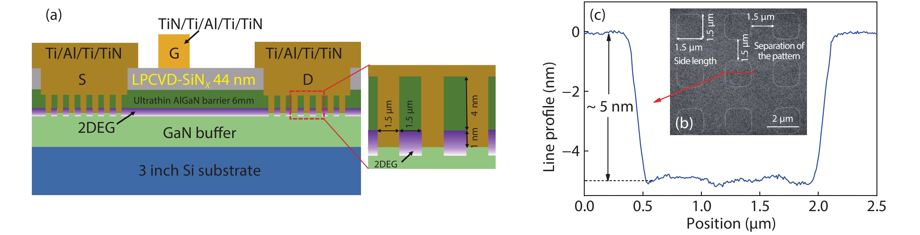
    Fig. 1. (Color online) (a) Schematic cross section of the fabricated Si-CMOS-compatible GaN MIS-HEMTs utilizing a micro-patterned ohmic recess. (b) SEM image. (c) Line profile of the micro-patterned AlGaN/GaN heterostructure measured by atomic force microscopy (AFM).
    (a) Linear fit of the fabricated Ti/Al/Ti/TiN ohmic contact resistances versus TLM spacing. (b) Temperature-dependent characteristics: RC and RSH. (c) ρC as fitted by thermionic field emission model. (d) Temperature-dependent transfer length LT.
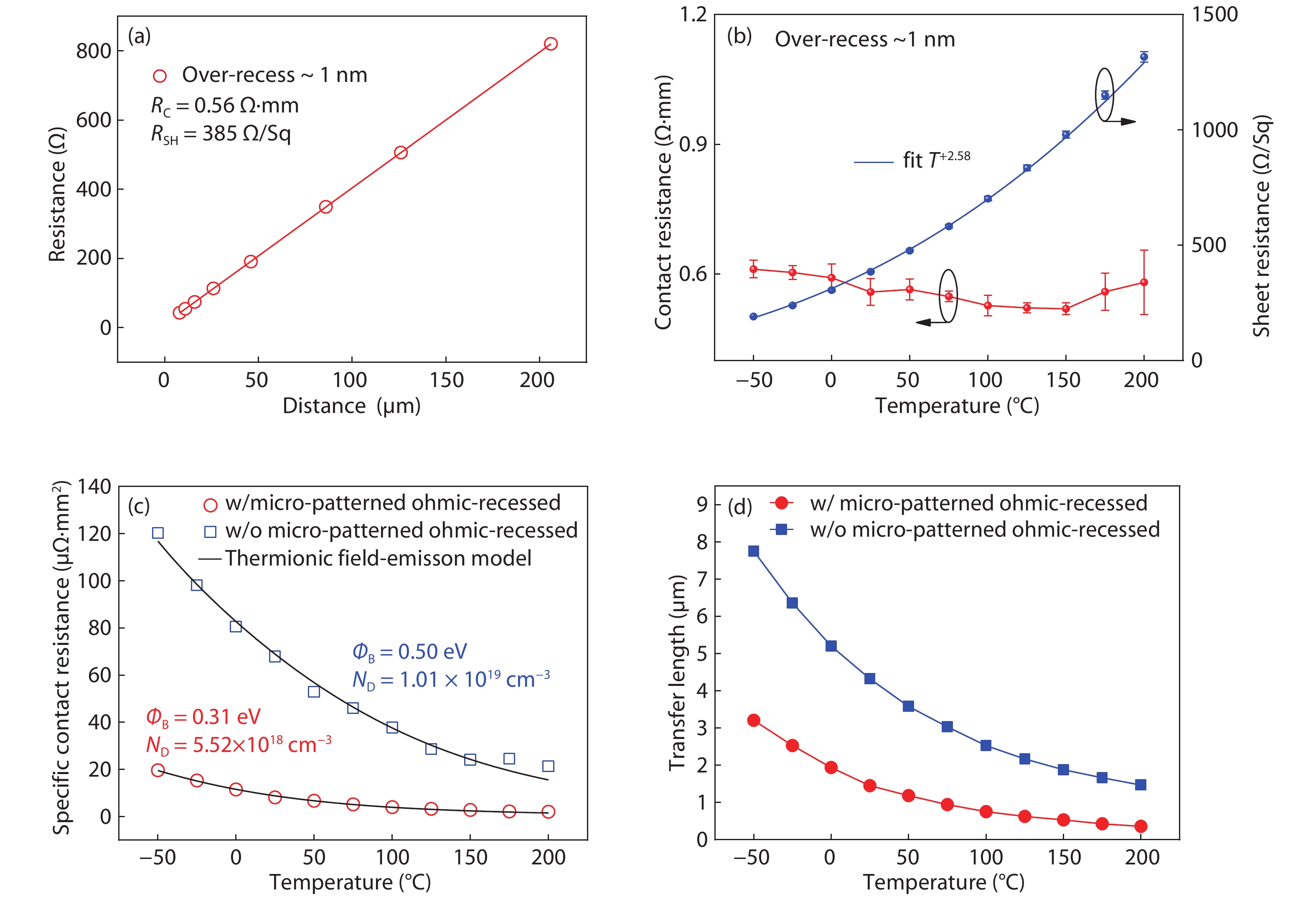
    Fig. 2. (a) Linear fit of the fabricated Ti/Al/Ti/TiN ohmic contact resistances versus TLM spacing. (b) Temperature-dependent characteristics: RC and RSH. (c) ρC as fitted by thermionic field emission model. (d) Temperature-dependent transfer length LT.
    (Color online) (a) DC output, (b) transfer, and (c) off-state leakage characteristics of the fabricated CMOS-process compatible LPCVD-SiNx/AlGaN/GaN MIS-HEMTs.
    Fig. 3. (Color online) (a) DC output, (b) transfer, and (c) off-state leakage characteristics of the fabricated CMOS-process compatible LPCVD-SiNx/AlGaN/GaN MIS-HEMTs.
    AlGaN/GaN heterostructureOhmic metal stackAnnealing temperature (°C)Recessed-AlGaN barrier thickness in the patterned region (nm) Side length / Separation of pattern (μm) LT (μm) RC (Ω·mm) RSH (Ω/sq)
    30 nm Al0.25Ga0.75N/GaN[24]TiSi2/TiN non-alloy55.00/10.0013.415.86437
    24 nm Al0.3Ga0.7N/GaN[17]Ti/Al/Ni/Au850150.50/0.500.350.12341
    2 nm GaN(cap)/18 nm Al0.26Ga0.74N/GaN[18]Ti/Al/Ni/Au790121.00/1.001.100.52475
    Ti/Al/Ni/Au810121.00/1.001.000.48475
    Ti/Al/Ni/Au790over-recess 301.00/1.001.060.51475
    Ti/Al/Ni/Au810over-recess 301.00/1.001.060.50475
    (UTB) 1 nm GaN(cap)/ 3 nm Al0.25Ga0.75N/ 1 nm AlN/GaN[16]Ti/Al/Ti/TiN6005/4.331.57363
    (UTB) 1 nm GaN(cap)/ 4 nm Al0.25Ga0.75N/ 1 nm AlN/GaN (This work) Ti/Al/Ti/TiN550over-recess ~11.50/1.501.450.56385
    over-recess ~101.50/1.501.450.58399
    Table 1. The summary of micro-patterned ohmic contacts to various AlGaN/GaN heterostructures.
    Wen Shi, Sen Huang, Xinhua Wang, Qimeng Jiang, Yixu Yao, Lan Bi, Yuchen Li, Kexin Deng, Jie Fan, Haibo Yin, Ke Wei, Yankui Li, Jingyuan Shi, Haojie Jiang, Junfeng Li, Xinyu Liu. Low-thermal-budget Au-free ohmic contact to an ultrathin barrier AlGaN/GaN heterostructure utilizing a micro-patterned ohmic recess[J]. Journal of Semiconductors, 2021, 42(9): 092801
    Download Citation