
Wen Shi, Sen Huang, Xinhua Wang, Qimeng Jiang, Yixu Yao, Lan Bi, Yuchen Li, Kexin Deng, Jie Fan, Haibo Yin, Ke Wei, Yankui Li, Jingyuan Shi, Haojie Jiang, Junfeng Li, Xinyu Liu. Low-thermal-budget Au-free ohmic contact to an ultrathin barrier AlGaN/GaN heterostructure utilizing a micro-patterned ohmic recess[J]. Journal of Semiconductors, 2021, 42(9): 092801
- Journal of Semiconductors
- Vol. 42, Issue 9, 092801 (2021)
Abstract
1. Introduction
The good potential of the ultrathin barrier (UTB) AlGaN/GaN heterostructure has been demonstrated in the fabrication of high uniformity GaN-on-Si power devices and integration of peripheral controlling circuits[
Regrowth of n-type GaN on source–drain region is an effective way to reduce Rc to 0.05–0.15 Ω·mm[
To break the RC limit of the uniform-ohmic-recess process, a patterned AlGaN layer structure was proposed on Ti/Al/Ni/Au ohmic contact to a conventional AlGaN/GaN heterostructure[
2. Device fabrication
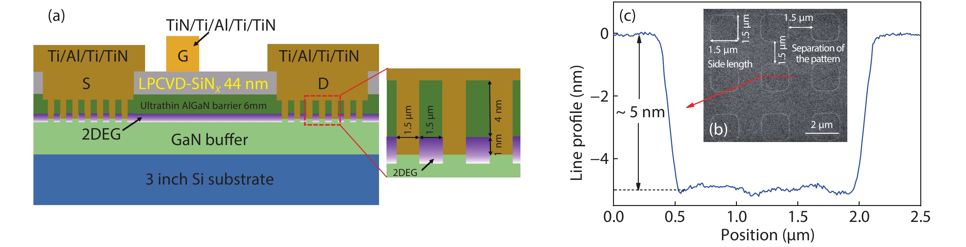
The schematic cross section of the fabricated CMOS-compatible LPCVD-SiNx/AlGaN/GaN MIS-HEMTs is depicted in Fig. 1(a). The UTB-AlGaN/GaN heterostructure wafer used in this work was grown by metal organic chemical vapor deposition (MOCVD) on a 3-inch Si substrate.
![]()
Figure 1.(Color online) (a) Schematic cross section of the fabricated Si-CMOS-compatible GaN MIS-HEMTs utilizing a micro-patterned ohmic recess. (b) SEM image. (c) Line profile of the micro-patterned AlGaN/GaN heterostructure measured by atomic force microscopy (AFM).
The AlGaN barrier consists of a ~1 nm GaN cap, a ~4 nm Al0.25Ga0.75N layer and a ~1 nm AlN interface enhancement layer. The fresh wafers were first cleaned by standard Radio Corporation of America (RCA) treatment, followed by a ~44 nm LPCVD-SiNx deposited immediately at 780 °C. The high deposition temperature ensures compact film quality and good thermal stability of the SiNx film, and moreover provides sufficient thermal budget for the subsequent process[
The Ti/Al/Ti/TiN ohmic metal stack was then sputtered to cover the ohmic contact region by another photolithography with a proper wet treatment of the etched surface. The source-drain ohmic contact was then annealed at 550 °C for 90 s in N2 ambient. Subsequently, a TiN/Ti/Al/Ti/TiN metal stack was sputtered over the LPCVD-SiNx layer to form a MIS-gated structure. The fabricated MIS-HEMTs were finally annealed at 280 °C for 4 min in N2 ambient to further improve the thermal stability of the gate. The gate length LG, gate-to-source LGS, and gate-to-drain distance LGS of the MIS-HEMTs are 2.25, 1.25, and 1.75 μm, respectively.
3. Results and discussion
The transmission line method (TLM) was used for the determination of RC and RSH for the Au-free ohmic contact utilizing a pre-ohmic micro-patterned recess process, as shown in Fig. 2(a). The typical RC of the Au-free ohmic contact is determined to be 0.56 Ω·mm, about one-third of our previous reported value (1.57 Ω·mm) without the micro-patterned ohmic recess[
![]()
Figure 2.(a) Linear fit of the fabricated Ti/Al/Ti/TiN ohmic contact resistances versus TLM spacing. (b) Temperature-dependent characteristics:
Temperature-dependent four-probe measurement was conducted from –50 to 200 °C, in an N2 protecting environment, to explore the contact mechanism of the fabricated Au-free ohmic contact (Fig. 2(b)). RC is observed to vary slightly over the temperature range, while RSH increases with the temperature. The latter is due to optical phonon scattering induced by degradation of 2-D electron gas (2DEG) mobility at high temperature (T > ~ 200 K) [
where
and
where A* = 4πm*kB2/h3 is the effective Richardson constant, m* is the effective mass of the tunneling electrons in (Al)GaN, ε is the dielectric constant of (Al)GaN, ФB is Schottky barrier height between (Al)GaN and the ohmic metals, ND is electron carrier concentration, and En is the energy difference between the conduction-band edge and the Fermi level at the AlGaN/GaN interface.
As for the patterned ohmic contact, the TFE fitting yields a Schottky barrier height ФB of 0.31 eV and a ND of 5.5 × 1018 cm–3, in contrast to the value of 0.50 eV and 1.01 × 1019 cm–3 obtained in the un-patterned sample. The lower ФB is due to partial transition of metal/AlGaN to metal/GaN contact because of over-etching of the AlGaN barrier. However, over-etching also results in 2DEG depletion in the micro-patterned region, giving rise to a reduced ND. Further investigation is ongoing to verify the trade-off between ФB and ND and their effects on ρc. Transfer length LT of the fabricated ohmic contacts have also been plotted in Fig. 2(d) with the temperature. The micro-pattern ohmic recess leads to a remarkable reduction of LT in the measured range. And the shorter current flow distance from the metal (semiconductor) to the semiconductor (metal) can be attributed to the larger lateral contact area to collect current.
To shed light on the effect of pattern size on the contact resistance, a survey of state-of-the-art ohmic contacts that adopts a similar pre-ohmic pattern process is summarized in Table 1. It can be observed that whether the AlGaN barrier in the patterned region is partially or fully recessed, the change of LT follows closely with the pattern separation. For instance, LT decreases from 1.45 to 0.35 μm as the separation is reduced from 1.50 (this work) to 0.50 μm[
The pre-ohmic micro-pattered recess process was then implemented in a fabrication of CMOS-compatible LPCVD-SiNx/AlGaN/GaN MIS-HEMTs, with LPCVD-SiNx serving as the gate dielectric. The MIS-HEMTs’ output characteristics are shown in Fig. 3(a). The on-state resistance (RON), as extracted from the linear region of the output curve, composed of ohmic contact resistance 2RC (22.89%), access region resistance Rs + Rd (23.62%) and gate channel resistance RChannel (53.49%), is substantially low owing to the ohmic pattern process. High ON/OFF current ratios (ION/IOFF) are more than 9 × 10¹⁰ while low gate leakage (~10–7 mA/mm) is also obtained in transfer measurements (Fig. 3(b)), thanks to the high insulating behavior of the LPCVD-SiNx gate dielectric. Due to the trapping behavior of deep states located at the LPCVD-SiNx/GaN interface, a clockwise threshold voltage (VTH) hysteresis of 0.23 V is observed at a drain bias of 1 V (Fig. 3(b)). A smaller VTH hysteresis, while a relative lower extrinsic transconductance, can be further realized with proper surface treatments[
![]()
Figure 3.(Color online) (a) DC output, (b) transfer, and (c) off-state leakage characteristics of the fabricated CMOS-process compatible LPCVD-SiN
4. Conclusion
A pre-ohmic micro-patterned recess process was developed to facilitate low-thermal-budget Au-free ohmic contact to a UTB-AlGaN/GaN heterostructure. The contact mechanism of ohmic-patterned technology on a UTB AlGaN/GaN heterostructure and the relationship between LT and pattern size were revealed. CMOS-process-compatible SiNx/AlGaN/GaN MIS-HEMTs were fabricated with the proposed Au-free ohmic contact and LPCVD-SiNx gate dielectric.
Acknowledgements
This work was supported by National Natural Science Foundation of China under Grant 61822407, Grant 62074161, and Grant 11634002; in part by the Key Research Program of Frontier Sciences, Chinese Academy of Sciences (CAS) under Grant QYZDB-SSW-JSC012; in part by the National Key Research and Development Program of China under Grant 2016YFB0400105 and Grant 2017YFB0403000; in part by the Youth Innovation Promotion Association of CAS; in part by the University of Chinese Academy of Sciences; and in part by the Opening Project of Key Laboratory of Microelectronic Devices & Integrated Technology, Institute of Microelectronics, CAS.
References
[1] S Huang, X Y Liu, X H Wang et al. Ultrathin-barrier AlGaN/GaN heterostructure: A recess-free technology for manufacturing high-performance GaN-on-Si power devices. IEEE Trans Electron Devices, 65, 207(2018).
[2] H X Jiang, C W Tang, K M Lau. Enhancement-mode GaN MOS-HEMTs with recess-free barrier engineering and high-k ZrO2 gate dielectric. IEEE Electron Device Lett, 39, 405(2018).
[3] P C Han, Z Z Yan, C H Wu et al. Recess-free normally-off GaN MIS-HEMT fabricated on ultra-thin-barrier AlGaN/GaN heterostructure. 2019 31st International Symposium on Power Semiconductor Devices and ICs (ISPSD), 427(2019).
[4] S Huang, X H Wang, X Y Liu et al. Monolithic integration of E/D-mode GaN MIS-HEMTs on ultrathin-barrier AlGaN/GaN heterostructure on Si substrates. Appl Phys Express, 12, 024001(2019).
[5]
[6]
[7] D Marcon, B De Jaeger, S Halder et al. Manufacturing challenges of GaN-on-Si HEMTs in a 200 mm CMOS fab. IEEE Trans Semicond Manuf, 26, 361(2013).
[8] H S Lee, D S Lee, T Palacios. AlGaN/GaN high-electron-mobility transistors fabricated through a Au-free technology. IEEE Electron Device Lett, 32, 623(2011).
[9] Y Li, G I Ng, S Arulkumaran et al. Conduction mechanism of non-gold Ta/Si/Ti/Al/Ni/Ta ohmic contacts in AlGaN/GaN high-electron-mobility transistors. Appl Phys Express, 8, 041001(2015).
[10] J H Zhang, S Huang, Q L Bao et al. Mechanism of Ti/Al/Ti/W Au-free ohmic contacts to AlGaN/GaN heterostructures via pre-ohmic recess etching and low temperature annealing. Appl Phys Lett, 107, 262109(2015).
[11] A Shriki, R Winter, Y Calahorra et al. Formation mechanism of gold-based and gold-free ohmic contacts to AlGaN/GaN heterostructure field effect transistors. J Appl Phys, 121, 065301(2017).
[12] T Yoshida, T Egawa. Improvement of Au-free, Ti/Al/W ohmic contact on AlGaN/GaN heterostructure featuring a thin-Ti layer and low temperature annealing. Phys Status Solidi A, 215, 1700825(2018).
[13] J H Zhang, X W Kang, X H Wang et al. Ultralow-contact-resistance Au-free ohmic contacts with low annealing temperature on AlGaN/GaN heterostructures. IEEE Electron Device Lett, 39, 847(2018).
[14] M Y Fan, G Y Yang, G N Zhou et al. Ultra-low contact resistivity of < 0.1 Ω mm for Au-free Ti
[15] X H Ma, Y Liu, X H Wang et al. Effect of alloying temperature on the capacitance-voltage and current-voltage characteristics of low-pressure chemical vapor deposition SiN
[16] Y K Wang, S Huang, X H Wang et al. Effects of fluorine plasma treatment on Au-free ohmic contacts to ultrathin-barrier AlGaN/GaN heterostructure. IEEE Trans Electron Devices, 66, 2932(2019).
[17] J Guo, G W Li, F Faria et al. MBE-regrown ohmics in InAlN HEMTs with a regrowth interface resistance of 0.05 Ω mm. IEEE Electron Device Lett, 33, 525(2012).
[18] T D Huang, X L Zhu, K M Lau. Enhancement-mode AlN/GaN MOSHFETs on Si substrate with regrown source/drain by MOCVD. IEEE Electron Device Lett, 33, 1123(2012).
[19] H J Yu, L McCarthy, S Rajan et al. Ion implanted AlGaN-GaN HEMTs with nonalloyed Ohmic contacts. IEEE Electron Device Lett, 26, 283(2005).
[20] Y Lu, X H Ma, L Yang et al. High RF performance AlGaN/GaN HEMT fabricated by recess-arrayed ohmic contact technology. IEEE Electron Device Lett, 39, 811(2018).
[21] B Benakaprasad, A M Eblabla, X Li et al. Optimization of ohmic contact for AlGaN/GaN HEMT on low-resistivity silicon. IEEE Trans Electron Devices, 67, 863(2020).
[22] J Antoszewski, M Gracey, J M Dell et al. Scattering mechanisms limiting two-dimensional electron gas mobility in Al0.25Ga0.75N/GaN modulation-doped field-effect transistors. J Appl Phys, 87, 3900(2000).
[23] Z H Liu, S Arulkumaran, G I Ng. Temperature dependence of Ohmic contact characteristics in AlGaN/GaN high electron mobility transistors from −50 to 200 °C. Appl Phys Lett, 94, 142105(2009).
[24] A Aminbeidokhti, S Dimitrijev, J S Han et al. The power law of phonon-limited electron mobility in the 2-D electron gas of AlGaN/GaN heterostructure. IEEE Trans Electron Devices, 63, 2214(2016).
[25] F Iucolano, G Greco, F Roccaforte. Correlation between microstructure and temperature dependent electrical behavior of annealed Ti/Al/Ni/Au Ohmic contacts to AlGaN/GaN heterostructures. Appl Phys Lett, 103, 201604(2013).
[26] F Iucolano, F Roccaforte, A Alberti et al. Temperature dependence of the specific resistance in Ti/Al/Ni/Au contacts on n-type GaN. J Appl Phys, 100, 123706(2006).
[27] Y Takei, M Kamiya, K Tsutsui et al. Reduction of contact resistance on AlGaN/GaN HEMT structures introducing uneven AlGaN layers. Phys Status Solidi A, 212, 1104(2015).


Set citation alerts for the article
Please enter your email address

© Copyright 2018-2021 | Chinese Laser Press. All Rights Reserved 沪ICP备15018463号-20