
C. Usha, P. Vimala. A compact two-dimensional analytical model of the electrical characteristics of a triple-material double-gate tunneling FET structure[J]. Journal of Semiconductors, 2019, 40(12): 122901
- Journal of Semiconductors
- Vol. 40, Issue 12, 122901 (2019)
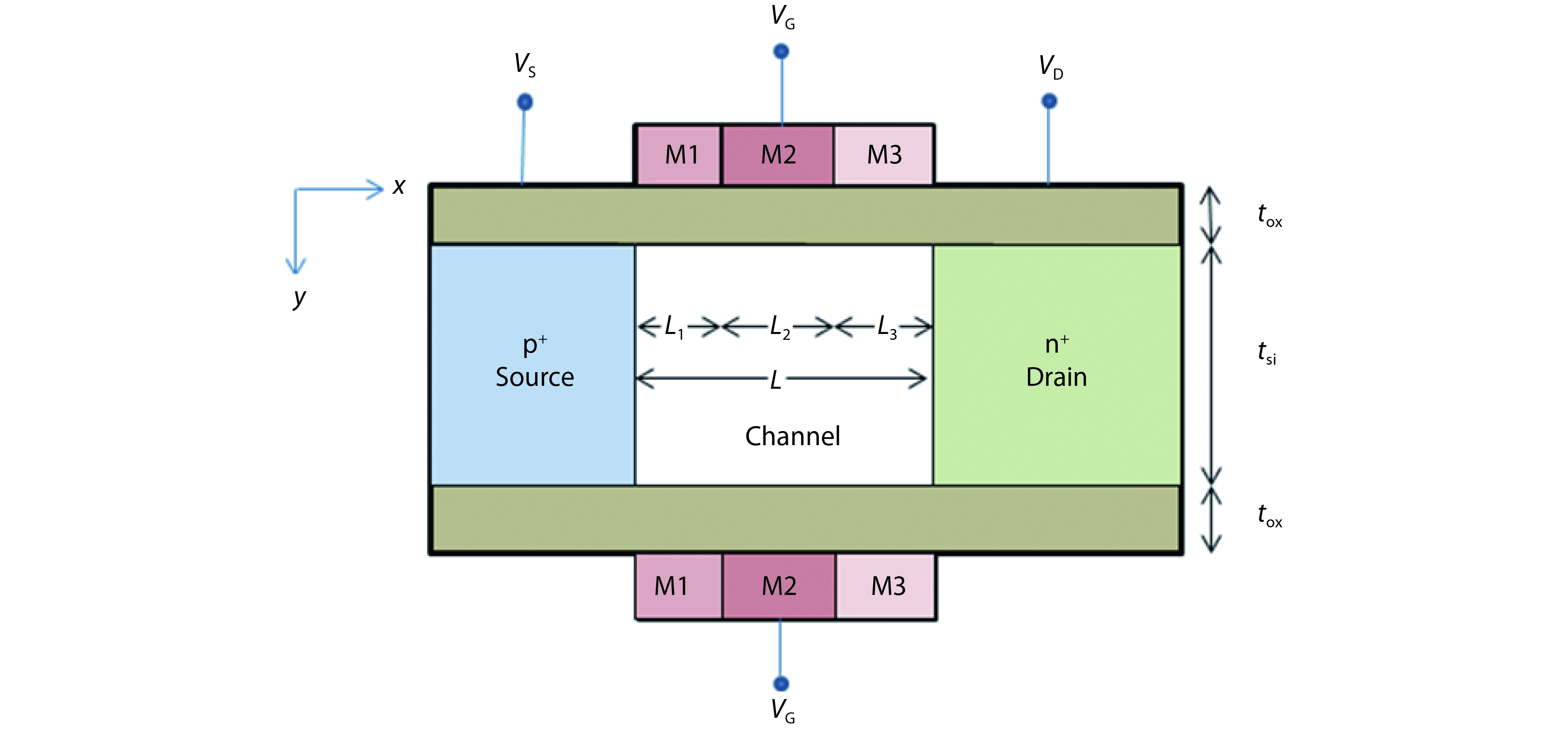
Fig. 1. (Color online) Schematic diagram of triple metal double-gate TFET (n-type).
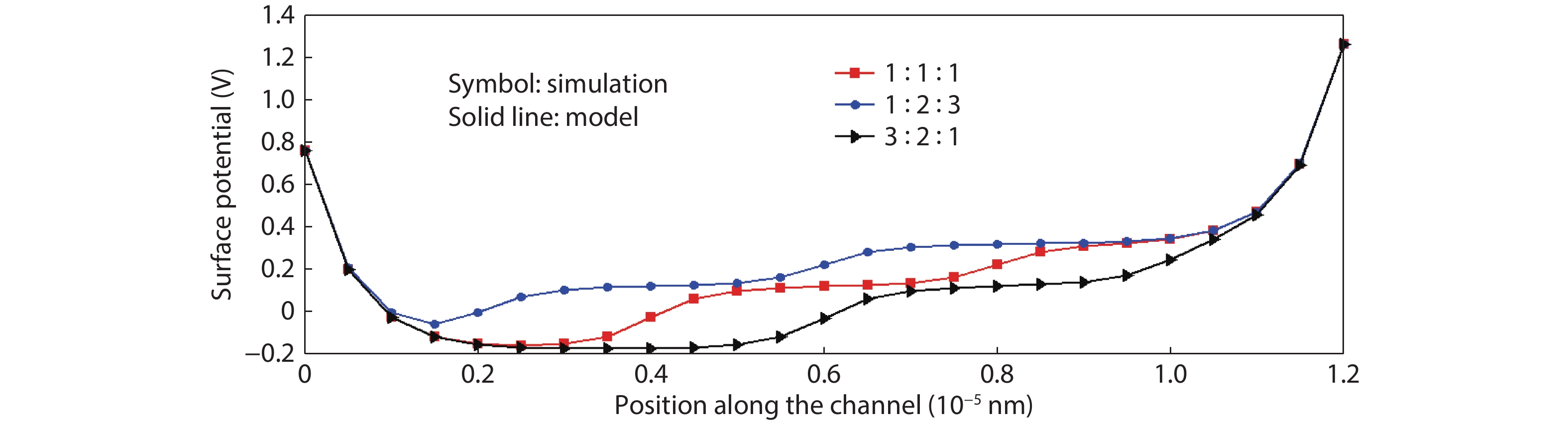
Fig. 2. (Color online) Surface potential variation along the position of channel from the p-type doped source to n-type doped drain with different L 1 : L 2 : L 3 ratio for V GS = 0.25 V, V DS = 0.5 V, and t ox = 2 nm.
Fig. 3. (Color online) Lateral electric field along the position of channel from the p- type doped source to the n- type doped drain with different L 1 : L 2 : L 3 ratio for V GS = 0.25 V, V DS = 0.5 V, and t ox = 2 nm.
Fig. 4. (Color online) Surface potential across channel length L = 120 nm and V GS = 0.25 V with different V DS = 0.25, 0.5, and 1 V.
Fig. 5. (Color online) Lateral electric field across the channel length L = 120 nm, V GS = 0.25 V for different V DS = 0.25, 0.5 and 1 V.
Fig. 6. (Color online) Surface potential along the channel with length L = 120 nm and V DS = 0.5 V for different V GS = 0.2, 0.4, and 0.6 V.
Fig. 7. (Color online) Lateral electric field profile for channel length L = 120 nm and V DS = 0.5 V for different gate voltages.
Fig. 8. (Color online) Vertical electric field along the channel for V GS = 0.25 V, V DS = 0.5 V, and t ox = 2 nm.
Fig. 9. (Color online) I d–V GS characteristics on a linear scale for V DS = 0.5 V and t si = 5 nm for different oxide thickness.
Fig. 10. (Color online) I d–V GS characteristics on a linear scale for V DS = 0.5 V and t ox = 2 nm for different channel thickness.
Fig. 11. (Color online) I d–V GS characteristics on a linear scale for V DS = 0.5 V and for a three different metal work function.

Set citation alerts for the article
Please enter your email address
© Copyright 2018-2021 | Chinese Laser Press. All Rights Reserved 沪ICP备15018463号-20