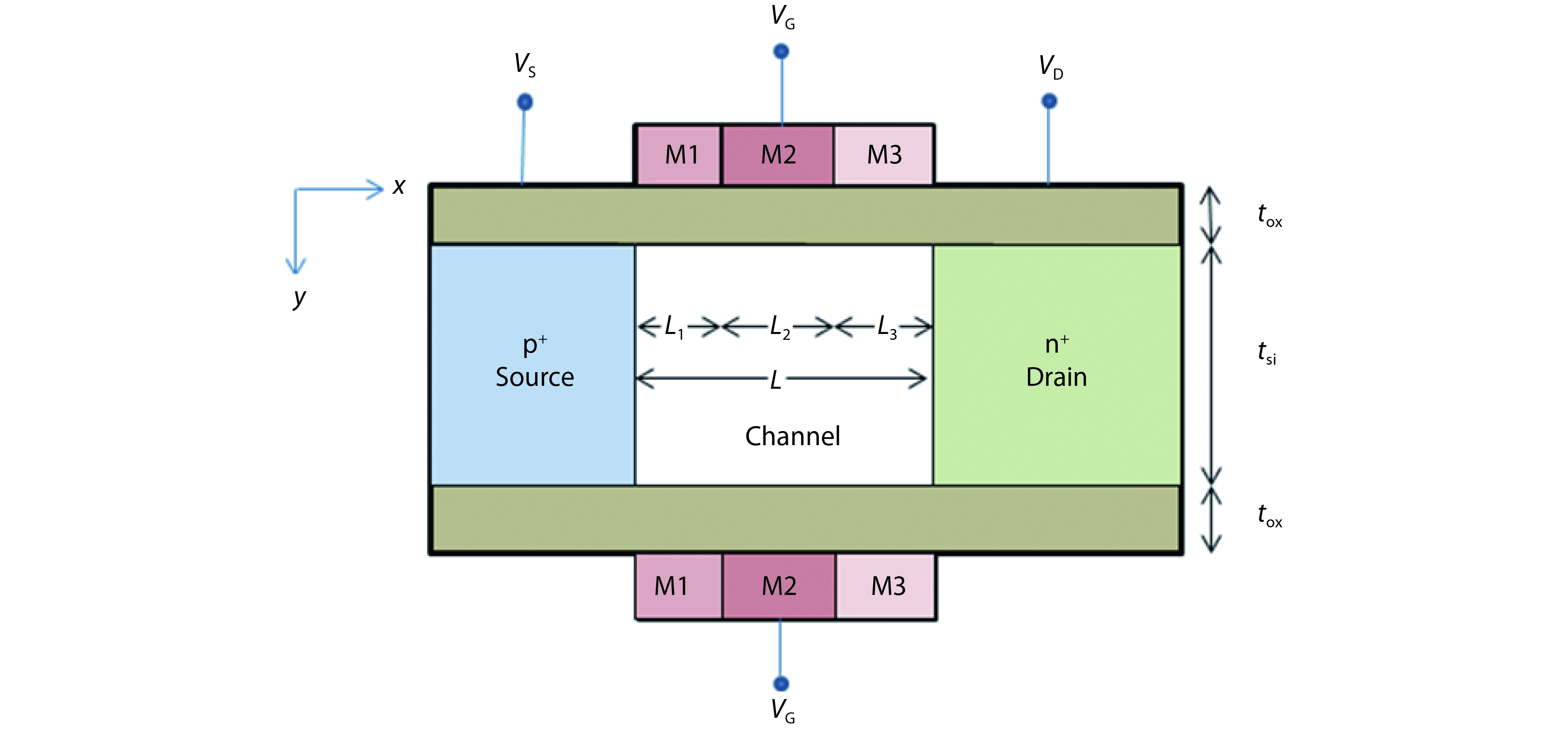
[1] E H Toh, G H Wang, G Samudra et al. Device physics and design of germanium tunneling field-effect transistor with source and drain engineering for low power and high performance applications. J Appl Phys, 103, 104504(2008).
[2] S O Koswatta, M S Lundstrom, S E Nikonov et al. Performance comparison between p–i–n tunneling transistors and conventional MOSFETs. IEEE Trans Electron Devices, 56, 456(2009).
[3] A C Seabaugh, Q Zhang. Low-voltage tunnel transistors for beyond CMOS logic. Proc IEEE, 98, 2095(2010).
[4] S Saurabh, M J Kumar. Novel attributes of a dual material gate nanoscale tunnel field-effect transistor. IEEE Trans Electron Devices, 58, 404(2011).
[5] E Gnani, A Gnudi, S Reggiani et al. Drain-conductance optimization in nanowire TFETs by means of a physics-based analytical model. Solid-State Electron, 84, 96(2013).
[6] K Boucart, A M Ionescu. A new definition of threshold voltage in tunnel FETs. Solid State Electron, 52, 1318(2008).
[7] W Vandenberghe, A Verhulst, G Greseneken et al. Analytical model for tunnel field- effect transistor. Proc MELECON, 923(2008).
[8] N N Mojunder, K Roy. Band-to-Band tunneling ballistic low-power digital circuits and memories. IEEE Trans Electron Devices, 56, 2193(2009).
[9] W Vandenberghe, A Verhulst, G Greseneken et al. Analytical model for point and line tunneling in a tunnel field-effect transistor. Proc Int Conf SISPAD, 137(2008).
[10] M G Bardon, H P Neves, R Puerd et al. Pseudo-two dimensional model for double gate tunnel FETs considering the junctions depletion regions. IEEE Trans Electron Devices, 57, 827(2010).
[11] L Liu, D Mohata, S Datta. Scaling length theory of double-gate interband tunnel field-effect transistors. IEEE Trans Electron Devices, 59, 902(2012).
[12] M J Lee, W Y Choi. Analytical model of single-gate silicon on insulator tunneling field effect tansistors (TFETs). Solid State Electron, 63, 110(2011).
[13] L Zhang, X Lin, J He et al. Analytical charge model for double gate tunnel FETs. IEEE Trans Electron Devices, 59, 3217(2012).
[14] A Pan, C O Chui. A quasi-analytical model for double-gate tunneling field effect transistors. IEEE Trans Electron Devices, 33, 1468(2012).
[15] B Bhushan, K Nayak, V R Rao. DC compact model for SOI tunnel field-effect tansistors. IEEE Trans Electron Devices, 59, 2635(2012).
[16] A S Verhulst, D Leoneli, R Rooyackers et al. Drain voltage dependent analytical model of tunnel field-effect transistor. J Appl Phys, 110, 024510(2011).
[17] V Dobrovolsky, F Sizov. Analytical model of the thin-film silicon-on-insulator tunneling field effect transistor. J App Phys, 110, 114513(2011).
[18] J Wan, C L Royer, A Zaslavsky et al. A tunneling field effect transistor model conbining interband tunneling with channel transport. J Appl Phys, 110, 104503(2011).
[19] R Vishnoi, M J Kumar. Compact analytical model of dual material gate tunneling field-effect transistor using interband tunneling and channel transport. IEEE Trans Electron Devices, 61, 1936(2014).
[20] T S A Samuel, N B Balamurugan. An analytical modeling and simulation of dual material double gate tunnel field effect transistor for low power applications. J. Elect Eng Technol, 9, 247(2014).
[21] R Vishnoi, M J Kumar. 2-D analytical model for the threshold voltage of a tunneling FET with localized charges. IEEE Trans Electron Devices, 61, 3054(2014).
[22] P Pandey, R Vishnoi, M J Kumar. A full-range dual material gate tunnel field effect transistor drain current model considering both source and drain depletion region band-to-band tunneling. J Comput Electron, 14, 280(2014).
[23] L Zhang, M Chan. SPICE modelling of double-gate tunnel-FETs including channel transports. IEEE Trans Electron Devices, 61, 300(2014).
[24] R Vishnoi, M J Kumar. An accurate compact analytical model for the drain current of a TFET from subthreshold to strong inversion. IEEE Trans Electron Devices, 62, 478(2015).
[25] S Dash, G P Mishra. A two-dimensional analytical cylindrical gate tunnel FET (CG-TFET) model: Impact of shortest tunneling distance. Adv Natural Sci, Nanosci Nanotechnol, 6, 035005(2015).
[26] N Bagga, S K Sarkar. An analytical model for tunnel barrier modulation in triple metal double gate TFET. IEEE Trans Electron Devices, 62, 2136(2015).
[27] S Dash, G P Mishra. A new analytical threshold voltage model of cylindrical gate tunnel FET (CG-TFET). Superlattices Microstruct, 86, 211(2015).
[28] S L Noor, S Safa, M Z R Khan. Dual-material double-gate tunnel FET: Gate threshold voltage modeling and extraction. J Comput Electron, 15, 763(2016).


