
C. Usha, P. Vimala. A compact two-dimensional analytical model of the electrical characteristics of a triple-material double-gate tunneling FET structure[J]. Journal of Semiconductors, 2019, 40(12): 122901
- Journal of Semiconductors
- Vol. 40, Issue 12, 122901 (2019)
Abstract
1. Introduction
Over the past few decades, the performance of metal–oxide–semiconductor field-effect transistors (MOSFETs) has greatly improved thanks to their incessant and aggressive scaling. CMOS transistors scaling exhibits several short channel effects (SCEs). The short channel effects in MOSFETs are drain induced barrier lowering (DIBL), high leakage currents during OFF-state, high subthreshold slope (SS) and others. These effects lead to greater static power consumption and evil switching characteristics. Hence, substitute, innovative devices are introduced, among which tunneling field-effect transistor (TFET) is a promising candidate[
Numerous analytical models are carried out in the literature[
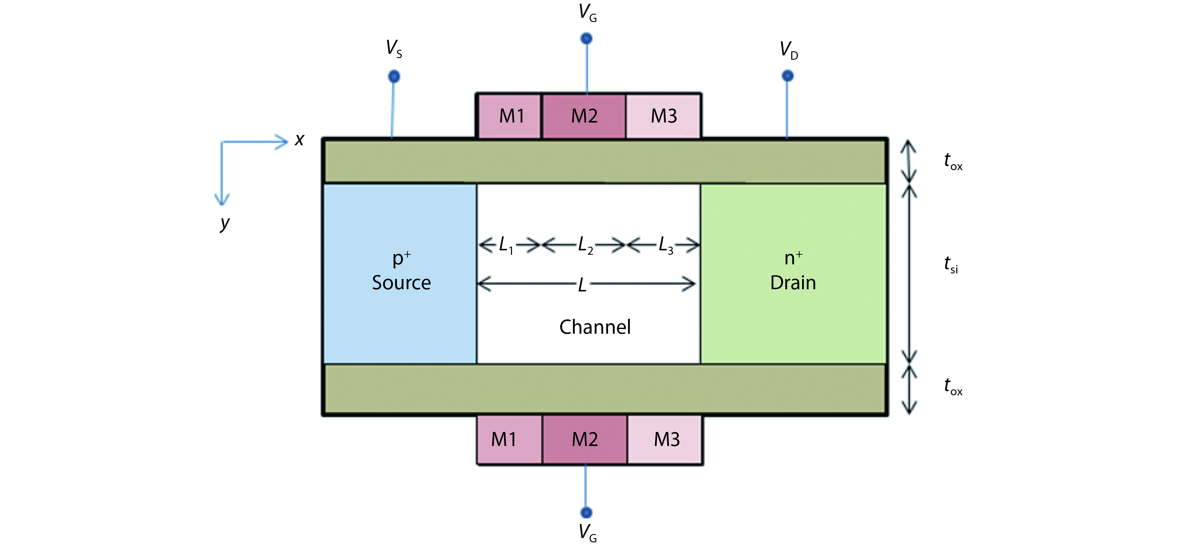
2. Device parameters and structure
The schematic of a triple-material double-gate tunneling FET shown in Fig. 1, where M1, M2 and M3 are three different metals having different work function: Cobalt(ϕm1 = 5 eV), Iron(ϕm2 = 4.7 eV) and Chromium(ϕm3 = 4.5 eV) in the channel region. Both the back and front gates consists of three metals, with each channel length having L1, L2 and L3. The drain is n-type doped, the source is p-type doped, and the channel section is lightly doped with n-type. The effect of oxide charges is neglected because the channel is uniformly doped. tsi and tox are the thickness of channel and the oxide.
![]()
Figure 1.(Color online) Schematic diagram of triple metal double-gate TFET (n-type).
The OFF-state current is quite low due to reduced work function ϕm and on source side there is no band overlap. The probability of tunneling of carriers on the source side increases because the band overlap increases as the tunneling width decreases. Hence, electrons tunnel from valence band to the conduction band of source in the intrinsic body and they then drift to drain by a process of drift diffusion. If there is an increase in ϕm, then the band diagram in ON-state does not change.
3. Analytical model
3.1. Surface potential
The potential distribution in the oxide region of the gate is distinguished by using a two-dimensional Poisson’s equation:
The parabolic approximation approach is employed to resolve the two-dimensional Poisson’s equation for TMDG TFET. The parabolic method is used to calculate the potential distribution over the two-dimensional space (along device depth and device length) and an equation for the potential is given as follows
C0(x), C1(x) and C2(x) are arbitrary constants, each constant is functions of x. Since the gate consists of three materials, the potential under each material M1, M2 and M3 are given in Eqs. (3)–(5), respectively
The boundary conditions required for the solution of Poisson’s equation are as follows.
3.1.1. At the front-oxide gate interface, the electric flux is continuous in TMDG TFET, as given in Eqs. (6)–(8)
3.1.2. At the back gate-oxide and the back channel interface the electric flux is continuous in three materials and it is given in Eqs. (9)–(11) as follows
By applying the above boundary condition from Eq. (6) to Eq. (11) we obtain
3.1.3. The potential equations across source end and drain end are as follows
By applying these boundary conditions, the calculated surface potential
where
Eg is the energy bandgap, Vgs is the gate voltage, q is elementary charge, VDS is the drain to source voltage, Vbi is the built in potential, εsi and εox is the relative permittivity of silicon and silicon dioxide, L is channel length, χ is electron affinity and ϕm is work function of metal. Solving the Eqs. (27)–(29) we obtain A, B, C, D, E and F.
3.2. Electric field
The lateral electric field Ex and vertical electric field Ey are found by deriving potential with respect to x andy, respectively. The lateral electric field is given in Eqs. (36)–(38) as
The vertical electric field is given in Eqs. (39)–(41) as
3.3. Drain current
The current in TMDG TFET depends on the BTBT of electrons from source valance band to conduction band of channel region, which is given as
where generation rate (G) can be calculated using Kane’s model which is given as
where A1 = 4 × 1014 cm–1/2V–5/2s–1 and B1 = 1.9 × 10⁷ V/cm are the Kane’s parameters, E the magnitude of the electric field which is defined as
4. Results and discussion
Our proposed models are verified using two-dimensional numerical simulation. Fig. 1 gives a cross-sectional view of the proposed model TM-DG TFET, in which both front and back gates are composed of three materials with three various work functions. Fig. 2 provides the plot of surface potential versus position along the channel, for TM-DG TFET with different combinations channel length ratios, such as 1 : 1 : 1, 3 : 2 : 1 and 1 : 2 : 3 for a total channel length; i.e., L = 120 nm, VGS = 0.25, VDS = 0.5 and tox = 2 nm, respectively. The TM-DG TFET potential graph provides enhanced screening of channel space with respect to the first metal to be depleted from potential variation. The 3 : 2 : 1 device model needs high vitality to provide higher potential boundary as compared with other structures, with an increase in power supply to a substantial threshold voltage. In addition, the movement of carriers is decreased due to substantial potential barrier at the source side. The 1 : 2 : 3 device model outshines because of its enhanced carrier transport effectiveness.
![]()
Figure 2.(Color online) Surface potential variation along the position of channel from the p-type doped source to n-type doped drain with different
Fig. 3 demonstrates the correlations of lateral electric field across the channel for TM-DG TFET structures for Vgs = 0.25, Vds = 0.5 and tox = 2 nm. The two peaks obtained in the electric field profile of TMDG structure indicate appropriate carrier transport efficiency and an appropriate average electric field along the channel. The extra peak in electric field increases the speed of the carriers in the channel, along these lines guaranteeing a vertical extent gate transport effectiveness to provide more quantities of carriers to drain. In addition, at the drain side a reduced peak of electric field appeared to offer an extra advantage of giving higher resistance to HCEs. Among the different TM-DG structures, TM-DG TFET (1 : 2 : 3) lateral electric field has a peak that is closest to the region of source, consequently guaranteeing a peak in its carrier’s speed closest to the source. This brings about the extreme refinement in the carrier transport effectiveness, influential transconductance, and higher drain current.
![]()
Figure 3.(Color online) Lateral electric field along the position of channel from the p- type doped source to the n- type doped drain with different
Fig. 4 shows surface potential variation versus position across the channel with Vgs constant, for different drain to source voltages (Vds). The potential increases only under third metal (M3) and no change under metal M1 and M2, as Vds increases. The lateral electric field variation for different Vds with constant Vgs shows a change in the drain side, which is shown in Fig.5. Fig. 6 shows the surface potential variation for different gate to source voltages (Vgs), while the Vds constant changes the surface potential throughout the channel. A variation of the lateral electric field along the channel length for different gate to source (Vgs) with constant Vds shows that there is a change in both source and drain side, as displayed in Fig. 7. The region under Metal 1 is reduced because the electric field is high at the source channel junction, which reduces the tunneling path. Fig. 8 shows the vertical electric field along the channel with VGS = 0.25 V, VDS= 0.5 V, and tox = 2 nm. The vertical electric field has ae peak when the work function of the metal varies. The first peak is obtained when carriers transfer from M1 to M2 and second peak is obtained from M2 to M3.
![]()
Figure 4.(Color online) Surface potential across channel length
![]()
Figure 5.(Color online) Lateral electric field across the channel length
![]()
Figure 6.(Color online) Surface potential along the channel with length
![]()
Figure 7.(Color online) Lateral electric field profile for channel length
![]()
Figure 8.(Color online) Vertical electric field along the channel for
The Id–VGS characteristic for different oxide thickness is shown in Fig. 9. To obtain a high ON–OFF current ratio, Fig. 10 shows variation of Id–VGS characteristic for different body thicknesses. A reduction in the body thickness helps to increase the current of the TFET, due to which the tunneling path is reduced with an exponential increase in tunneling probability. The Id–VGS characteristics for different work function combination are shown in Fig. 11. The tunneling current increases when the work function of M1 increases.
![]()
Figure 9.(Color online)
![]()
Figure 10.(Color online)
![]()
Figure 11.(Color online)
5. Conclusion
This paper proposes analytical modeling of a triple-material double-gate TFET. The tunneling path is modulated by the carriers over the channel due to the different work functions of the metals. The TM-DG TFET provides the better carrier transport efficiency, has higher resistance to HCEs, and obtains a high ON-OFF current ratio. Hence, TFET is strong promising behavior device that can be used in low-power applications.
Acknowledgement
This work was supported by Women Scientist Scheme-A, Department of Science and Technology, New Delhi, Government of India, under the Grant SR/WOS-A/ET-5/2017.
References
[1] E H Toh, G H Wang, G Samudra et al. Device physics and design of germanium tunneling field-effect transistor with source and drain engineering for low power and high performance applications. J Appl Phys, 103, 104504(2008).
[2] S O Koswatta, M S Lundstrom, S E Nikonov et al. Performance comparison between p–i–n tunneling transistors and conventional MOSFETs. IEEE Trans Electron Devices, 56, 456(2009).
[3] A C Seabaugh, Q Zhang. Low-voltage tunnel transistors for beyond CMOS logic. Proc IEEE, 98, 2095(2010).
[4] S Saurabh, M J Kumar. Novel attributes of a dual material gate nanoscale tunnel field-effect transistor. IEEE Trans Electron Devices, 58, 404(2011).
[5] E Gnani, A Gnudi, S Reggiani et al. Drain-conductance optimization in nanowire TFETs by means of a physics-based analytical model. Solid-State Electron, 84, 96(2013).
[6] K Boucart, A M Ionescu. A new definition of threshold voltage in tunnel FETs. Solid State Electron, 52, 1318(2008).
[7] W Vandenberghe, A Verhulst, G Greseneken et al. Analytical model for tunnel field- effect transistor. Proc MELECON, 923(2008).
[8] N N Mojunder, K Roy. Band-to-Band tunneling ballistic low-power digital circuits and memories. IEEE Trans Electron Devices, 56, 2193(2009).
[9] W Vandenberghe, A Verhulst, G Greseneken et al. Analytical model for point and line tunneling in a tunnel field-effect transistor. Proc Int Conf SISPAD, 137(2008).
[10] M G Bardon, H P Neves, R Puerd et al. Pseudo-two dimensional model for double gate tunnel FETs considering the junctions depletion regions. IEEE Trans Electron Devices, 57, 827(2010).
[11] L Liu, D Mohata, S Datta. Scaling length theory of double-gate interband tunnel field-effect transistors. IEEE Trans Electron Devices, 59, 902(2012).
[12] M J Lee, W Y Choi. Analytical model of single-gate silicon on insulator tunneling field effect tansistors (TFETs). Solid State Electron, 63, 110(2011).
[13] L Zhang, X Lin, J He et al. Analytical charge model for double gate tunnel FETs. IEEE Trans Electron Devices, 59, 3217(2012).
[14] A Pan, C O Chui. A quasi-analytical model for double-gate tunneling field effect transistors. IEEE Trans Electron Devices, 33, 1468(2012).
[15] B Bhushan, K Nayak, V R Rao. DC compact model for SOI tunnel field-effect tansistors. IEEE Trans Electron Devices, 59, 2635(2012).
[16] A S Verhulst, D Leoneli, R Rooyackers et al. Drain voltage dependent analytical model of tunnel field-effect transistor. J Appl Phys, 110, 024510(2011).
[17] V Dobrovolsky, F Sizov. Analytical model of the thin-film silicon-on-insulator tunneling field effect transistor. J App Phys, 110, 114513(2011).
[18] J Wan, C L Royer, A Zaslavsky et al. A tunneling field effect transistor model conbining interband tunneling with channel transport. J Appl Phys, 110, 104503(2011).
[19] R Vishnoi, M J Kumar. Compact analytical model of dual material gate tunneling field-effect transistor using interband tunneling and channel transport. IEEE Trans Electron Devices, 61, 1936(2014).
[20] T S A Samuel, N B Balamurugan. An analytical modeling and simulation of dual material double gate tunnel field effect transistor for low power applications. J. Elect Eng Technol, 9, 247(2014).
[21] R Vishnoi, M J Kumar. 2-D analytical model for the threshold voltage of a tunneling FET with localized charges. IEEE Trans Electron Devices, 61, 3054(2014).
[22] P Pandey, R Vishnoi, M J Kumar. A full-range dual material gate tunnel field effect transistor drain current model considering both source and drain depletion region band-to-band tunneling. J Comput Electron, 14, 280(2014).
[23] L Zhang, M Chan. SPICE modelling of double-gate tunnel-FETs including channel transports. IEEE Trans Electron Devices, 61, 300(2014).
[24] R Vishnoi, M J Kumar. An accurate compact analytical model for the drain current of a TFET from subthreshold to strong inversion. IEEE Trans Electron Devices, 62, 478(2015).
[25] S Dash, G P Mishra. A two-dimensional analytical cylindrical gate tunnel FET (CG-TFET) model: Impact of shortest tunneling distance. Adv Natural Sci, Nanosci Nanotechnol, 6, 035005(2015).
[26] N Bagga, S K Sarkar. An analytical model for tunnel barrier modulation in triple metal double gate TFET. IEEE Trans Electron Devices, 62, 2136(2015).
[27] S Dash, G P Mishra. A new analytical threshold voltage model of cylindrical gate tunnel FET (CG-TFET). Superlattices Microstruct, 86, 211(2015).
[28] S L Noor, S Safa, M Z R Khan. Dual-material double-gate tunnel FET: Gate threshold voltage modeling and extraction. J Comput Electron, 15, 763(2016).

Set citation alerts for the article
Please enter your email address
© Copyright 2018-2021 | Chinese Laser Press. All Rights Reserved 沪ICP备15018463号-20