• Journal of Semiconductors
  • Vol. 40, Issue 10, 101801 (2019)
Jun Hu1、2, Hongyuan Wei1、2, Shaoyan Yang1、2, Chengming Li1、2, Huijie Li1、2, Xianglin Liu1、2, Lianshan Wang1、2, and Zhanguo Wang1、2
Author Affiliations
  • 1Key Laboratory of Semiconductor Materials Science, Institute of Semiconductors, Chinese Academy of Sciences, Beijing 100083, China
  • 2Center of Materials Science and Optoelectronics Engineering, University of Chinese Academy of Sciences, Beijing 100049, China
  • show less
    DOI: 10.1088/1674-4926/40/10/101801 Cite this Article
    Jun Hu, Hongyuan Wei, Shaoyan Yang, Chengming Li, Huijie Li, Xianglin Liu, Lianshan Wang, Zhanguo Wang. Hydride vapor phase epitaxy for gallium nitride substrate[J]. Journal of Semiconductors, 2019, 40(10): 101801 Copy Citation Text show less
    Schematic view of (a) horizontal HVPE reactor and (b) vertical HVPE reactor.
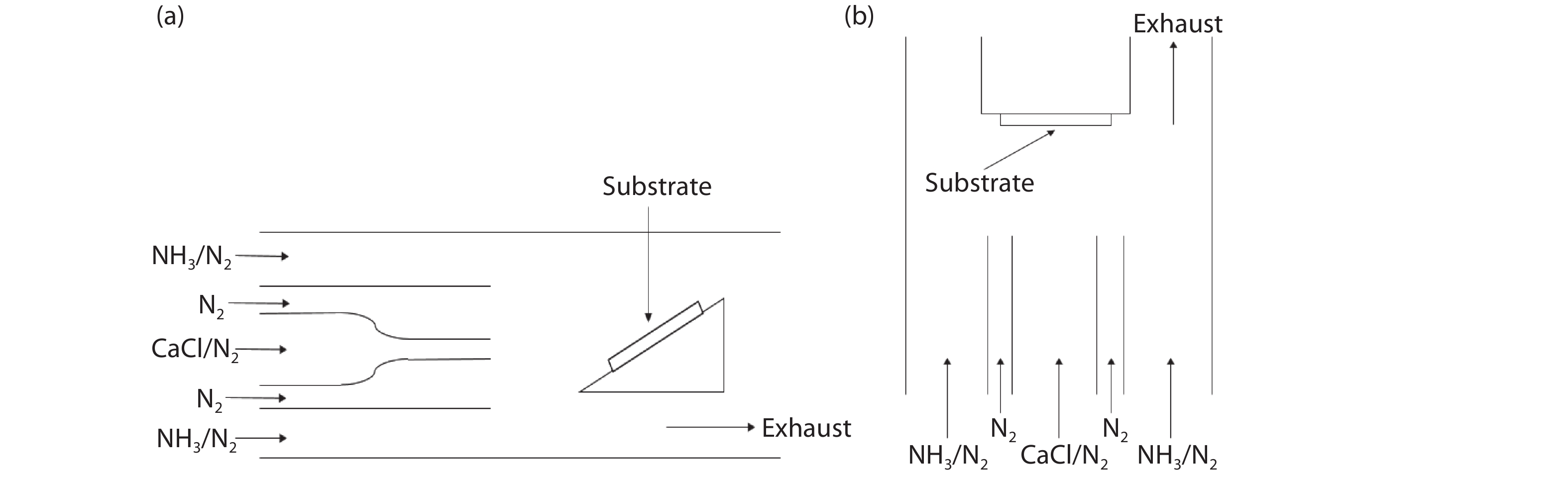
    Fig. 1. Schematic view of (a) horizontal HVPE reactor and (b) vertical HVPE reactor.
    Reactor geometry of Aixtron AIX-HVPE horizontal quartz reactors.
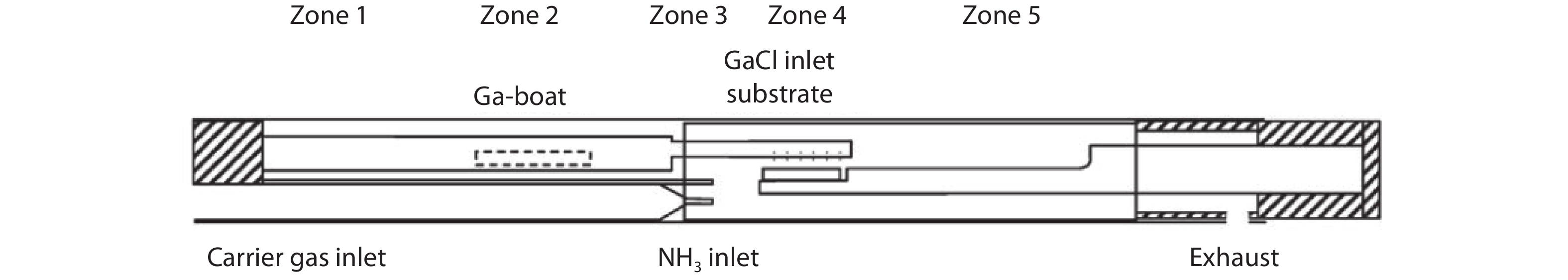
    Fig. 2. Reactor geometry of Aixtron AIX-HVPE horizontal quartz reactors.
    (Color online) AIXTRON vertical HVPE system. (a) Concentric inlet geometry. (b) Schematic sketch of its reactor components.
    Fig. 3. (Color online) AIXTRON vertical HVPE system. (a) Concentric inlet geometry. (b) Schematic sketch of its reactor components.
    (Color online) Photograph of a 6.3 mm thick GaN boule grown by Aixtron vertical HVPE.
    Fig. 4. (Color online) Photograph of a 6.3 mm thick GaN boule grown by Aixtron vertical HVPE.
    (Color online) The appearance of (a) the Kyma100TM HVPE System, (b) K200TM HVPE Growth Tool.
    Fig. 5. (Color online) The appearance of (a) the Kyma100TM HVPE System, (b) K200TM HVPE Growth Tool.
    (Color online) (a) Photograph of fin-shaped porous TaC ceramic component to the Ga evaporator. (b) Schematic drawing of the modified HF-VPE. (c) Photograph of evaporator wetted with molten Ga.
    Fig. 6. (Color online) (a) Photograph of fin-shaped porous TaC ceramic component to the Ga evaporator. (b) Schematic drawing of the modified HF-VPE. (c) Photograph of evaporator wetted with molten Ga.
    (Color online) (a) Scheme of the evaporation cell. The arrows stand for three flows in the reactor: A: transport flow for Ga vapor, B: separation flow, C: NH3 with a carrier gas. (b) Numerical simulation of HTVPE reactor temperature distribution.
    Fig. 7. (Color online) (a) Scheme of the evaporation cell. The arrows stand for three flows in the reactor: A: transport flow for Ga vapor, B: separation flow, C: NH3 with a carrier gas. (b) Numerical simulation of HTVPE reactor temperature distribution.
    (Color online) Schematic illustration of (a) nozzle structure in ID-HVPE and (b) ID-PMG method.
    Fig. 8. (Color online) Schematic illustration of (a) nozzle structure in ID-HVPE and (b) ID-PMG method.
    (Color online) Schematic of (a) simulated mole fraction of precursor in ID-HVPE and (b) thickness distribution of GaN substrate along the diameter.
    Fig. 9. (Color online) Schematic of (a) simulated mole fraction of precursor in ID-HVPE and (b) thickness distribution of GaN substrate along the diameter.
    (Color online) Schematic of (a) new designed nozzle structure in PD-HVPE and (b) simulated mass fraction of precursor in ID-HVPE system and PD-HVPE system on various gas flow rate.
    Fig. 10. (Color online) Schematic of (a) new designed nozzle structure in PD-HVPE and (b) simulated mass fraction of precursor in ID-HVPE system and PD-HVPE system on various gas flow rate.
    (Color online) 3D simulation model of five-susceptor, 6 × 4 inch HVPE reactor.
    Fig. 11. (Color online) 3D simulation model of five-susceptor, 6 × 4 inch HVPE reactor.
    (Color online) Schematic diagram of the HVPE (a) from the vertical cross section view, (b) from the top view.
    Fig. 12. (Color online) Schematic diagram of the HVPE (a) from the vertical cross section view, (b) from the top view.
    (Color online) Schematic diagram of the HVPE reactor and magnified detail of growth/etch zone.
    Fig. 13. (Color online) Schematic diagram of the HVPE reactor and magnified detail of growth/etch zone.
    (Color online) Photograph of a freestanding GaN substrate by in situ removal Si substrate.
    Fig. 14. (Color online) Photograph of a freestanding GaN substrate by in situ removal Si substrate.
    Jun Hu, Hongyuan Wei, Shaoyan Yang, Chengming Li, Huijie Li, Xianglin Liu, Lianshan Wang, Zhanguo Wang. Hydride vapor phase epitaxy for gallium nitride substrate[J]. Journal of Semiconductors, 2019, 40(10): 101801
    Download Citation