
Jun Hu, Hongyuan Wei, Shaoyan Yang, Chengming Li, Huijie Li, Xianglin Liu, Lianshan Wang, Zhanguo Wang. Hydride vapor phase epitaxy for gallium nitride substrate[J]. Journal of Semiconductors, 2019, 40(10): 101801
- Journal of Semiconductors
- Vol. 40, Issue 10, 101801 (2019)
Abstract
1. Introduction
Gallium nitride (GaN) has many noticeable characteristics, such as a wide band gap of 3.4 eV, a high electric breakdown field of 3.3 × 10⁶ V/cm, and a high electron saturation velocity of 2.7 × 107 cm/s, which have led it to be widely applied in optoelectronic devices and power electronic devices. The great success of GaN LEDs is based on their heteroepitaxy structures, even though they have many defects and dislocations due to lattice mismatches. To improve the performance of optoelectronic and power electronic devices, the homoepitaxy GaN device is a promising way of using GaN substrates.
GaN bulk crystals are difficult to obtain by conventional melt solidification crystal growth processes[
Commercial 2 inch GaN substrates produced by HVPE with a thread dislocation density (TDD) in the order of 106 cm–3 are already available from many corporations, and 4 inch or larger scale GaN substrates are also available on the market. In addition, via homebulit HVPE, the lowest TDD 3 × 102 cm–2, of 5 mm-thick 2 inch GaN has been obtained by pit-assisted growth[
HVPE equipment is a key factor to obtain a high-quality GaN substrate. Consequently, equipment vendors have launched commercial equipment to produce GaN substrates of various sizes. Meanwhile, prototype HVPE equipment for higher quality GaN substrates are also in development. In our paper, we review the commercial and prototype HVPE systems for GaN substrates. Finally, we will share our thoughts about the development about HVPE equipment in the future.
2. The principle of HVPE
HVPE is a chemical vapor deposition technology that uses hydride (AsH3, PH3, NH3) and chloride (GaCl, GaCl3, InCl) as source materials for the reaction. According to the function, the HVPE reactor chamber can be divided into two zones: a low-temperature feedstock zone and a high-temperature growth zone, where chemical reaction processes can be described as follows:
High-purity HCl gas reacts with liquid Ga in the low-temperature feedstock zone (~ 850 °C) to generate GaCl gas with a small amount of by-product, which is transported by N2 or other carrier gas to the high-temperature growth region (~ 1050 °C) where GaCl and NH3 are mixed and reacted. The reaction product, GaN, is then deposited on the substrate to form GaN film. The chemical reactions are:
Low-temperature feedstock zone:
High-temperature growth zone:
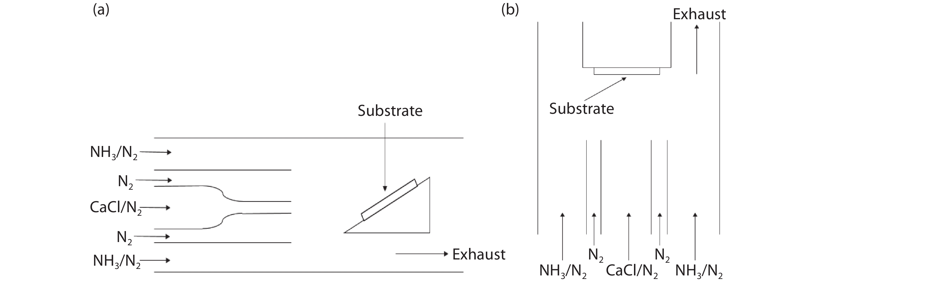
The HVPE reactor system is mainly composed of a gas supply system, a reaction chamber, a heating system, and an exhaust gas system. According to the direction of gas flow in reaction chamber, the HVPE reactor can be divided into two types: vertical HVPE reactors and horizontal HVPE reactors. Fig. 1 shows schematic diagrams of two kinds of typical HVPE reactor.
![]()
Figure 9.(Color online) Schematic of (a) simulated mole fraction of precursor in ID-HVPE and (b) thickness distribution of GaN substrate along the diameter.
3. Commercial HVPE
Since HVPE was first applied in the growth of Ⅲ-nitride semiconductor in the last century[
The earliest commercial HVPE equipment was the Aixtron AIX-HVPE horizontal quartz reactor[
![]()
Figure 10.(Color online) Schematic of (a) new designed nozzle structure in PD-HVPE and (b) simulated mass fraction of precursor in ID-HVPE system and PD-HVPE system on various gas flow rate.
A vertical HVPE system that was developed by AIXTRON was commercialized in 2007s[
![]()
Figure 11.(Color online) 3D simulation model of five-susceptor, 6 × 4 inch HVPE reactor.
Some specific designs have been developed to improve the total growth rate and growth uniformity. The inlet design is concentric and two sheath flows are designed to avoid pre-reaction between two reactive species GaCl and NH3, and to reduce parasitic deposition on the wall and reactor volume. The GaN seed holder can be raised upwards by the boule retraction unit as the GaN film epitaxy grows thicker to keep the distance between the gas inlet and substrate surface constant and optimal. Meanwhile the RF power is completely dissipated in the graphite susceptors, keeping the whole growth zone temperature even and making it a true hot wall reactor. An advanced design is used to lead the exhaust gas out when its temperature is above 350 °C. Ammonium-chloride (NH4Cl), a white powder, is formed in the reactor below 350 °C, which would bring growth defects and result into the blockage of the exhaust gas tube.
With this vertical HVPE, at the growth rate of 250 μm/h, 2 mm thick crack-free GaN films are produced with the etch pit density (EPD), while the layer can reach as low as 5 × 105 cm–2[
Using the same reactor, GaN boules with thicknesses of 2.6, 5.8 and 6.3 mm were successful grown by Ritcher et al.[
![]()
Figure 12.(Color online) Schematic diagram of the HVPE (a) from the vertical cross section view, (b) from the top view.
Kyma Technologies, Inc. have launched HVPE equipment, named Kyma100TM HVPE System[
![]()
Figure 13.(Color online) Schematic diagram of the HVPE reactor and magnified detail of growth/etch zone.
In addition to the Kyma100TM HVPE System, Kyma has also developed another HVPE equipment, which is named K200TM HVPE Growth Tool[
There are other vendors can provide the HVPE systems, such as Oxford Instruments, TGO TECH CO.LTD, TRINITRI-Technology LLC and so on.
4. Developing prototype HVPE
4.1. Halogen-free VPE
For general HVPE system, due to the existence of NH3 and GaCl, the long-duration growth of GaN crystal is limited by the accumulation of NH4Cl.
Halogen-free vapor phase epitaxy (HF-VPE) is a similar technique to general HVPE, whose Ga precursor is Ga vapor and is directly vaporized from melted Ga instead of GaCl gas. The reaction in this process is:
The absence of chlorine makes HF-VPE a reasonable approach to avoid NH4Cl ash in the exhaust gas tube in the downstream of the reactor chamber. This technique is able to meet the requirements for prolonging the time of stable growth of GaN crystal.
Although HF-VPE has some limitations, such as low grow rate and high Ga source temperature, in the 2000s several groups tried to use the HF-VPE process to grow GaN[
Subsequently, Nakamura et al.[
Lukin et al.[
Compared with the HF-VPE mentioned above, the distance between Ga source and substrate is increased, which reduces the thermal coupling in the two temperature zones and alleviates the problem of thermal field interference. This further results in two temperature zones that can be independently controlled by an induction heating module, which increases the flexibility of temperature control. The simulated temperature distribution for typical growth process is shown in Fig. 7(b), where the gallium temperature is 1340 °C, substrate temperature is 1100 °C. The modeling and simulation are performed by COMSOL Multiphysics software, and the fused silica was simplified as a transparent component in radiation, which is the major heat transport mechanism in the target studied system.
Additionally, a Ga evaporator is covered with a molybdenum cap or pyrolytic boron nitride to reduce the introduction of C impurities. A 15 × 15 mm2 substrate was grown with a growth rate of 165 μm/h, demonstrating the potential of growing thick-film GaN by this modified HF-VPE.
4.2. Tri-halide vapor phase epitaxy (THVPE)
THVPE is an interesting alternative to the conventional HVPE, it uses gallium tri-chloride (GaCl3) as the Ⅲ-precursor, instead of using gallium mono-chloride (GaCl) as the Ⅲ-precursor in conventional HVPE, the precursor GaCl3 can be supplied into the growth zone by two approaches, the first approach is directly evaporation or sublimation from the GaCl3[
The source zone:
The growth zone:
For conventional HVPE, its growth rate is currently up to 1870 μm/h[
Besides thermodynamic analysis on THVPE, many experiment related with GaN epitaxy by THVPE has been completed in recent years[
The experiments conducted by Hisashi Murakami et al.[
From the progress shown above, THVPE has showed a potential for epitaxy low-cost, high-crystalline-quality GaN substrates, which is hopeful to replace conventional manufacturing method of GaCl-based HVPE in the future.
In the other hand, the growth temperature of GaN growth with GaCl3 generally exceeds 1100 °C, up to 1350 °C. Therefore, more stringent requirements are imposed on the heating and thermal insulation system of the equipment. What’s worse, differ from conventional HVPE, in which both HCl and N2 exhaust gas are easily soluble in water, so the exhaust gas treatment is relatively easy, Cl2 gas in THVPE is water-insoluble, so additional treatment method are required to treat Cl2. Accordingly, Tri-halide VPE needs more improvements to meet the industrial growth of GaN substrates.
4.3. Large-scale or multi-wafer HVPE
Large-scale or multi-wafer HVPE is an effective way to mass production of GaN substrate. However, the large size of the reactor chamber requires complex design and narrow operating window to keep the uniform growth of GaN substrates.
Zhang et al.[
First, they added an inner dilution gas (ID) pipe (the section is shown in Fig. 8(a)) between Ⅴ and Ⅲ group concentric gas-flow channel to adjust the GaN film thickness distribution, with a specially designed modified gas intake setup, which they called ID gas periodically modulated growth (ID-PMG) method. In other words, the ID gas flow rate changed periodically to adjust the precursor concentration distribution at the substrate surface, the schematic illustration is shown in Fig. 8(b).
The modulation effect of ID-PMG method in ID-HVPE are analyzed by numerical simulation, the simulated precursor concentration distribution above wafers surface is shown in Fig. (9a). Eventually, they have successfully made a HVPE reactor that is able to grow three high-uniformity (±3%–4%) 2 inch substrates at a time, which is a huge improvement compared to that of ± 30% grown by the conventional multi-wafer HVPE. The thickness distribution of GaN layer is shown in Fig. 9(b). Besides, the crystal quality and surface morphology were also improved because the ID gas has suppressed the parasitic reaction.
When applying this modification into single 4 inch GaN wafer growth, the thickness inhomogeneity was worsened to 14% again. Consequently, further improvements have been developed based on their work. For example, an extra dilution and push gas (PD) pipe (the structure of the modified HVPE gas nozzle is shown in Fig. 10(a)) has been added in the center of gas channels in the HVPE system to redistribute the distribution of GaCl and NH3 upon the wafer. The effect of new design on precursor concentration distribution on wafer surface has been simulated, as shown in Fig. 10(b). Consequently, by the optimal gas-flow rate, a single 4 inch GaN substrate with outstanding thickness uniformity has been obtained and the experimental results show that the thickness inhomogeneity of 4-inch GaN substrates can be reduced to ±1.8% compared to the ±14% grown with conventional nozzle. This excellent result shows that this technique offers an effective way to research and develop a HVPE reactor to grow large-size uniform GaN substrates.
According to the report on the website, recently a 2 × 12 inch HVPE equipment has been introduced by Sino Nitride Semiconductor Co, which has successfully grown 15–25 μm GaN/Al2O3 composite substrates using a multi-wafer HVPE. The thickness uniformity of each wafer was about 10%, and the average thickness variation among 21 wafers was less than 5% in the same run.
Yi et al.[
4.4. In situ removal of foreign substrate
At present, the most common process for making a freestanding GaN substrate is to use a laser to lift off the GaN thick film from foreign substrate after the HVPE growth GaN process. When the GaN thick film cools with a foreign substrate, the wafer is prone to bending and cracking due to the lattice mismatches and thermal mismatches. To solve this problem, various buffer layers or weak bonding layers have been introduced to achieve self-separation of the GaN substrates[
Recently, the in situ removal technology of GaN substrates has been realized by Moon Sang Lee et al.[
Lee et al.[
Additionally, according to the researcher, this modified HVPE is a very promising candidate for the production of freestanding 8-inch GaN substrates.
GT Advanced Technologies has also developed HVPE with an in situ laser to lift off the foreign substrate, as published in a presentation made by Raghavan at the LED Forum 2013 in Taipei, China.
5. Conclusion and perspectives
Recently, the increasing demand for high-quality and low-cost GaN substrates has led to various attempts and modifications to be made to develop the HVPE system and corresponding epitaxial GaN processes. Nowadays, GaN substrates can be up to 6 inches in diameter, or even bigger[
This paper describes the principles of HVPE and their different structural designs. It then summarizes the commercial HVPE reactors, and their modifications and innovations. It finally discusses the GaN substrate grown by these reactors.
Even though the GaN substrate grown by HPVE has shown great potential. There are many obstacles needed to be cleared:
First, when the substrates diameter expands from 2 inch to 4 inch or larger, the separation of substrate from foreign substrates become increasing hard, most of them would crack, even if few of them successfully separated from foreign substrates, the wafer would fall into strongly bowed and highly stressed state, which is an issue hard to solve, resulting in the large size GaN substrate unacceptable expensive.
Second, Ammonia chloride (NH4Cl) ash would form in the reactor downstream when the temperature down to 350 °C, the NH4Cl powder bring the blockage problem, which cannot avoid since the existence of NH3 and HCl in reactor chamber. The NH4Cl problem is one of the main factors that hinder the long-duration growth of GaN boule.
The last obstacle is parasitic deposition. the parasitic deposition in the reactor chamber would cost part of precursor, reduce growth rate and yield, what’s worse, the by-product GaN particles which fall down to the wafer surface, bring many defects, such as threading dislocation caused by a combination of parasitic deposition and anisotropy of the growth.
Although so many challenges to solve, the rapidly development on HVPE growth of GaN in recent years are inspiring. We have enough reason to believe that in the near future, high-quality, low-cost large-size freestanding GaN substrates will be realized by a modified HVPE reactor, which is able to grow GaN boule for a long duration or grow multi-GaN wafers in a batch. This would impressively increase the performance of homoepitaxy GaN-based devices and enable them to applied more widely and play a significant role in energy-saving.
Acknowledgments
This work was supported by the National Key Research and Development Plan (No. 2017YFB0404201) and the National Science Foundation of China (Nos. 61774147, 61874108).
References
[1] J A Van Vechten. Quantum dielectric theory of electronegativity in covalent systems. III. pressure-temperature phase diagrams, heats of mixing, and distribution coefficients. Phys Rev B, 7, 1479(1973).
[2] J Karpiński, J Jun, S Porowski. Equilibrium pressure of N2 over GaN and high pressure solution growth of GaN. J Cryst Growth, 66, 1(1984).
[3] M Leszcynski, I Grzegory, M Bockowski. X-ray examination of GaN single crystals grown at high hydrostatic pressure. J Cryst Growth, 126, 601(1993).
[4] H Yamane, M Shimada, S J Clarke et al. Preparation of GaN single crystals using a Na flux. Chem Mater, 9, 413(1997).
[5] K Murakami, D Matsuo, H Imabayashi et al. Effects of solution stirring on the growth of bulk GaN single crystals by Na flux method. Jpn J Appl Phys, 52, 08JA03(2013).
[6] R Dwiliński, R Doradziński, J Garczyński et al. Excellent crystallinity of truly bulk ammonothermal GaN. J Cryst Growth, 310, 3911(2008).
[7] D Ehrentraut, R T Pakalapati, D S Kamber et al. High quality, low cost ammonothermal bulk gan substrates. Jpn J Appl Phys, 52, 08JA01(2013).
[8] M K Kelly, R P Vaudo, V M Phanse et al. Large free-standing GaN substrates by hydride vapor phase epitaxy and laser-induced liftoff. Jpn J Appl Phys, 38, L217(1999).
[9] K Motoki, T Okahisa, N Matsumoto et al. Preparation of large freestanding GaN substrates by hydride vapor phase epitaxy using GaAs as a starting substrate. Jpn J Appl Phys, 40, L140(2001).
[10] Y Oshima, T Eri, M Shibata et al. Preparation of freestanding GaN wafers by hydride vapor phase epitaxy with void-assisted separation. Jpn J Appl Phys, 42, L1(2003).
[11] M Lee, D Mikulik, M Yang et al. Nearly perfect GaN crystal via pit-assisted growth by HVPE. CrystEngComm, 19, 2036(2017).
[12] T Yoshida, M Imanishi, T Kitamura et al. Development of GaN substrate with a large diameter and small orientation deviation. Phys Status Solidi B, 254, 1600671(2017).
[13] H P Maruska, J J Tietjen. The preparation and properties of vapor-deposited single-crystal-line GaN. Appl Phys Lett, 15, 327(1969).
[14] D K Wickenden, K R Faulkner, R W Brander et al. Growth of epitaxial layers of gallium nitride on silicon carbide and corundum substrates. J Cryst Growth, 9, 158(1971).
[15] W Seifert, G Fitzl, E Butter. Study on the growth rate in VPE of GaN. J Cryst Growth, 52, 257(1981).
[16] O Parillaud, V Wagner, H J Buehlmann et al. Localized epitaxy of GaN by HVPE on patterned substrates. MRS Int J Nitride Semicond Res, 3, e40(1998).
[17] E Richter, S Gramlich, A Klein et al. Direct growth of GaN on (0001) sapphire by low pressure hydride vapour phase epitaxy. Phys Status Solidi A, 188, 439(2001).
[18] C Hennig, E Richter, M Weyers et al. Self-separation of thick two inch GaN layers grown by HVPE on sapphire using epitaxial lateral overgrowth with masks containing tungsten. Phys Status Solidi C, 4, 2638(2007).
[19] C Wang, C H Anthony, M Seyboth et al. Influence of growth parameters on crack density in thick epitaxially lateral overgrown GaN layers by hydride vapor phase epitaxy. J Cryst Growth, 230, 377(2001).
[20] C Hemmingsson, P P Paskov, G Pozina et al. Growth of bulk GaN in a vertical hydride vapour phase epitaxy reactor. Superlattices Microstruct, 40, 205(2006).
[21] E Richter, C Hennig, M Weyers et al. Reactor and growth process optimization for growth of thick GaN layers on sapphire substrates by HVPE. J Cryst Growth, 277, 6(2005).
[22]
[23]
[24] C Hemmingsson, P P Paskov, G Pozina et al. Hydride vapour phase epitaxy growth and characterization of thick GaN using a vertical HVPE reactor. J Cryst Growth, 300, 32(2007).
[25] E Richter, U Zeimer, S Hagedorn et al. Hydride vapor phase epitaxy of GaN boules using high growth rates. J Cryst Growth, 312, 2537(2010).
[26] E Richter, M Gründer, B Schineller et al. GaN boules grown by high rate HVPE. Phys Status Solidi C, 8, 1450(2011).
[27] E Richter, M Gründer, C Netzel et al. Growth of GaN boules via vertical HVPE. J Cryst Growth, 350, 89(2012).
[28]
[29]
[30] H Shin, D B Thomson, R Schlesser et al. High temperature nucleation and growth of GaN crystals from the vapor phase. J Cryst Growth, 241, 404(2002).
[31] T Bohnen, H Ashraf, Dreumel G W G van et al. Enhanced growth rates and reduced parasitic deposition by the substitution of Cl2 for HCl in GaN HVPE. J Cryst Growth, 2542(2010).
[32] D Nakamura, T Kimura, K Horibuchi. Halogen-free vapor phase epitaxy for high-rate growth of GaN bulk crystals. Appl Phys Express, 10, 045504(2017).
[33] D Nakamura, T Kimura. Significant increase in GaN growth rate by halogen-free vapor phase epitaxy with porosity-controlled evaporator. Appl Phys Express, 10, 095503(2017).
[34] D Nakamura, T Kimura. Ultrahigh-yield growth of GaN via halogen-free vapor-phase epitaxy. Appl Phys Express, 11, 065502(2018).
[35] T Kimura, K Horibuchi, K Kataoka et al. Macro-defect-free homoepitaxial GaN growth through halogen-free vapor-phase epitaxy on native GaN seeds. J Cryst Growth, 494, 17(2018).
[36] D Nakamura, A Suzumura, K Shigetoh. Sintered tantalum carbide coatings on graphite substrates: Highly reliable protective coatings for bulk and epitaxial growth. Appl Phys Lett, 106, 082108(2015).
[37] D Nakamura. Simple and quick enhancement of SiC bulk crystal growth using a newly developed crucible material. Appl Phys Express, 9, 055507(2016).
[38] D Nakamura, K Shigetoh, A Suzumura. Tantalum carbide coating via wet powder process: From slurry design to practical process tests. J Eur Ceram Soc, 37, 1175(2017).
[39] D Nakamura, T Kimura, T Narita et al. TaC-coated graphite prepared via a wet ceramic process: Application to CVD susceptors for epitaxial growth of wide-bandgap semiconductors. J Cryst Growth, 478, 163(2017).
[40] G Lukin, T Schneider, M Barchuk et al. Modified high temperature vapor phase epitaxy for growth of GaN films: Modified HTVPE for growth of GaN films. Phys Status Solidi A, 214, 1600753(2017).
[41] T Schneider, G Lukin, F Zimmermann et al. Studies on high temperature vapor phase epitaxy of GaN. J Cryst Growth, 468, 212(2017).
[42] G Lukin, C Röder, M Barchuk et al. Investigation of GaN layers grown by high temperature vapor phase epitaxy: Investigation of GaN layers grown by high temperature vapor phase epitaxy. Phys Status Solidi C, 11, 491(2014).
[43]
[44] N Takahashi, R Matsumoto, A Koukitu et al. Vapor phase epitaxy of In
[45] M Topf, G Steude, S Fischer et al. 1998 Low-pressure chemical vapor deposition of GaN epitaxial films. J Cryst Growth, 189/190, 330(1998).
[46] E Varadarajan, P Puviarasu, J Kumar et al. On the chloride vapor-phase epitaxy growth of GaN and its characterization. J Cryst Growth, 260, 43(2004).
[47] H Murakami, N Takekawa, A Shiono et al. Tri-halide vapor phase epitaxy of thick GaN using gaseous GaCl3 precursor. J Cryst Growth, 456, 140(2016).
[48] Y Kumagai, K Takemoto, T Hasegawa et al. Thermodynamics on tri-halide vapor-phase epitaxy of GaN and In
[49] T Yamane, K Hanaoka, H Murakami et al. Tri-halide vapor phase epitaxy of GaN using GaCl3 gas as a group III precursor Phys. Status Solidi C, 8, 1471(2011).
[50] K Iso, N Takekawa, K Matsuda et al. Tri-halide vapor-phase epitaxy of GaN using GaCl3 on polar, semipolar, and nonpolar substrates. Appl Phys Express, 9, 105501(2016).
[51] T Yoshida, Y Oshima, K Watanabe et al. Ultrahigh-speed growth of GaN by hydride vapor phase epitaxy. Phys Status Solidi C, 8, 2110(2011).
[52]
[53] N Takekawa, N Hayashida, D Ohzeki et al. Growth temperatures and the excess chlorine effect of N-polar GaN growth via tri-halide vapor phase epitaxy. J Cryst Growth, 502, 7(2018).
[54] K Iso, K Matsuda, N Takekawa et al. Quasiequilibrium crystal shape and kinetic Wulff plot for GaN grown by trihalide vapor phase epitaxy using GaCl3. Phys Status Solidi B, 254, 1600679(2017).
[55] K Iso, K Matsuda, N Takekawa et al. Thick nonpolar m-plane and semipolar (10(1)over-bar(1)over-bar) GaN on an ammonothermal seed by tri-halide vapor-phase epitaxy using GaCl3. J Cryst Growth, 461, 25(2017).
[56] N Liu, J Wu, W Li et al. Highly uniform growth of 2-inch GaN wafers with a multi-wafer HVPE system. J Cryst Growth, 388, 132(2014).
[57] Y Cheng, P Liu, J Wu et al. High uniform growth of 4-inch GaN wafer via flow field optimization by HVPE. J Cryst Growth, 445, 24(2016).
[58] X F Han, M J Hur, J H Lee et al. Numerical simulation of the gallium nitride thin film layer grown on 6-inch wafer by commercial multi-wafer hydride vapor phase epitaxy. J Cryst Growth, 406, 53(2014).
[59] X F Han, J H Lee, Y J Lee et al. Numerical analysis on the origin of thickness unevenness and formation of pits at GaN thin film grown by HVPE. J Cryst Growth, 450, 66(2016).
[60] X F Han, J H Lee, Y J Lee et al. 3D numerical analysis of influence of the non-uniform deposition rate on the hillock density at HVPE-GaN surface. J Cryst Growth, 474, 81(2017).
[61] W Luo, J Wu, J Goldsmith et al. The growth of high-quality and self-separation GaN thick-films by hydride vapor phase epitaxy. J Cryst Growth, 340, 18(2012).
[62] M Amilusik, T Sochacki, B Łucznik et al. Analysis of self-lift-off process during HVPE growth of GaN on MOCVD-GaN/sapphire substrates with photolitographically patterned Ti mask. J Cryst Growth, 380, 99(2013).
[63] Y Sui, B Wang, Z Zhao et al. Facet growth of self-separated GaN layers through HVPE on large square-patterned template. J Cryst Growth, 394, 11(2014).
[64] M Lee, D Mikulik, M Yang et al. The investigation of stress in freestanding GaN crystals grown from Si substrates by HVPE. Sci Rep, 7, 8587(2017).
[65] M Lee, D Mikulik, J Kim et al. A novel growth method of freestanding GaN using in situ removal of Si substrate in hydride vapor phase epitaxy. Appl Phys Express, 6, 125502(2013).
[66] M Lee, D Mikulik, S Park. The investigation of in situ removal of Si substrates for freestanding GaN crystals by HVPE. RSC Adv, 8, 12310(2018).


Set citation alerts for the article
Please enter your email address

© Copyright 2018-2021 | Chinese Laser Press. All Rights Reserved 沪ICP备15018463号-20