• Journal of Semiconductors
  • Vol. 41, Issue 8, 082002 (2020)
Chang Li1、2, Cheng Chen2、3, Jie Chen2、3, Tao He4, Hongwei Li2、5, Zeyuan Yang1、2, Liu Xie2, Zhongchang Wang6, and Kai Zhang2
Author Affiliations
  • 1Nano Science and Technology Institute, University of Science and Technology of China, Suzhou 215123, China
  • 2i-Lab, Suzhou Institute of Nano-Tech and Nano-Bionics (SINANO), Chinese Academy of Sciences, Suzhou 215123, China
  • 3School of Materials Science and Engineering, Shanghai University, Shanghai 200444, China
  • 4CAS Key Laboratory of Nanodevices and Applications, Suzhou Institute of Nano-Tech and Nano-Bionics (SINANO), Chinese Academy of Sciences, Suzhou 215123, China
  • 5Institute of Microscale Optoelectronics, Collaborative Innovation Centre for Optoelectronic Science & Technology, Key Laboratory of Optoelectronic Devices and Systems of Ministry of Education and Guangdong Province, College of Physics and Optoelectronic Engineering, Shenzhen Key Laboratory of Micro-Nano Photonic Information Technology, Guangdong Laboratory of Artificial Intelligence and Digital Economy (SZ), Shenzhen University, Shenzhen 518060, China
  • 6International Iberian Nanotechnology Laboratory (INL), Avenida Mestre José Veiga s/n, Braga 4715-330, Portugal
  • show less
    DOI: 10.1088/1674-4926/41/8/082002 Cite this Article
    Chang Li, Cheng Chen, Jie Chen, Tao He, Hongwei Li, Zeyuan Yang, Liu Xie, Zhongchang Wang, Kai Zhang. High-performance junction field-effect transistor based on black phosphorus/β-Ga2O3 heterostructure[J]. Journal of Semiconductors, 2020, 41(8): 082002 Copy Citation Text show less
    (Color online) (a) Optical microscope images of fabrication steps of BP/β-Ga2O3 heterojunction device. The channel length and width of the β-Ga2O3 were 16 and 6 μm, respectively. (b) SEM image of an as-fabricated BP/β-Ga2O3 heterojunction device. (c) Schematic illustration of the JFET device fabricated on a Si/SiO2 (285 nm) substrate. (d) Energy band diagram of multilayer p-type BP and n-type β-Ga2O3 heterojunctions with a vdW gap. Scale bars are 10 µm.
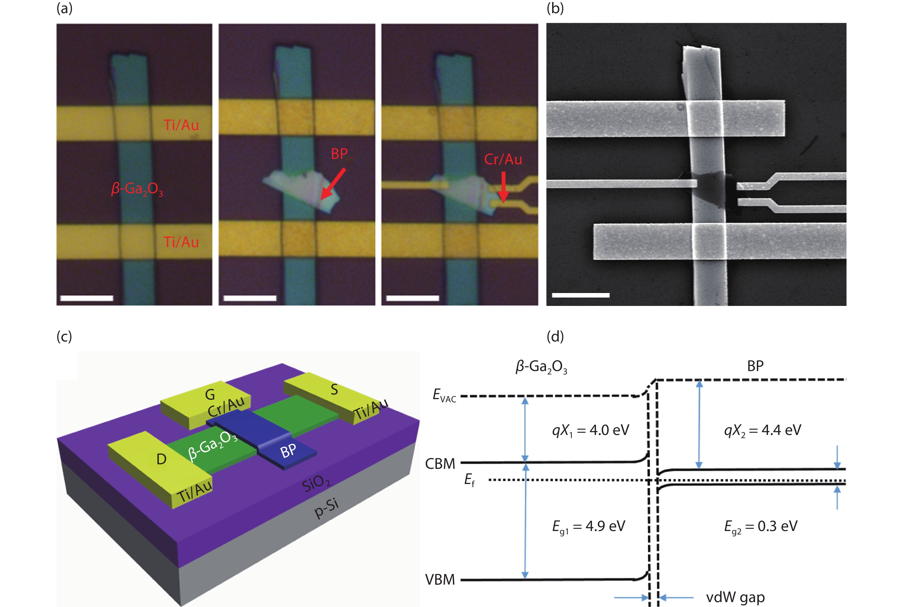
    Fig. 1. (Color online) (a) Optical microscope images of fabrication steps of BP/β-Ga2O3 heterojunction device. The channel length and width of the β-Ga2O3 were 16 and 6 μm, respectively. (b) SEM image of an as-fabricated BP/β-Ga2O3 heterojunction device. (c) Schematic illustration of the JFET device fabricated on a Si/SiO2 (285 nm) substrate. (d) Energy band diagram of multilayer p-type BP and n-type β-Ga2O3 heterojunctions with a vdW gap. Scale bars are 10 µm.
    (Color online) (a) AFM image of the BP/β-Ga2O3 heterojunction. (b, c) Height profiles of the exfoliated BP and β-Ga2O3 flakes in (a). The thicknesses of the nanoflakes are 32.6 and 123.5 nm, respectively. (d) Raman spectra of the BP, β-Ga2O3 and the BP/β-Ga2O3 overlapped regions obtained under a 532 nm laser. The black and green curve demonstrated typical multilayer BP flake and β-Ga2O3 flake. The red curve shows the peaks of the overlapped region. (e) SEM image of the BP/β-Ga2O3 heterostructure device (left) and corresponding EDS element mappings for Ga and P (right). Scale bars are 5 µm.
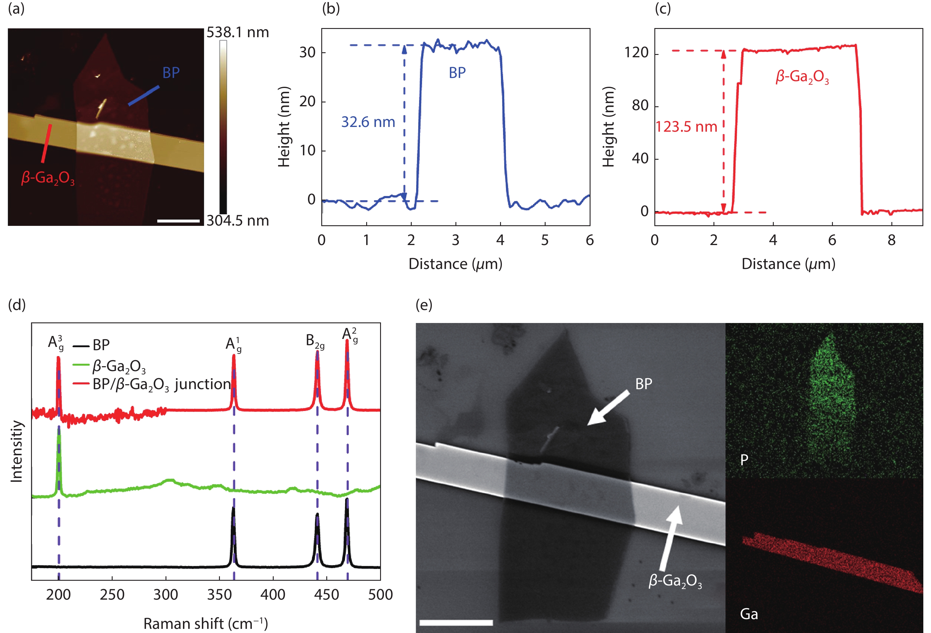
    Fig. 2. (Color online) (a) AFM image of the BP/β-Ga2O3 heterojunction. (b, c) Height profiles of the exfoliated BP and β-Ga2O3 flakes in (a). The thicknesses of the nanoflakes are 32.6 and 123.5 nm, respectively. (d) Raman spectra of the BP, β-Ga2O3 and the BP/β-Ga2O3 overlapped regions obtained under a 532 nm laser. The black and green curve demonstrated typical multilayer BP flake and β-Ga2O3 flake. The red curve shows the peaks of the overlapped region. (e) SEM image of the BP/β-Ga2O3 heterostructure device (left) and corresponding EDS element mappings for Ga and P (right). Scale bars are 5 µm.
    (Color online) (a)Transfer characteristics for back-gate BP FET. Back gate voltage Vbg swept from –60 to 60 V with a fixed source–drain bias voltage Vds = 0.1 V. (Inset: output characteristics for back gated BP FET. Vbg ranging from –60 to 60 V with steps of 30 V under Vds swept from 0 to 50 mV.) (b) Transfer characteristics for back gate β-Ga2O3 FET. Vbg swept from –80 to 80 V with a fixed Vds = 5 V (Inset: output characteristics for back-gate β-Ga2O3 FET. Vbg ranging from –80 to 80 V with steps of 40 V under Vds swept from 0 to 5 V.) (c) Ids−Vds curve of BP/β-Ga2O3 PN heterojunction. It shows a typical rectifying behavior. (Inset: the circuit schematic diagram of the PN heterojunction.) (d) Ids−Vds semi-log plot of the BP/β-Ga2O3 PN heterojunction.
    Fig. 3. (Color online) (a)Transfer characteristics for back-gate BP FET. Back gate voltage Vbg swept from –60 to 60 V with a fixed source–drain bias voltage Vds = 0.1 V. (Inset: output characteristics for back gated BP FET. Vbg ranging from –60 to 60 V with steps of 30 V under Vds swept from 0 to 50 mV.) (b) Transfer characteristics for back gate β-Ga2O3 FET. Vbg swept from –80 to 80 V with a fixed Vds = 5 V (Inset: output characteristics for back-gate β-Ga2O3 FET. Vbg ranging from –80 to 80 V with steps of 40 V under Vds swept from 0 to 5 V.) (c) IdsVds curve of BP/β-Ga2O3 PN heterojunction. It shows a typical rectifying behavior. (Inset: the circuit schematic diagram of the PN heterojunction.) (d) IdsVds semi-log plot of the BP/β-Ga2O3 PN heterojunction.
    (Color online) (a) Circuit schematic diagram and optical image of the BP/β-Ga2O3 JFET. (b) Band diagram of β-Ga2O3 along the channel length direction. The red and blue curve shows the band bending at zero and negative gate voltage, respectively. (c) Output characteristics (Ids−Vds) of the JFET. Vgs ranging from –15 to 2 V under Vds swept from 0 to 25 V. (d) Transfer characteristics (Ids−Vgs) of the JFET. Vds ranging from 2 to 20 V under Vgs swept from –25 to 2 V. (e) Semi-log plot of the transfer characteristics of the JFET. It shows a high on/off ratio beyond 107. (f) Transconductance curves (estimated from transfer curves of (d)) of BP/β-Ga2O3 JFET as function of Vgs with Vds sweeping from 2 to 20 V.
    Fig. 4. (Color online) (a) Circuit schematic diagram and optical image of the BP/β-Ga2O3 JFET. (b) Band diagram of β-Ga2O3 along the channel length direction. The red and blue curve shows the band bending at zero and negative gate voltage, respectively. (c) Output characteristics (IdsVds) of the JFET. Vgs ranging from –15 to 2 V under Vds swept from 0 to 25 V. (d) Transfer characteristics (IdsVgs) of the JFET. Vds ranging from 2 to 20 V under Vgs swept from –25 to 2 V. (e) Semi-log plot of the transfer characteristics of the JFET. It shows a high on/off ratio beyond 107. (f) Transconductance curves (estimated from transfer curves of (d)) of BP/β-Ga2O3 JFET as function of Vgs with Vds sweeping from 2 to 20 V.
    (Color online) (a) Output characteristics curves of the BP/β-Ga2O3 JFET under different temperatures (ranging from 300 to 450 K with steps of 50 K) at Vgs = 1 V. (b) Transfer characteristics curves of the BP/β-Ga2O3 JFET under different temperatures (ranging from 300 to 450 K with steps of 50 K) at Vds = 10 V.
    Fig. 5. (Color online) (a) Output characteristics curves of the BP/β-Ga2O3 JFET under different temperatures (ranging from 300 to 450 K with steps of 50 K) at Vgs = 1 V. (b) Transfer characteristics curves of the BP/β-Ga2O3 JFET under different temperatures (ranging from 300 to 450 K with steps of 50 K) at Vds = 10 V.
    Chang Li, Cheng Chen, Jie Chen, Tao He, Hongwei Li, Zeyuan Yang, Liu Xie, Zhongchang Wang, Kai Zhang. High-performance junction field-effect transistor based on black phosphorus/β-Ga2O3 heterostructure[J]. Journal of Semiconductors, 2020, 41(8): 082002
    Download Citation