
Chang Li, Cheng Chen, Jie Chen, Tao He, Hongwei Li, Zeyuan Yang, Liu Xie, Zhongchang Wang, Kai Zhang. High-performance junction field-effect transistor based on black phosphorus/β-Ga2O3 heterostructure[J]. Journal of Semiconductors, 2020, 41(8): 082002
- Journal of Semiconductors
- Vol. 41, Issue 8, 082002 (2020)
Abstract
1. Introduction
As an emerging material with an ultra-wide bandgap (4.9 eV) at room temperature, high theoretical critical field strength (8 MV/cm), superior power switching capability and large Baliga’s figure of merit, β-gallium oxide (β-Ga2O3) has been considered a competitive material for the next generation of high power electronic and optoelectronic devices. The unintentionally doped β-Ga2O3 exhibits inherent n-type conductivity because the oxygen vacancy acts as a donor[
Recently, Barman et al. proved the single-crystalline β-Ga2O3 can be exfoliated into nanoflakes along the (100) plane direction while maintaining the superior properties of bulk crystals, even though it's not a layered 2D material bound together through the van der Waals (vdW) force[
As a novel 2D layered semiconductor material, black phosphorous (BP) is gradually receiving considerable attention, because it possesses a tunable direct bandgap (0.3 to 1.5 eV) by thickness (bulk to monolayer), high carrier mobility over 1000 cm2V−1s−1, strong light-matter coupling, excellent intrinsic in-plane anisotropy and exciting biocompatibility[
In this work, we demonstrate a vdW heterojunction JFET based on BP and β-Ga2O3. The mechanically exfoliated multilayer BP flakes as the gate and multilayer β-Ga2O3 flakes as the channel. The BP/β-Ga2O3 PN junction exhibits preeminent rectification characteristics with rectifying ratio higher than 107 and the reverse current as low as pA. The BP/β-Ga2O3 JFETs show excellent n-channel JFET characteristics with high on/off ratio about ~107, low gate leakage current around pA, high gm of 25.3 µS and IDSS of 16.5 µA/µm. Moreover, it has a pinch-off voltage of –20 V and a minimum subthreshold swing of 260 mV/dec. Additionally, the electrical performances of the BP/β-Ga2O3 JFET device at different temperatures are also discussed. This work not only expands the applications of BP in future nanoelectronic devices but also paves the way for vdW heterojunctions based on 2D semiconductors applying to realize high performance JFET devices.
2. Experiments
Material Characterizations: All nanoflakes were measured for thickness information and surface morphology through an atomic force microscope (AFM, Bruker Dimension ICON). Raman measurements were conducted in a micro-Raman system (LABRAM HR) with visible laser light (λ = 532 nm). The morphology and elemental mapping of the heterojunction were observed by scanning electron microscope (SEM, Quanta FEG 250).
Device Fabrication: Using traditional dry transfer technology, the BP/β-Ga2O3 heterojunction was fabricated inside a glove box. First, β-Ga2O3 flakes were prepared from a bulk single-crystalline (100) β-Ga2O3 through the conventional mechanical exfoliation method and transferred onto Si/SiO2 (285 nm) substrates. In order to remove the organic impurity, the substrates with β-Ga2O3 flakes were soaked into acetone for several hours before the device fabrication. Then, the source–drain electrodes of Ti/Au (30/120 nm) were fabricated using electron-beam lithography (JEOL JBX 5500) to define patterns, electron beam evaporator (ULVAC Ei-5Z) to deposit metal films and lift-off process. In order to achieve ohmic contact, rapid thermal annealing was carried out for 60 s at 475 °C in a nitrogen ambient. Afterwards, using the same way, few-layer BP flakes were separated from bulk BP crystals synthesized by mineralizer-assisted gas-phase transformation method. The exfoliated BP flakes were precisely transferred onto β-Ga2O3 through a picking-up and dropping process using the polydimethylsiloxane (PDMS) transfer technique. Finally, the contact metallization with BP was performed by depositing Cr/Au (10/70 nm) using the same method mentioned above. To avoid oxidation from O2 and H2O, the exposure time in ambient was limited within one hour during the fabrication process.
Electrical Characterizations: The electrical characteristics of the fabricated JFET were measured by a Sussmicrotec probe station with a Keithley 4200 semiconductor parameter analyzer.
3. Results and discussion
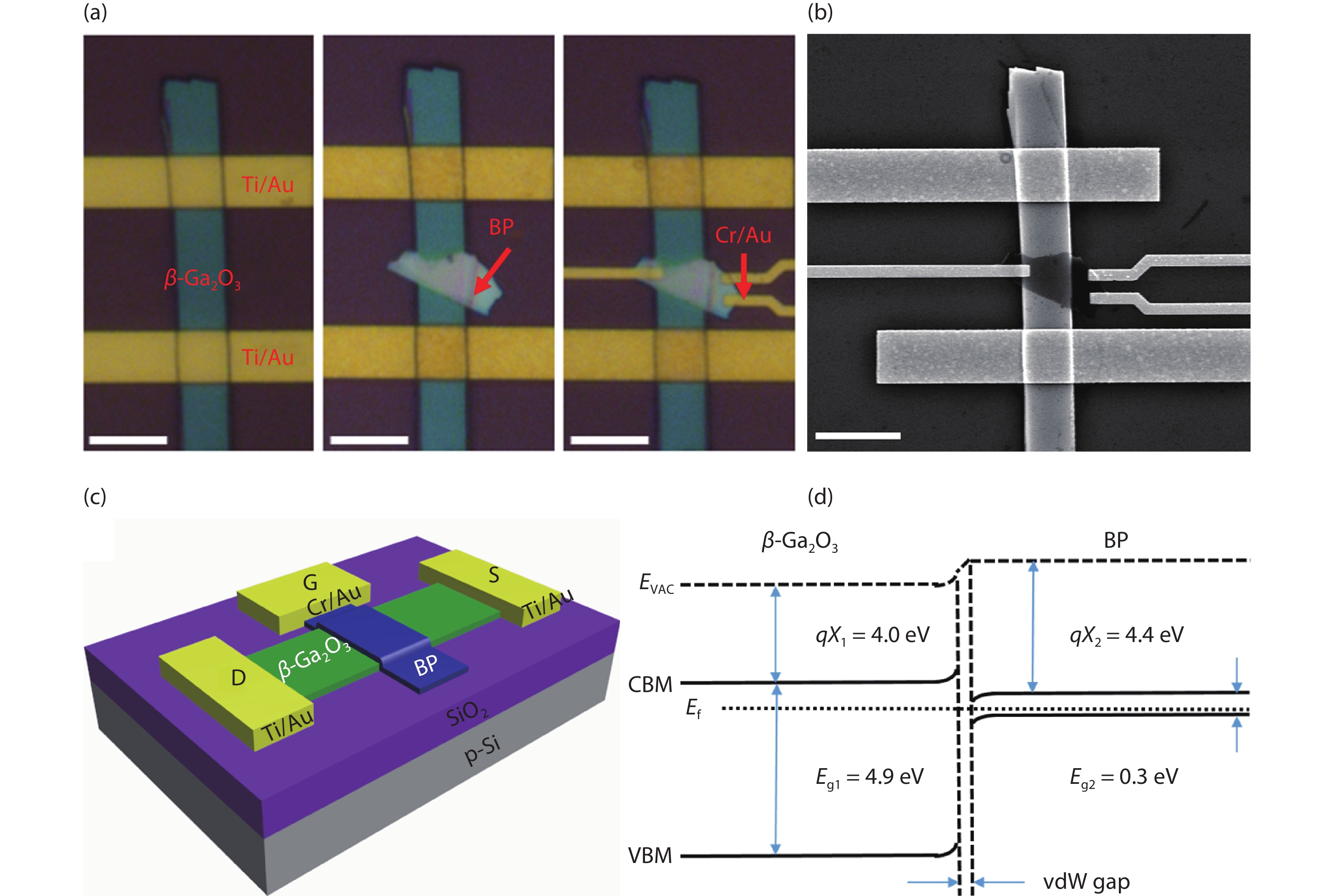
Fig. 1(a) shows the fabrication process of the BP/β-Ga2O3 heterojunction JFET device by using optical microscope images. Multilayer β-Ga2O3 flakes are prepared via mechanically exfoliation. BP/β-Ga2O3 heterojunctions are fabricated by the vdW force using an alignment dry transfer method (for more details, see Experiments). The quality of the as-fabricated BP/β-Ga2O3 heterojunction can be obtained from the SEM image (Fig. 1(b)). The surfaces of both BP and β-Ga2O3 materials were smooth and the heterojunction interface was clean. Fig. 1(c) shows schematic illustration of the BP/β-Ga2O3 heterojunction device on the Si/SiO2 substrate. In this heterojunction device, the source–drain voltages (Vds) is applied on β-Ga2O3, BP and Si/SiO2 act as the gate and back gate, respectively. As shown in Fig. 1(d), the energy band diagram of BP/β-Ga2O3 heterojunction demonstrates the formation of a typical PN junction. According to the previous reports, the electron affinity (qX1) and bandgap (Eg1) values of multilayer β-Ga2O3 are about 4.0 and 4.9 eV, respectively[
![]()
Figure 1.(Color online) (a) Optical microscope images of fabrication steps of BP/
In order to obtain the thickness and surface morphology of the BP/β-Ga2O3 heterojunction, the AFM image and height profiles are presented in Figs. 2(a)−2(c). The thickness of BP is about 32.6 nm with β-Ga2O3 flakes of 123.5 nm. Moreover, AFM image indicates that a vertical heterojunction can be fabricated by directly covering the multilayer BP on the β-Ga2O3 flake. Fig. 2(d) shows the Raman spectrum of BP, β-Ga2O3 and the BP/β-Ga2O3 heterojunction (overlapped region) on the Si/SiO2 substrate. Three characteristic peaks of BP located at 362, 440, and 467 cm−1, corresponding to Ag1, B2g, and Ag2 vibration modes, respectively[
![]()
Figure 2.(Color online) (a) AFM image of the BP/
To demonstrate the fabricated BP/β-Ga2O3 PN heterojunction is available, the electrical properties of the as-fabricated BP/β-Ga2O3 heterojunction FETs as well as the individual BP and β-Ga2O3 devices are exhibited in Fig. 3. Fig. 3(a) shows the source–drain current Ids as a function of back gate voltage (Vbg) at a fixed source–drain bias voltage (Vds = 0.1 V) for the BP FET. Meanwhile, the Ids–Vds curves under different Vbg (ranging from –60 to 60 V with steps of 30 V) are presented in the inset of Fig. 3(a). The device shows a typical p-type ambipolar transistor, which is consistent with previous reports[
![]()
Figure 3.(Color online) (a)Transfer characteristics for back-gate BP FET. Back gate voltage
To further investigate the properties of the BP/β-Ga2O3 PN heterojunction, BP/β-Ga2O3 JFET devices were fabricated. The circuit schematic diagram and optical image of the BP/β-Ga2O3 JFET are shown in the Fig. 4(a). Using the p-type BP as the gate and n-type β-Ga2O3 as the channel, a PN heterojunction formed at the BP/β-Ga2O3 vdW interface. According to the operational mechanism of JFETs, the diode characteristics within the gate-channel PN junction are crucial in determining the final JFET characteristics[
![]()
Figure 4.(Color online) (a) Circuit schematic diagram and optical image of the BP/
where Nd is the unintentional doping carrier density; μ is the field-effect mobility; q is an electronic charge; and L, t, and W are the length, thickness and width of the channel, respectively. So, the field-effect mobility μ can be calculated as follows,
The maximum field-effect mobility μmax of the BP/β-Ga2O3 JFET is 14.7 cm2V−1s−1 when gm is 25.3 µS. The subthreshold swing (SS) is another important parameter for describing the performance of transistors. To achieve lower power consumption and higher integration, it is essential to minimize the SS. The theoretical limit of JFET SS value is 60 mV/dec due to the lack of complicated dielectric engineering. To investigate the performance of BP/β-Ga2O3 JFET in thesubthreshold regime, the minimum SS of 260 mV/dec is reached when Vds = 20 V and Vgs = –21 V. Reducing the thickness and effective carrier concentration of β-Ga2O3 nanosheets will be available for further improving the SS of BP/β-Ga2O3 JFET devices.
To understand the working regimes of the BP/β-Ga2O3 JFET device at different temperatures, temperature-dependent electrical characteristics tests were carried out. The typical output and transfer characteristics at various temperatures (ranging from 300 to 450 K with steps of 50 K) are presented in Figs. 5(a) and 5(b), respectively. Obviously, the JFET characteristics were well maintained. According to the output characteristics curves of the BP/β-Ga2O3 JFET device under various temperatures (Fig. 5(a)), obvious Ids saturation and three stages for typical JFET characteristics (linear, pinch-off and saturation) are observed. While, the Ids decreased with the increasing temperature probably because of lower carrier mobility and enhanced phonon scattering. As shown in Fig. 5(b), transfer characteristics curves of the BP/β-Ga2O3 JFET device under different temperatures demonstrate typical JFET characteristics that Vgs control Ids. The pinch-off voltage is about –18 V, Ids is switched off when Vgs < –18 V and switched on when Vgs > –18 V, corresponding to effectively switched off/on of the JFET.
![]()
Figure 5.(Color online) (a) Output characteristics curves of the BP/
4. Conclusion
Herein, we have successfully fabricated vdW heterojunction JFET devices based on multilayer p-type BP as the gate and n-type β-Ga2O3 flakes as the channel by mechanically exfoliated methods. The BP/β-Ga2O3 heterojunctions possess clean interfaces. Furthermore, the BP/β-Ga2O3 PN junction devices show clear rectification characteristics of a high rectifying ratio about 107 and low reverse current around pA. These strongly rectifying behaviors demonstrate that a good van der Waals PN heterojunction formed between p-type BP and n-type β-Ga2O3. More importantly, the fabricated JFET devices show excellent n-channel JFET properties such as high Ids on/off ratio of 107, low gate leakage current around pA, high gm of 25.3 µS and IDSS of 16.5 µA/µm. In addition, the devices have a pinch-off voltage of –20 V and a minimum subthreshold swing of 260 mV/dec. The temperature-dependent electrical characteristics of JFET devices are also discussed. The JFET characteristics are well maintained although the Ids decreased with the increasing temperature. This work paves the way for vdW heterojunctions based on 2D semiconductors whose application will realize high-performance JFET devices.
Acknowledgements
This work was supported by the National Natural Science Foundation of China (Grant No. 61922082, 61875223, 61927813) and the Natural Science Foundation of Jiangsu Province (Grant No. BK20191195). The support from the Vacuum Interconnected Nanotech Workstation (Nano-X) of Suzhou Institute of Nano-tech and Nano-bionics (SINANO), Chinese Academy of Sciences, is also acknowledged.
References
[1] M Orita, H Ohta, M Hirano et al. Deep-ultraviolet transparent conductive
[2] S J Pearton, J C Yang, P H Cary et al. A review of Ga2O3 materials, processing, and devices. Appl Phys Rev, 5, 011301(2018).
[3] H Zhou, J C Zhang, C F Zhang et al. A review of the most recent progresses of state-of-art gallium oxide power devices. J Semicond, 40, 011803(2019).
[4] H Dong, H W Xue, Q M He et al. Progress of power field effect transistor based on ultra-wide bandgap Ga2O3 semiconductor material. J Semicond, 40, 011802(2019).
[5] M Higashiwaki, K Sasaki, H Murakami et al. Recent progress in Ga2O3power devices. Semicond Sci Technol, 31, 034001(2016).
[6] W S Hwang, A Verma, H Peelaers et al. High-voltage field effect transistors with wide-bandgap
[7] S Ahn, F Ren, J Kim et al. Effect of front and back gates on
[8] J Kim, M A Mastro, M J Tadjer et al. Heterostructure WSe2–Ga2O3 junction field-effect transistor for low-dimensional high-power electronics. ACS Appl Mater Interfaces, 10, 29724(2018).
[9] J Guo, L Y Wang, Y W Yu et al. SnSe/MoS2 van der Waals heterostructure junction field-effect transistors with nearly ideal subthreshold slope. Adv Mater, 31, 1902962(2019).
[10] Z Hajnal, J Miró, G Kiss et al. Role of oxygen vacancy defect states in then-type conduction of
[11] S K Barman, M N Huda. Mechanism behind the easy exfoliation of Ga2O3 ultra-thin film along (100) surface. Phys Status Solidi RRL, 13, 1800554(2019).
[12] Y Liu, Y Huang, X F Duan. Van der Waals integration before and beyond two-dimensional materials. Nature, 567, 323(2019).
[13] X D Yan, I S Esqueda, J H Ma et al. High breakdown electric field in
[14] J Kim, J H Kim. Monolithically integrated enhancement-mode and depletion-mode
[15] J Kim, M A Mastro, M J Tadjer et al. Quasi-two-dimensional h-BN/
[16] L K Li, Y J Yu, G J Ye et al. Black phosphorus field-effect transistors. Nat Nanotechnol, 9, 372(2014).
[17] H Liu, A T Neal, Z Zhu et al. Phosphorene: an unexplored 2D semiconductor with a high hole mobility. ACS Nano, 8, 4033(2014).
[18] F N Xia, H Wang, Y C Jia. Rediscovering black phosphorus as an anisotropic layered material for optoelectronics and electronics. Nat Commun, 5, 4458(2014).
[19] Z Q Zhou, Y Cui, P H Tan et al. Optical and electrical properties of two-dimensional anisotropic materials. J Semicond, 40, 061001(2019).
[20] Y J Xu, Z Shi, X Y Shi et al. Recent progress in black phosphorus and black-phosphorus-analogue materials: Properties, synthesis and applications. Nanoscale, 11, 14491(2019).
[21] J S Qiao, X H Kong, Z X Hu et al. High-mobility transport anisotropy and linear dichroism in few-layer black phosphorus. Nat Commun, 5, 4475(2014).
[22] B C Deng, V Tran, Y J Xie et al. Efficient electrical control of thin-film black phosphorus bandgap. Nat Commun, 8, 14474(2017).
[23] Y J Xu, X Y Shi, Y S Zhang et al. Epitaxial nucleation and lateral growth of high-crystalline black phosphorus films on silicon. Nat Commun, 11, 1330(2020).
[24] N Youngblood, C Chen, S J Koester et al. Waveguide-integrated black phosphorus photodetector with high responsivity and low dark current. Nat Photonics, 9, 247(2015).
[25] X L Chen, X B Lu, B C Deng et al. Widely tunable black phosphorus mid-infrared photodetector. Nat Commun, 8, 1672(2017).
[26] W K Zhu, X Wei, F G Yan et al. Broadband polarized photodetector based on p-BP/n-ReS2 heterojunction. J Semicond, 40, 092001(2019).
[27] M Batmunkh, M Bat-Erdene, J G Shapter. Black phosphorus: Synthesis and application for solar cells. Adv Energy Mater, 8, 1701832(2018).
[28] Y Yang, J Gao, Z Zhang et al. Black phosphorus based photocathodes in wideband bifacial dye-sensitized solar cells. Adv Mater, 28, 8937(2016).
[29] S K Muduli, E Varrla, S A Kulkarni et al. 2D black phosphorous nanosheets as a hole transporting material in perovskite solar cells. J Power Sources, 371, 156(2017).
[30] A G Ricciardulli, P W M Blom. Solution-processable 2D materials applied in light-emitting diodes and solar cells. Adv Mater Technol, 1900972(2020).
[31] X X Ge, Z H Xia, S J Guo. Recent advances on black phosphorus for biomedicine and biosensing. Adv Funct Mater, 29, 1900318(2019).
[32] G Wu, X J Wu, Y J Xu et al. High-performance hierarchical black-phosphorous-based soft electrochemical actuators in bioinspired applications. Adv Mater, 31, 1806492(2019).
[33] W Tao, N Kong, X Y Ji et al. Emerging two-dimensional monoelemental materials (Xenes) for biomedical applications. Chem Soc Rev, 48, 2891(2019).
[34] M Qiu, D Wang, W Y Liang et al. Novel concept of the smart NIR-light-controlled drug release of black phosphorus nanostructure for cancer therapy. Proc Natl Acad Sci USA, 115, 501(2018).
[35] Y J Xu, J Yuan, K Zhang et al. Field-induced n-doping of black phosphorus for CMOS compatible 2D logic electronics with high electron mobility. Adv Funct Mater, 27, 1702211(2017).
[36] W Lv, X Fu, X Luo et al. Multistate logic inverter based on black phosphorus/SnSeS heterostructure. Adv Electron Mater, 5, 1800416(2019).
[37] P J Jeon, Y T Lee, J Y Lim et al. Black phosphorus-zinc oxide nanomaterial heterojunction for p–n diode and junction field-effect transistor. Nano Lett, 16, 1293(2016).
[38] J Y Lim, M Kim, Y Jeong et al. Van der Waals junction field effect transistors with both n- and p-channel transition metal dichalcogenides. npj 2D Mater Appl, 2, 37(2018).
[39] J H Wang, D N Liu, H Huang et al. In-plane black phosphorus/dicobalt phosphide heterostructure for efficient electrocatalysis. Angew Chem Int Ed, 57, 2600(2018).
[40] Y Zheng, Z H Yu, H H Ou et al. Black phosphorus and polymeric carbon nitride heterostructure for photoinduced molecular oxygen activation. Adv Funct Mater, 28, 1705407(2018).
[41] Q Y He, Y Liu, C L Tan et al. Quest for p-type two-dimensional semiconductors. ACS Nano, 13, 12294(2019).
[42] Y X Deng, Z Luo, N J Conrad et al. Black phosphorus-monolayer MoS2 van der Waals heterojunction p–n diode. ACS Nano, 8, 8292(2014).
[43] Q Lv, F G Yan, N Mori et al. Interlayer band-to-band tunneling and negative differential resistance in van der Waals BP/InSe field-effect transistors. Adv Funct Mater, 30, 1910713(2020).

Set citation alerts for the article
Please enter your email address
© Copyright 2018-2021 | Chinese Laser Press. All Rights Reserved 沪ICP备15018463号-20