
Raheela Rasool, Najeeb-ud-Din, G. M. Rather. Analytical model for the effects of the variation of ferrolectric material parameters on the minimum subthreshold swing in negative capacitance capacitor[J]. Journal of Semiconductors, 2019, 40(12): 122401
- Journal of Semiconductors
- Vol. 40, Issue 12, 122401 (2019)
Abstract
1. Introduction
Negative capacitance field effect transistor (NC-FET) was proposed in 2008 by Salahuddin et al.[
In this paper, we have obtained an analytical equation to determine the thickness of the ferroelectric material required to get minimum subthreshold swing, under capacitance matching condition. The limit on minimum possible subthreshold swing (Smin) reflects the choice of underlying MOS capacitance (CMOS) and ferroelectric capacitance (CFE), which is fundamentally dictated by the need to stabilise the total NC capacitor capacitance. In section 2, we describe the fundamental capacitance constraints that define the minimum subthreshold swing in an NC capacitor. In section 3, we determine the optimal thickness of the ferroelectric material and substrate doping required to observe the NC effect for a minimum subthreshold swing. In section 4, we discussed the dependence of ferroelectric thickness on the coercive field and remnant polarization. Finally, in section 5 we obtain the equation for Smin and corresponding Smin for five different ferroelectric materials.
2. Fundamental considerations
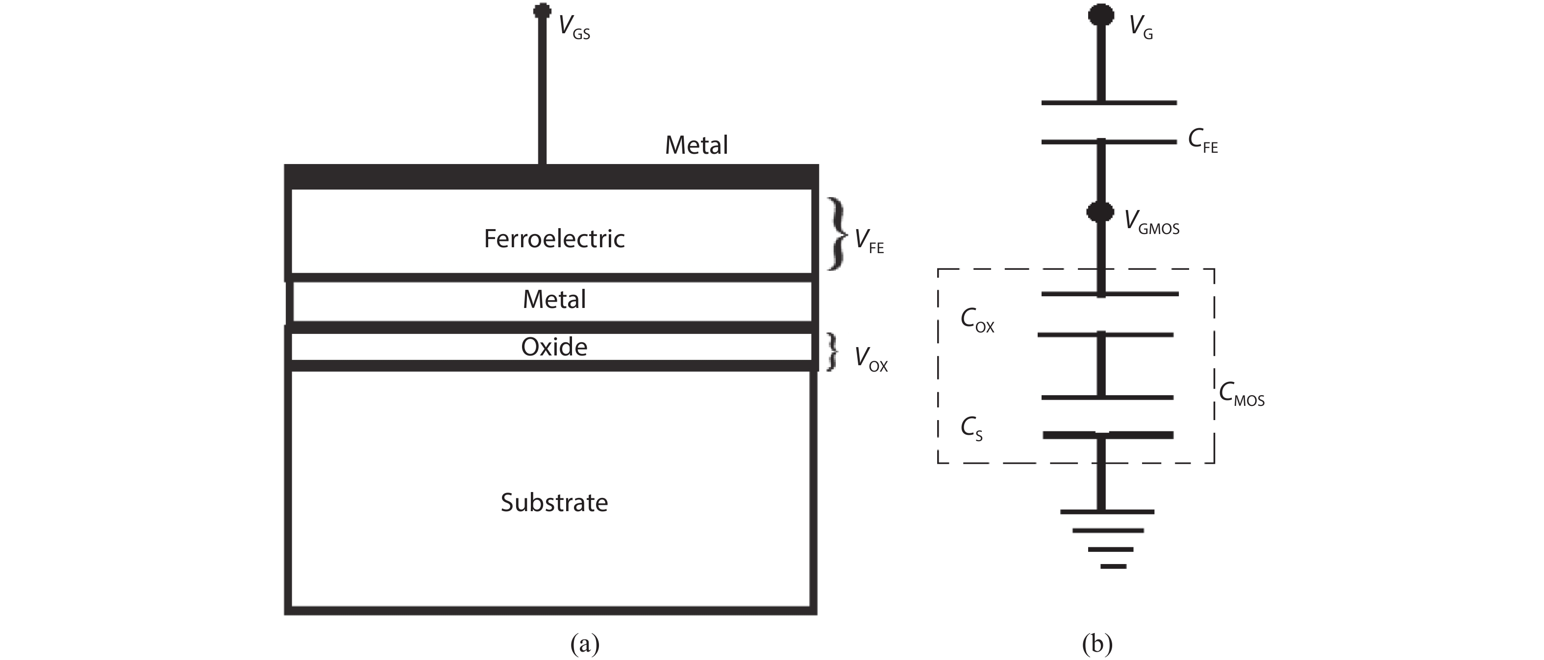
For the analytical analysis of our model, we have considered a basic MOS capacitor with an extra ferroelectric layer in the gate stack. A schematic of a Metal-Ferroelectric-Metal-Insulator-Substrate (MFMIS) negative capacitance capacitor[
![]()
Figure 1.(a) Schematic of MFMIS based NC-FET. (b) Equivalent capacitance divider.
The SS can be reduced by reducing any of the two m or n factors. In the case of the NC capacitor, we are only concerned with the reduction of m to decrease the SS. The factor,
The unique property of NC effect in an MFMIS structure is to provide an internal voltage (VGMOS) that is greater than the applied gate voltage (VGS). From the capacitor divider formed in Fig. 1(b), the partial derivative of the VGS with respect to VGMOS, also known as body factor m, can be written as
where
To include the model for the dynamics of ferroelectric capacitor, the Landau Khalatnikov (LK) equation[
where α, β, γ are known as Landau parameters of the material. Furthermore, α < 0, β > 0, γ ≥ 0 defines the negative capacitance property, VFE is the voltage drop across the ferroelectric film and tFE is the thickness of the ferroelectric layer. The total charge Q is the same as the total charge in the channel, which is calculated using the depletion width approximation and has already explained in Ref. [10]. The potential balance in the equivalent capacitor network results in applied gate voltage VGS as the sum of the voltage drop across the ferroelectric capacitor (VFE) and the internal node voltage VGMOS is given as
where
The total gate capacitance CT of the NC capacitor is given by
The increased gate capacitance due to CFE of the ferroelectric layer in the gate stack, amplifies the internal node voltage. However, CT must be positive for all charges for a hysteresis free stable operation of the device[
which should hold throughout the NC regime. Eq. (7) puts a minimum limit on the subthreshold swing that can be obtained in an NC-FET. For a given dependence of CMOS and CFE on Q, minimum SS can be obtained where the two capacitances match as closely as possible[
For a fixed COX, CMOS changes with CS which depend on the channel doping NA; however, CS depends on whether the channel is in subthreshold, where
Unlike conventional MOSFETs, where the minimum value of SS is fixed at 60 mV/dec, there is no such single value in NC-FET. The minimum subthreshold swing (Smin) that characterizes the NC-FET is different for different devices. However, the two necessary conditions for minimum subthreshold swing are a)
Mathematically, the condition for being in subthreshold is given by
where
Condition (7) is general and will work irrespective of values of CMOS and |CFE|. However, Eq. (8) changes as we change the FET structure, such as single gate versus multigate[
3. Optimal ferroelectric thickness
Fig. 2 shows the VFE–Q characteristics of the ferroelectric material. VFE decreases in the range of –Q1 < Q < + Q1 and hence CFE is also negative between –Q1 and + Q1. However, an n-channel NC-FET must be operated in the Q > 0 branch of the NC regime, so that it can be balanced by the negative charges of the channel. Therefore,
![]()
Figure 2.Voltage-charge plot for a ferroelectric material.
where vt = KBT/q is the thermal voltage. Therefore, the condition in Eq. (7) for minimum subthreshold swing and hysteresis free operation of the device can be translated into
which relates tFE,
The final equation for the optimized ferroelectric thickness is
Thus, for a given ferroelectric material characterized by α, β, and γ, SS is minimized for NA and tFE given by Eqs. (11) and (12). It is clear from this equation that the thickness of ferroelectric material required depends on the landau parameter α of the material and the capacitance of the oxide between the ferroelectric and the silicon substrate. It is evident that high value of parameter α reduces the optimal ferroelectric thickness for a minimum subthreshold swing.
4. Dependence on coercive field (EC) and remnant polarization (P0)
The anisotropy constants α and β in Landau equation are calculated by fitting the Q–VFE characteristics to yield the given value of coercive field EC and the remnant polarization P0. Hence,
Therefore, the thickness of the ferroelectric film in terms of coercive field and remnant polarization can be obtained as
the high coercive field and small remnant polarization results in small tFE.
Ignoring the higher terms of Q in the Eq. (5), the ferroelectric negative capacitance equation reduces to
In an NCFET device, the improved ION/IOFF ratio and small subthreshold swing without hysteresis in the transfer characteristics depends on the capacitance matching (|CFE| > CMOS) or |CFE| ≈ CMOS as already discussed[
![]()
Figure 3.(a) Capacitance versus charge plots for MOS capacitor, ferroelectric capacitor and the total capacitance of MFMIS capacitor. (b) Voltage charge plot of the MFMIS capacitor.
The higher values of CFE due to smaller alpha is due to small EC and large P0 for fixed ferroelectric thickness, which results in lower voltage step up
Similarly, high values of α implies a proportionally low value of |CFE| for a fixed tFE. This can also be understood in terms of very high coercive field and low remnant polarization. The higher values of αresults in the smaller |CFE| than CMOS, results in total negative capacitance which appears as the hysteresis in the transfer characteristics of the devices[
Consequently, we come to the conclusion that in an NC capacitor using ferroelectric material, the material parameters and the thickness of the material are interdependent to achieving a good result.
Considering Eq. (14), a high P0 and low EC results in higher tFE; whereas, a low P0 and high EC results in smaller tFE. The calculated values of tFE can be used to stabilise the capacitance and enhance the capacitance matching to the obtain the best possible results with high ION and no hysteresis. Therefore, we can opt for either higher polarization and smaller EC or higher EC with smaller P0. However, from the design perspective of the NC-FET as experimentally shown in Ref. [20], the gate stack with ferroelectric material giving high EC and low P0 resulted in 45% higher ION with the same OFF current. Therefore, we can say that higher alpha and consequently lower tFE results in better characteristics and are also viable from the point of view of scaling these devices.
5. Equation for minimum subthreshold swing
Unlike Smin = 60 mV/dec for classical FETs, a single Smin does not define the performance of all NCFETs; instead the stability constrained Smin depends on the choice of material system and channel type. In this section, an explicit analytical equation has been obtained to calculate the minimum possible SS (Smin) under capacitance matching conditions. From the calculated Smin for different materials, we can infer the viability of different materials for the designing of NC-FETs.
For a given ferroelectric material characterised by α, β and γ subthreshold swing is minimized for NA and tFE given in Eqs. (11) and (12). The equation for minimum subthreshold swing (Smin) is obtained by substituting the value of CFE in Eq. (2) and can be written as
where
6. Conclusion
In this paper, we have developed an analytical equation for the ferroelectric thickness and the minimum subthreshold swing possible in an MFMIS capacitor. This captures the impact of ferroelectric material properties on the Landau coefficients, which in turn determines the thickness of the ferroelectric material required to have better capacitance matching and which reduces the subthreshold swing. Finally, this study calculated the minimum subthreshold swing of an NC capacitor with five different ferroelectric materials, which may help us in the selection of a particular ferroelectric material for an actual NC-FET design.
References
[1] S Salahuddin, S Datta. Use of Negative capaciatnce to provide volatge amplification for low power nanoscale devices. Nano Lett, 8, 405(2008).
[2] A I Khan, D Bhowmik, P Yu et al. Experimental evidenceof ferroelectric Negative capacitance in nanoscale heterostructures. Appl Phys Lette, 99, 113501(2011).
[3] A C Seabaugh, Q Zhang. Low-voltage tunnel transistors for beyond CMOS logic. Proc IEEE, 98, 2095(2010).
[4] K Gopalakrishnan, R Woo, C Jungemann et al. Impact ionization MOS (I-MOS) -Part I: Device and circuit simulation. IEEE Trans Electron Devices, 52, 69(2005).
[5] A F Devonshire. Theory of ferrolelctrics. Adv Phys, 3, 85(1954).
[6]
[7] V L Ginzburg. Phase transitions in ferroelctrics: some historical remarks. UFN, 171, 1091(2001).
[8] A Rusu, G A Salvatore, D Jimenez et al. Metal-ferroelectric-metal-oxide semiconductor field effect transistor with sub-60mV/decade subthreshold swing and voltage amplification. IEEE International Electron Devices Meeting, 6.3.1(2010).
[9]
[10] R Rasool, G M Rather, N ud-Din. Analytic model for the electrical properties of negative capacitance metal-ferroelectric-insulator-silicon (MFIS) capacitor. Integrated Ferroelectrics, 185, 93(2017).
[11] A Jain, M A Alam. Prospects of hysterisis free abrupt switching (0 mV/decade) in Landau switches. IEEE Trans Electron Devices, 60, 4269(2013).
[12] A I Khan, C W Yeung, C Hu et al. Ferroelectric negative capacitance MOSFET: Capacitance tuning & antiferroelectric operation. IEDM Tech Dig, 255(2011).
[13] J I Seeger, S B Crary. Analysis and simulation of MOS capacitor feedback for stabilizing electrostatically actuated mechanical devices. Trans Built Environ, 31, 1(1997).
[14] C W Krowne, S W kirchoefer, W Chang et al. Examination of possibility of negative capaciatnce using ferroelectric materials in solid state electronic devices. Nanoletters, 11, 988(2011).
[15] A Jain, M A Alam. Stability constraints define the minimum subthreshold swing of a negative capacitance field-effect transistor. IEEE Trans Electron Devices, 61, 2235(2014).
[16] D Jiménez, E Miranda, A Godoy. Analytic model for the surface potential and drain current in negative capacitance field-effect transistors. IEEE Trans Electron Devices, 57, 2405(2010).
[17] R F Pierret. Semiconductor device fundamentals. Pearson(1995).
[18] S Dasgupta, A Rajashekhar, K Majumdar et al. Sub-KT/Q switching in strong inversion in PbZr0.52Ti0.4O3 gated negative capaciatnce FETs. IEEE J Explor Solid State Comput Devices Circuits, 1, 43(2015).
[19] H Lee, Y Yoon, C Shin. Current voltage model for negative capacitance field effect transistors. IEEE Electron Device Lett, 38, 669(2017).
[20] C I Lin, A I Khan, S Salahuddin et al. Effects of the variation of ferroelectric properties on negative capacitance FET characteristics. IEEE Trans Electron Devices, 63, 2197(2016).
[21] A Cano, D Jimenez. Multidomain ferroelectricity as a limiting factor for voltage amplification in ferroelectric field-effect transistors. Appl Phys Lett, 97, 133509(2010).
[22] T S Boscke, J Muller, D Bruhaus et al. Ferroelectricity in hafnium oxide: CMOS compatible ferroelectric field effect transistors. IEE Electron Devices Meeting, 24(2011).
[23] Y Li, Y Lian, K K Yao et al. Evaluation and optimization of short channel ferroelectric MOSFET for low power circuit application with BSIM4 and Landau theory. Solid State Electron, 114, 17(2015).
[24] A Saeidi, F Jazaeri, I Stolichnov et al. Double-gate negative-capaciatnce MOSFET with PZT gate stack on ultra thin body SOI: An experimentally caliberated simulation study of device performance. IEEE Trans Electron Devices, 63, 4678(2016).


Set citation alerts for the article
Please enter your email address

© Copyright 2018-2021 | Chinese Laser Press. All Rights Reserved 沪ICP备15018463号-20