Journals > > Topics > Detectors
Detectors|124 Article(s)
Detectability of Low Characteristic Aircraft Based on Different Ground-Based Infrared Visual Range Prediction Models
Teng Zhang, Xiaying Meng, Wenqiang Gao, Hongli Wang, and Qinglin Niu
ObjectiveLow signature aircraft adopt active or passive methods to reduce the characteristic difference between themselves and surrounding backgrounds, such as high-temperature component cooling, aerodynamic structure layout optimization, and absorbing coating, which brings great challenges to detection systems. The aerodynamic heating of aircraft is difficult to eliminate, which thus provides a radiant source for the infrared detection system. The development of high sensitivity infrared detectors further promotes the detection of low characteristic aircraft by infrared detection systems. Maximum detection range (MDR) is an important performance indicator of infrared detection systems, which is not only related to the target's infrared radiation characteristics but also closely related to the system's visual range prediction model. At present, most research focuses on analyzing the detectability of targets based on a single visual range prediction model. Especially, with low characteristic aircraft as the research object, there is a lack of research on using multiple visual range prediction models for detectability analysis. Therefore, we take low characteristic aircraft as the research object and conduct research based on multiple visual range prediction models, which can provide theoretical support for the detection and recognition of low characteristic aircraft and detector design.MethodsA fly-wing configuration aircraft was taken as the research object. The surface temperature of the aircraft was predicted using the computational fluid dynamics (CFD) method, based on the assumption of a radiative balance wall. The radiative transfer equation (RTE) was solved through the line of sight (LOS) method, taking into account the situation of light being obstructed by the aircraft's skins. The atmospheric transmittance was borrowed from the MODTRAN software. Three ground-based visual range prediction models were established, including noise equivalent flux density (NEFD), minimum detectable temperature difference (MDTD), and minimum resolvable temperature difference (MRTD) algorithms. Finally, an end-to-end numerical simulation model to predict the MDR and maximum detection zenith angle of fly-wing configuration aircraft was established.Results and DiscussionsFor the fly-wing aircraft, the radiance in the long wave infrared (LWIR, 8-12 μm) band is two orders of magnitude higher than that in the medium infrared wave (MWIR, 3-5 μm) band. The radiation intensity of the back and abdomen of the aircraft is the highest, and the radiance in the side-view observation is basically the same (Fig. 7 and Fig. 8). The MDR of the NEFD visual range prediction model is nearly one order of magnitude higher in the LWIR band than that in the MWIR band. However, the MDR of the MDTD and MRTD models is approximately equal in both bands. In the LWIR band, the MDR and the maximum detection zenith angle calculated by the three visual range prediction models in descending order are as follows: NEFD>MDTD>MRTD. In the MWIR band, the MDR of the MDTD model is the largest compared with the other two models. The MDR of the NEFD model within the detection plane containing pitch angle variation is about 170 km, which is suitable for detecting the back and abdomen of the aircraft. However, the MDTD and MRTD models have the MDRs in the bottom-view observation, with an MDR of 57 km and 38 km, respectively (Fig. 9 and Fig. 10). Within the side-view observation plane, the MDR calculated by the NEFD model is approximately 62 km (Fig. 11 and Fig. 12). Under different observation levels including discovery, classification, and recognition, the low characteristic aircraft can be detected by the MRTD model, but the MRTD model fails to detect such fly-wing aircraft under the identify level (Fig. 14).Conclusions1) The radiance in the LWIR band is two orders of magnitude higher than that in the MWIR band. The radiation intensity in the top-view observation is nearly one order of magnitude higher than that in the side-view observation. It is indicated that infrared radiation intensity has strong selectivity in terms of spectral bands and detection angles. 2) The MDR of the NEFD model in the LWIR band is nearly one order of magnitude higher than that in the MWIR band, and the MDRs of the MDTD and MRTD models in the MWIR band and LWIR band are basically the same. In the LWIR band, the MDRs of the three models are sorted in descending order: NEFD>MDTD>MRTD. 3) In the detection plane of the pitch angle, the MDR of the NEFD model in the top-view and bottom-view is about 170 km, and the MDRs of the MDTD and MRTD models are 57 km and 38 km, respectively. 4) The MRTD model can detect aircraft at discovery, classification, and recognition observation levels, but it is invalid at identify level. ObjectiveLow signature aircraft adopt active or passive methods to reduce the characteristic difference between themselves and surrounding backgrounds, such as high-temperature component cooling, aerodynamic structure layout optimization, and absorbing coating, which brings great challenges to detection systems. The aerodynamic heating of aircraft is difficult to eliminate, which thus provides a radiant source for the infrared detection system. The development of high sensitivity infrared detectors further promotes the detection of low characteristic aircraft by infrared detection systems. Maximum detection range (MDR) is an important performance indicator of infrared detection systems, which is not only related to the target's infrared radiation characteristics but also closely related to the system's visual range prediction model. At present, most research focuses on analyzing the detectability of targets based on a single visual range prediction model. Especially, with low characteristic aircraft as the research object, there is a lack of research on using multiple visual range prediction models for detectability analysis. Therefore, we take low characteristic aircraft as the research object and conduct research based on multiple visual range prediction models, which can provide theoretical support for the detection and recognition of low characteristic aircraft and detector design.MethodsA fly-wing configuration aircraft was taken as the research object. The surface temperature of the aircraft was predicted using the computational fluid dynamics (CFD) method, based on the assumption of a radiative balance wall. The radiative transfer equation (RTE) was solved through the line of sight (LOS) method, taking into account the situation of light being obstructed by the aircraft's skins. The atmospheric transmittance was borrowed from the MODTRAN software. Three ground-based visual range prediction models were established, including noise equivalent flux density (NEFD), minimum detectable temperature difference (MDTD), and minimum resolvable temperature difference (MRTD) algorithms. Finally, an end-to-end numerical simulation model to predict the MDR and maximum detection zenith angle of fly-wing configuration aircraft was established.Results and DiscussionsFor the fly-wing aircraft, the radiance in the long wave infrared (LWIR, 8-12 μm) band is two orders of magnitude higher than that in the medium infrared wave (MWIR, 3-5 μm) band. The radiation intensity of the back and abdomen of the aircraft is the highest, and the radiance in the side-view observation is basically the same (Fig. 7 and Fig. 8). The MDR of the NEFD visual range prediction model is nearly one order of magnitude higher in the LWIR band than that in the MWIR band. However, the MDR of the MDTD and MRTD models is approximately equal in both bands. In the LWIR band, the MDR and the maximum detection zenith angle calculated by the three visual range prediction models in descending order are as follows: NEFD>MDTD>MRTD. In the MWIR band, the MDR of the MDTD model is the largest compared with the other two models. The MDR of the NEFD model within the detection plane containing pitch angle variation is about 170 km, which is suitable for detecting the back and abdomen of the aircraft. However, the MDTD and MRTD models have the MDRs in the bottom-view observation, with an MDR of 57 km and 38 km, respectively (Fig. 9 and Fig. 10). Within the side-view observation plane, the MDR calculated by the NEFD model is approximately 62 km (Fig. 11 and Fig. 12). Under different observation levels including discovery, classification, and recognition, the low characteristic aircraft can be detected by the MRTD model, but the MRTD model fails to detect such fly-wing aircraft under the identify level (Fig. 14).Conclusions1) The radiance in the LWIR band is two orders of magnitude higher than that in the MWIR band. The radiation intensity in the top-view observation is nearly one order of magnitude higher than that in the side-view observation. It is indicated that infrared radiation intensity has strong selectivity in terms of spectral bands and detection angles. 2) The MDR of the NEFD model in the LWIR band is nearly one order of magnitude higher than that in the MWIR band, and the MDRs of the MDTD and MRTD models in the MWIR band and LWIR band are basically the same. In the LWIR band, the MDRs of the three models are sorted in descending order: NEFD>MDTD>MRTD. 3) In the detection plane of the pitch angle, the MDR of the NEFD model in the top-view and bottom-view is about 170 km, and the MDRs of the MDTD and MRTD models are 57 km and 38 km, respectively. 4) The MRTD model can detect aircraft at discovery, classification, and recognition observation levels, but it is invalid at identify level.
Acta Optica Sinica
- Publication Date: Mar. 10, 2024
- Vol. 44, Issue 6, 0604001 (2024)

Multi-Pixel Balanced Homodyne Detector
Shaofeng Wang, Hanqing Li, Kangkang Li, Peng Liu, Juan Li, and Ruifang Dong
ObjectiveAs an important tool for quantum optical measurement, the balanced homodyne detector (BHD) is highly sensitive to the amplitude and phase of the incident light. It can reliably extract quantum fluctuations, suppress classical common-mode noise, and amplify quantum fluctuations to the macro level. Additionally, it has been widely employed in quantum noise measurement, gravitational wave detection, high-sensitivity interferometric timing measurement, continuous variable quantum key distribution, and quantum random number generator. The common-mode rejection ratio (CMRR), operating bandwidth, and signal-to-noise ratio (SNR) of the detector have been the research focuses. The optical frequency comb contains a large number of equally spaced longitudinal modes, which is a good multi-mode resource. The spectrum width of the optical frequency comb is in the order of nanometers. The quantum optical frequency comb which breaks the limit of shot noise can be generated by nonlinear processes. Quantum optical frequency comb has a great application prospect in quantum precision measurement. Spectrally resolved balanced homodyne detection is an important detection method of quantum optical frequency comb. We analyze the noise source of the balanced homodyne detector theoretically and design the multi-pixel balanced homodyne detector (MBHD) based on photodiode array and multi-channel inductance-capacitance (L-C) coupled transimpedance amplifier (TIA) circuit. These designs enable MBHD to meet multi-channel parallel and high-SNR quantum noise measurements.MethodsThe MBHD consists of two highly symmetrical multi-pixel photodetectors (MPDs) and a multi-channel subtracter (Fig. 1). Each MPD includes a photodiode array, a multi-channel L-C coupled structure, AC amplification, and DC amplification. The photocurrent generated by the corresponding pair of pixels in the two MPD flows through their respective AC amplification outputs, and the common-mode signal in the detection result is eliminated by the subtracter to complete the multi-pixel parallel balanced homodyne detection. Multi-channel DC output monitors the optical power of all pixels by a multi-function data acquisition card (DAQ). In the amplification circuit structure of the single pixel in MPD, the generated photocurrent signal is divided into DC signal and AC signal through the L-C coupled circuit. The AC signal is converted into a voltage signal by a TIA and is further adopted to measure the intensity noise power of the incident light. The DC signal is converted into a voltage signal by a load resistor and a isolation amplifier. Additionally, an equivalent noise model is built to analyze the electronic noise. Due to the multi-channel parallel structure of the MBHD, each channel is similar to each other and independent. The electronic noise of the single-pixel channel includes the noise generated by the dark current of the photodiode, the thermal noise generated by the feedback resistance in the transimpedance amplifier circuit, the noise generated by the input voltage noise of the transimpedance amplifier, and the noise generated by the input current noise of the transimpedance amplifier. Theoretical analysis shows that a reasonable selection of feedback resistance and inductance, photodiode with low dark current and low junction capacitance, and the TIA with low input noise can reduce the electronic noise of the detector. Meanwhile, the L-C coupled structure is better than the R-C coupled structure in experimental conditions (Fig. 2).Results and DiscussionsThe device is constructed to test the performance of MBHD (Fig. 3). AC output of MBHD is connected to a spectrometer to measure the bandwidth and SNR. The DC signals of each pixel are measured by a DAQ to monitor the optical powers of each pixel. When the optical power is distributed on all pixel channels, the distribution of the shot noise power in each channel is proportional to the distribution of the incident optical power, which verifies that the multi-pixel BHD can achieve spectrally resolved multi-channel parallel balanced homodyne detection (Fig. 4). When the incident optical power is 1.660 mW, 0.834 mW, 0.418 mW, 0.208 mW, and 0.102 mW respectively, the shot noise spectrum and electronic noise spectrum of one pixel are measured at different analysis frequencies (Fig. 5). The test results show that the 3 dB bandwidth of MBHD is 5 MHz. The resolution bandwidth is set to 100 kHz, the video bandwidth is 100 Hz, and the number of averaging times is 10. When the incident optical power is 1.660 mW, the shot noise power is 23 dB higher than the electronic noise power at the analysis frequency of 2 MHz. By comparing the shot noise power under different incident optical power, the shot noise power decreases by 3 dB when the incident optical power decreases by half, which indicates that the detector has a good linear gain within 0.102 mW to 1.660 mW of the optical power.ConclusionsBased on the noise model of the BHD, the electronic noise source is analyzed theoretically. The results indicate that the L-C coupled structure is better. By adopting the multi-pixel photodiode array and L-C coupled structure, a high-performance multi-pixel BHD is developed. In each pixel channel, when the 815 nm laser with optical power of 1.660 mW is incident, the shot noise power is 23 dB higher than the electronic noise at the analysis frequency of 2 MHz. By employing the grating to scatter the incident light horizontally, the shot noise power in each channel is proportional to the incident optical power. It is verified that the multi-pixel BHD can realize the spectrally resolved multi-channel parallel balanced homodyne detection. The detector provides a high-performance detection tool for quantum precision measurement based on quantum optical frequency comb. ObjectiveAs an important tool for quantum optical measurement, the balanced homodyne detector (BHD) is highly sensitive to the amplitude and phase of the incident light. It can reliably extract quantum fluctuations, suppress classical common-mode noise, and amplify quantum fluctuations to the macro level. Additionally, it has been widely employed in quantum noise measurement, gravitational wave detection, high-sensitivity interferometric timing measurement, continuous variable quantum key distribution, and quantum random number generator. The common-mode rejection ratio (CMRR), operating bandwidth, and signal-to-noise ratio (SNR) of the detector have been the research focuses. The optical frequency comb contains a large number of equally spaced longitudinal modes, which is a good multi-mode resource. The spectrum width of the optical frequency comb is in the order of nanometers. The quantum optical frequency comb which breaks the limit of shot noise can be generated by nonlinear processes. Quantum optical frequency comb has a great application prospect in quantum precision measurement. Spectrally resolved balanced homodyne detection is an important detection method of quantum optical frequency comb. We analyze the noise source of the balanced homodyne detector theoretically and design the multi-pixel balanced homodyne detector (MBHD) based on photodiode array and multi-channel inductance-capacitance (L-C) coupled transimpedance amplifier (TIA) circuit. These designs enable MBHD to meet multi-channel parallel and high-SNR quantum noise measurements.MethodsThe MBHD consists of two highly symmetrical multi-pixel photodetectors (MPDs) and a multi-channel subtracter (Fig. 1). Each MPD includes a photodiode array, a multi-channel L-C coupled structure, AC amplification, and DC amplification. The photocurrent generated by the corresponding pair of pixels in the two MPD flows through their respective AC amplification outputs, and the common-mode signal in the detection result is eliminated by the subtracter to complete the multi-pixel parallel balanced homodyne detection. Multi-channel DC output monitors the optical power of all pixels by a multi-function data acquisition card (DAQ). In the amplification circuit structure of the single pixel in MPD, the generated photocurrent signal is divided into DC signal and AC signal through the L-C coupled circuit. The AC signal is converted into a voltage signal by a TIA and is further adopted to measure the intensity noise power of the incident light. The DC signal is converted into a voltage signal by a load resistor and a isolation amplifier. Additionally, an equivalent noise model is built to analyze the electronic noise. Due to the multi-channel parallel structure of the MBHD, each channel is similar to each other and independent. The electronic noise of the single-pixel channel includes the noise generated by the dark current of the photodiode, the thermal noise generated by the feedback resistance in the transimpedance amplifier circuit, the noise generated by the input voltage noise of the transimpedance amplifier, and the noise generated by the input current noise of the transimpedance amplifier. Theoretical analysis shows that a reasonable selection of feedback resistance and inductance, photodiode with low dark current and low junction capacitance, and the TIA with low input noise can reduce the electronic noise of the detector. Meanwhile, the L-C coupled structure is better than the R-C coupled structure in experimental conditions (Fig. 2).Results and DiscussionsThe device is constructed to test the performance of MBHD (Fig. 3). AC output of MBHD is connected to a spectrometer to measure the bandwidth and SNR. The DC signals of each pixel are measured by a DAQ to monitor the optical powers of each pixel. When the optical power is distributed on all pixel channels, the distribution of the shot noise power in each channel is proportional to the distribution of the incident optical power, which verifies that the multi-pixel BHD can achieve spectrally resolved multi-channel parallel balanced homodyne detection (Fig. 4). When the incident optical power is 1.660 mW, 0.834 mW, 0.418 mW, 0.208 mW, and 0.102 mW respectively, the shot noise spectrum and electronic noise spectrum of one pixel are measured at different analysis frequencies (Fig. 5). The test results show that the 3 dB bandwidth of MBHD is 5 MHz. The resolution bandwidth is set to 100 kHz, the video bandwidth is 100 Hz, and the number of averaging times is 10. When the incident optical power is 1.660 mW, the shot noise power is 23 dB higher than the electronic noise power at the analysis frequency of 2 MHz. By comparing the shot noise power under different incident optical power, the shot noise power decreases by 3 dB when the incident optical power decreases by half, which indicates that the detector has a good linear gain within 0.102 mW to 1.660 mW of the optical power.ConclusionsBased on the noise model of the BHD, the electronic noise source is analyzed theoretically. The results indicate that the L-C coupled structure is better. By adopting the multi-pixel photodiode array and L-C coupled structure, a high-performance multi-pixel BHD is developed. In each pixel channel, when the 815 nm laser with optical power of 1.660 mW is incident, the shot noise power is 23 dB higher than the electronic noise at the analysis frequency of 2 MHz. By employing the grating to scatter the incident light horizontally, the shot noise power in each channel is proportional to the incident optical power. It is verified that the multi-pixel BHD can realize the spectrally resolved multi-channel parallel balanced homodyne detection. The detector provides a high-performance detection tool for quantum precision measurement based on quantum optical frequency comb.
Acta Optica Sinica
- Publication Date: Mar. 10, 2024
- Vol. 44, Issue 5, 0504002 (2024)
Optimal Design of Charge-Free Layer InGaAs/Si Avalanche Photodetector
Juan Zhang, Er Yao, and Shaoying Ke
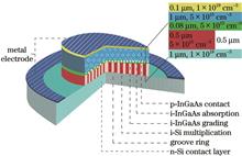
ObjectiveInGaAs/Si avalanche photodiode (APD) employs Si materials with extremely low electron hole ionization coefficients as the multiplication layer, which to some extent solves the problem of high equivalent noise. However, its manufacturing involves ion implantation of Si charge layer and high-temperature annealing activation, which features a complex process, uneven impurities distribution, and high cost. We propose the utilization of etching technology to prepare groove rings in the Si multiplication layer and fill different media in the groove rings to modulate the electric field in the InGaAs layer and Si layer, thus building a charge-free layer InGaAs/Si APD device model. The results indicate that filling the groove ring with air or SiO2 can achieve high-performance InGaAs/Si APD. Finally, theoretical guidance can be provided for the subsequent development of InGaAs/Si APD with simple processes, stable performance, and low noise.MethodsWe propose to adopt etching technology to prepare a groove ring within the Si multiplication layer and fill different media inside the groove ring to modulate the electric field in the InGaAs layer and Si layer, which helps build a charge-free layer InGaAs/Si APD device model. Firstly, the changes in APD optical and dark current with different media are simulated. The changes in recombination rate and carrier concentration are simulated to explore the reasons for the changes in optical current. Secondly, the energy band changes of the APD are simulated to further understand the reasons for electron concentration changes. Thirdly, the changes of charge concentration, impact ionization rate, electric field, and other parameters with different media are simulated. Finally, the gain, bandwidth, and gain-bandwidth product of APD are simulated, and a comparison of different media shows that filling with the air can yield the best device performance.Results and DiscussionsThe overall trend of optical current and dark current decreases with the increasing dielectric constant of the medium (Fig. 2). As the dielectric constant of the medium rises, the recombination rate decreases in the InGaAs absorption layer, Si multiplication layer, and Si substrate, consistent with the trend of optical current variation (Fig. 3). The conduction band of APD has no band order at the bonding interface, while the valence band at the interface has obvious band orders, making it difficult for carriers to transport at the interface and a large number of holes to accumulate at the interface (Fig. 5). The ionization coefficients of electrons and holes in the absorption layer slowly increase, while the ionization coefficients of electrons and holes in the multiplication layer further decrease, which is consistent with the trend of electric field changes (Fig. 7). As the dielectric constant increases, the electric field strength in the multiplication region gradually reduces, which weakens the carrier impact ionization effect and decreases the gain (Fig. 8). When the bias voltage is 35 V, the gain-bandwidth product basically shows a downward trend with the increasing dielectric constant of the medium. Additionally, when the medium inside the groove ring is air and the reverse bias voltage is equal to the avalanche voltage (35.2 V), the gain-bandwidth product reaches 100 GHz (Fig. 11).ConclusionsWe investigate the effect of filling different media in the Si multiplication layer groove ring on the charge-free layer InGaAs/Si APD. The results show that as the dielectric constant of different media increases, both optical current and dark current present a decreasing trend under the same bias voltage. The InGaAs/Si APD with air or SiO2 as the dielectric materials finally overlaps with the optical current and dark current after reaching the avalanche voltage, exhibiting the best current characteristics. As the dielectric constant of the medium rises, the gain-bandwidth product shows a downward trend under the same bias voltage. After the device avalanche, the gain-bandwidth product exhibits a trend of first increasing and then decreasing. When the medium inside the groove ring is air and the reverse bias voltage is 35.2 V, the gain-bandwidth product reaches 100 GHz. In summary, replacing the charge layer with a groove ring to construct a charge-free layer InGaAs/Si APD does not require ion implantation, and the process is simple. Meanwhile, filling the groove ring with air can yield the best device performance, and this new configuration provides a new idea for designing high-performance InGaAs/Si APD with simple processes. ObjectiveInGaAs/Si avalanche photodiode (APD) employs Si materials with extremely low electron hole ionization coefficients as the multiplication layer, which to some extent solves the problem of high equivalent noise. However, its manufacturing involves ion implantation of Si charge layer and high-temperature annealing activation, which features a complex process, uneven impurities distribution, and high cost. We propose the utilization of etching technology to prepare groove rings in the Si multiplication layer and fill different media in the groove rings to modulate the electric field in the InGaAs layer and Si layer, thus building a charge-free layer InGaAs/Si APD device model. The results indicate that filling the groove ring with air or SiO2 can achieve high-performance InGaAs/Si APD. Finally, theoretical guidance can be provided for the subsequent development of InGaAs/Si APD with simple processes, stable performance, and low noise.MethodsWe propose to adopt etching technology to prepare a groove ring within the Si multiplication layer and fill different media inside the groove ring to modulate the electric field in the InGaAs layer and Si layer, which helps build a charge-free layer InGaAs/Si APD device model. Firstly, the changes in APD optical and dark current with different media are simulated. The changes in recombination rate and carrier concentration are simulated to explore the reasons for the changes in optical current. Secondly, the energy band changes of the APD are simulated to further understand the reasons for electron concentration changes. Thirdly, the changes of charge concentration, impact ionization rate, electric field, and other parameters with different media are simulated. Finally, the gain, bandwidth, and gain-bandwidth product of APD are simulated, and a comparison of different media shows that filling with the air can yield the best device performance.Results and DiscussionsThe overall trend of optical current and dark current decreases with the increasing dielectric constant of the medium (Fig. 2). As the dielectric constant of the medium rises, the recombination rate decreases in the InGaAs absorption layer, Si multiplication layer, and Si substrate, consistent with the trend of optical current variation (Fig. 3). The conduction band of APD has no band order at the bonding interface, while the valence band at the interface has obvious band orders, making it difficult for carriers to transport at the interface and a large number of holes to accumulate at the interface (Fig. 5). The ionization coefficients of electrons and holes in the absorption layer slowly increase, while the ionization coefficients of electrons and holes in the multiplication layer further decrease, which is consistent with the trend of electric field changes (Fig. 7). As the dielectric constant increases, the electric field strength in the multiplication region gradually reduces, which weakens the carrier impact ionization effect and decreases the gain (Fig. 8). When the bias voltage is 35 V, the gain-bandwidth product basically shows a downward trend with the increasing dielectric constant of the medium. Additionally, when the medium inside the groove ring is air and the reverse bias voltage is equal to the avalanche voltage (35.2 V), the gain-bandwidth product reaches 100 GHz (Fig. 11).ConclusionsWe investigate the effect of filling different media in the Si multiplication layer groove ring on the charge-free layer InGaAs/Si APD. The results show that as the dielectric constant of different media increases, both optical current and dark current present a decreasing trend under the same bias voltage. The InGaAs/Si APD with air or SiO2 as the dielectric materials finally overlaps with the optical current and dark current after reaching the avalanche voltage, exhibiting the best current characteristics. As the dielectric constant of the medium rises, the gain-bandwidth product shows a downward trend under the same bias voltage. After the device avalanche, the gain-bandwidth product exhibits a trend of first increasing and then decreasing. When the medium inside the groove ring is air and the reverse bias voltage is 35.2 V, the gain-bandwidth product reaches 100 GHz. In summary, replacing the charge layer with a groove ring to construct a charge-free layer InGaAs/Si APD does not require ion implantation, and the process is simple. Meanwhile, filling the groove ring with air can yield the best device performance, and this new configuration provides a new idea for designing high-performance InGaAs/Si APD with simple processes.
Acta Optica Sinica
- Publication Date: Mar. 10, 2024
- Vol. 44, Issue 5, 0504001 (2024)
P3HT∶Y6-Based Near-Infrared Organic Photomultiplication Photodetectors by Intermolecular Charge Transfer Effects
Yifan Hu, Yulu Hua, Ting Ji, Linlin Shi, Yanxia Cui, and Guohui Li
ObjectiveThe photomultiplication organic photodetector based on trap-assisted carrier tunneling mechanism not only has high sensitivity but also simplifies system design and effectively improves the weak light detection performance of the photodetector. At present, photomultiplication organic photodetectors mainly focus on the visible range and have relatively few responses in the near-infrared region. Detection in the near-infrared region has broad application prospects in many fields and the demand is becoming increasingly urgent. Intermolecular charge transfer is a low-cost method for achieving near-infrared absorption in organic photomultiplier detectors, which can effectively expand the response band of devices. However, the absorption is low and the response is very weak at long wavelengths. The photomultiplication type devices can amplify weak photocurrent signals and improve device performance. Therefore, by introducing a small amount of organic acceptor Y6 in the P3HT active layer, we fabricate a photomultiplication type organic photodetector. Due to the intermolecular charge transfer between P3HT and Y6, the response band of the device can be extended to 1310 nm, which is superior to the reported near-infrared multiplication type organic photodetectors. By introducing an atomic level thickness of Al2O3 between the hole transport layer and the active layer, the device can work under both positive and negative biases. The external quantum efficiency of the device at 860 nm reaches 800%, with a detectivity of 5.6×10¹¹ Jones. The external quantum efficiency of the device at 1310 nm reaches 80.4%, and the specific detectivity reaches 5.13×10¹⁰ Jones. This work can promote the development of near-infrared photomultiplication organic photodetector.MethodsFirstly, the cleaned ITO substrates are dried by nitrogen gas and transferred to a glove box. PEDOT∶PSS is diluted with anhydrous ethanol in a volume ratio of 1∶9 and is span-coated onto the ITO substrate to form a hole transport layer. Then, the Al2O3 interface modification layer is deposited by atomic layer deposition equipment. Subsequently, the active layer is formed by spin-coating P3HT∶Y6 mixture solution, with a P3HT and Y6 ratio of 100∶1 in weight. Finally, the Al electrode is deposited on the active layer by thermal evaporation. The bright and dark currents of the device are obtained by a digital source meter Keithley 2400 and different light sources in a sealed and room temperature state. The testing of external quantum efficiency and responsiveness is performed in a dark shielding box, with ITO as the anode connecting to the positive pole of the power supply and Al as the cathode connecting to the negative pole. The digital source meter Keithley 2400 is adopted to apply different voltages, and a femtosecond laser is utilized as the light source. The light intensity is attenuated to a specified size by an attenuation plate, and the dark current and bright state J-V curves under different light sources are collected. Finally, the external quantum efficiency and responsivity data are obtained through calculation (the data has been background deducted). The linear dynamic range, noise current, and specific detection rate of the device are tested, and the performance of the device is comprehensively analyzed. A spectrophotometer instrument is leveraged to characterize the ultraviolet visible near-infrared absorption spectrum. In addition, the transmission spectrum, reflection spectrum, and film thickness of the device are also tested.Results and DiscussionsAl2O3 modified device with a structure of ITO/PEDOT∶PSS/Al2O3/P3HT∶Y6 (100∶1)/Al and a control device without Al2O3 are both fabricated. We verify that the Al2O3 interface modification layer can greatly reduce the dark current of the device and enable the device to achieve bidirectional bias response (Fig. 1). Next, the Al2O3 modified device is characterized, and the device can respond to 1310 nm. The weak light detection limit of the device at 505 nm can reach 7.8 nW/cm2. When the optical power density is 3.8×10⁻⁴ mW/cm2, the external quantum efficiency of the device at 860 nm is 800%, with a specific detectivity of 5.6×10¹¹ Jones. When the optical power density is 3.67×10⁻² mW/cm2, the external quantum efficiency of the device at 1310 nm is 80.4%, with a specific detectivity of 5.13×10¹⁰ Jones. Under the irradiation of visible light at 505 nm and near-infrared light at 860 nm, the device has a dynamic range of over 125 dB and 90 dB, respectively (Fig. 2 and Fig. 3). The comprehensive performance of the device has certain advantages compared to the near-infrared organic photomultiplier detectors prepared in recent years. By introducing an organic receptor Y6 with light absorption ability in the near-infrared region, the device effectively promotes the injection of holes from external currents as an electron trap and interacts with P3HT, expanding the corresponding band and achieving high sensitivity detection in the near-infrared region (Fig. 4).ConclusionsA low-cost and highly sensitive near-infrared photomultiplication organic photodetector with a structure of ITO/PEDOT∶PSS/Al2O3/P3HT∶Y6/Al is reported. By adding Al2O3 as an interface modification layer, the dark current of the device is significantly reduced, resulting in a device that can respond in both forward and reverse bias directions. Adding a small amount of Y6 to the active layer can achieve a wide spectral response from UV visible to near-infrared, and the response wavelength can be extended to 1310 nm. The external quantum efficiency of the device at 860 nm reaches 800%, with a specific detectivity of 5.6×10¹¹ Jones. The external quantum efficiency of the device at 1310 nm reaches 80.4%, and the specific detectivity reaches 5.13×10¹⁰ Jones. These properties have certain advantages in reported near-infrared photomultiplication organic photodetector and can promote the development of near-infrared photomultiplication organic photodetectors. ObjectiveThe photomultiplication organic photodetector based on trap-assisted carrier tunneling mechanism not only has high sensitivity but also simplifies system design and effectively improves the weak light detection performance of the photodetector. At present, photomultiplication organic photodetectors mainly focus on the visible range and have relatively few responses in the near-infrared region. Detection in the near-infrared region has broad application prospects in many fields and the demand is becoming increasingly urgent. Intermolecular charge transfer is a low-cost method for achieving near-infrared absorption in organic photomultiplier detectors, which can effectively expand the response band of devices. However, the absorption is low and the response is very weak at long wavelengths. The photomultiplication type devices can amplify weak photocurrent signals and improve device performance. Therefore, by introducing a small amount of organic acceptor Y6 in the P3HT active layer, we fabricate a photomultiplication type organic photodetector. Due to the intermolecular charge transfer between P3HT and Y6, the response band of the device can be extended to 1310 nm, which is superior to the reported near-infrared multiplication type organic photodetectors. By introducing an atomic level thickness of Al2O3 between the hole transport layer and the active layer, the device can work under both positive and negative biases. The external quantum efficiency of the device at 860 nm reaches 800%, with a detectivity of 5.6×10¹¹ Jones. The external quantum efficiency of the device at 1310 nm reaches 80.4%, and the specific detectivity reaches 5.13×10¹⁰ Jones. This work can promote the development of near-infrared photomultiplication organic photodetector.MethodsFirstly, the cleaned ITO substrates are dried by nitrogen gas and transferred to a glove box. PEDOT∶PSS is diluted with anhydrous ethanol in a volume ratio of 1∶9 and is span-coated onto the ITO substrate to form a hole transport layer. Then, the Al2O3 interface modification layer is deposited by atomic layer deposition equipment. Subsequently, the active layer is formed by spin-coating P3HT∶Y6 mixture solution, with a P3HT and Y6 ratio of 100∶1 in weight. Finally, the Al electrode is deposited on the active layer by thermal evaporation. The bright and dark currents of the device are obtained by a digital source meter Keithley 2400 and different light sources in a sealed and room temperature state. The testing of external quantum efficiency and responsiveness is performed in a dark shielding box, with ITO as the anode connecting to the positive pole of the power supply and Al as the cathode connecting to the negative pole. The digital source meter Keithley 2400 is adopted to apply different voltages, and a femtosecond laser is utilized as the light source. The light intensity is attenuated to a specified size by an attenuation plate, and the dark current and bright state J-V curves under different light sources are collected. Finally, the external quantum efficiency and responsivity data are obtained through calculation (the data has been background deducted). The linear dynamic range, noise current, and specific detection rate of the device are tested, and the performance of the device is comprehensively analyzed. A spectrophotometer instrument is leveraged to characterize the ultraviolet visible near-infrared absorption spectrum. In addition, the transmission spectrum, reflection spectrum, and film thickness of the device are also tested.Results and DiscussionsAl2O3 modified device with a structure of ITO/PEDOT∶PSS/Al2O3/P3HT∶Y6 (100∶1)/Al and a control device without Al2O3 are both fabricated. We verify that the Al2O3 interface modification layer can greatly reduce the dark current of the device and enable the device to achieve bidirectional bias response (Fig. 1). Next, the Al2O3 modified device is characterized, and the device can respond to 1310 nm. The weak light detection limit of the device at 505 nm can reach 7.8 nW/cm2. When the optical power density is 3.8×10⁻⁴ mW/cm2, the external quantum efficiency of the device at 860 nm is 800%, with a specific detectivity of 5.6×10¹¹ Jones. When the optical power density is 3.67×10⁻² mW/cm2, the external quantum efficiency of the device at 1310 nm is 80.4%, with a specific detectivity of 5.13×10¹⁰ Jones. Under the irradiation of visible light at 505 nm and near-infrared light at 860 nm, the device has a dynamic range of over 125 dB and 90 dB, respectively (Fig. 2 and Fig. 3). The comprehensive performance of the device has certain advantages compared to the near-infrared organic photomultiplier detectors prepared in recent years. By introducing an organic receptor Y6 with light absorption ability in the near-infrared region, the device effectively promotes the injection of holes from external currents as an electron trap and interacts with P3HT, expanding the corresponding band and achieving high sensitivity detection in the near-infrared region (Fig. 4).ConclusionsA low-cost and highly sensitive near-infrared photomultiplication organic photodetector with a structure of ITO/PEDOT∶PSS/Al2O3/P3HT∶Y6/Al is reported. By adding Al2O3 as an interface modification layer, the dark current of the device is significantly reduced, resulting in a device that can respond in both forward and reverse bias directions. Adding a small amount of Y6 to the active layer can achieve a wide spectral response from UV visible to near-infrared, and the response wavelength can be extended to 1310 nm. The external quantum efficiency of the device at 860 nm reaches 800%, with a specific detectivity of 5.6×10¹¹ Jones. The external quantum efficiency of the device at 1310 nm reaches 80.4%, and the specific detectivity reaches 5.13×10¹⁰ Jones. These properties have certain advantages in reported near-infrared photomultiplication organic photodetector and can promote the development of near-infrared photomultiplication organic photodetectors.
Acta Optica Sinica
- Publication Date: Feb. 25, 2024
- Vol. 44, Issue 4, 0404001 (2024)
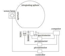
Response Nonlinear Calibration of Solar Blind Phototube Detection System Using Indirect Method
Hanhui Cao, Hongyao Chen, Wenxin Huang, and Jiawei Li
ObjectiveUltraviolet detection technology is widely used in military and civilian fields, playing an important role in missile warning, ultraviolet/infrared composite guidance, detection of solar ultraviolet radiation intensity, ozone detection, biomedicine, and other fields. In recent years, with the development of ultraviolet optical remote sensing detection technology, quantitative research on ultraviolet radiation information has become particularly important. As a type of ultraviolet detector, the solar blind phototube can reduce the impact of out-of-band leakage in ultraviolet radiation measurement, thereby improving the detection accuracy of the ultraviolet band. Based on its characteristics, it is often used in various large military equipment missile approaching warning systems and also commonly used in corona detection to effectively and quickly detect fault locations. In Europe and America, it has been used as a standard power detection method and widely applied in equipment. At present, research on solar blind phototube preparation has gradually begun in China, and the study of its radiation quantification is one of the key links for application. Therefore, in the face of the urgent need for high-precision radiation calibration in the ultraviolet band and the exploration of the application of solar blind photocell, it is necessary to study its response nonlinearity.MethodsThe research on the response nonlinearity of detectors can be divided into two methods:direct method and indirect method. Based on the indirect method, the responsivity standard is transferred to the detector to be calibrated by the standard detector method. The response nonlinearity of the solar blind phototube detection system is studied, and a standard transfer chain based on the detector is established. In terms of the measurement method, we use an external xenon lamp integrating sphere as the radiation source and control the luminous flux of the external xenon lamp entering the integrating sphere through an adjustable aperture. The adjustment of the radiance of the sphere exit portal is achieved and the spectral consistency during the adjustment process is ensured. In this way, the synchronous measurement of the reference detector and the detector to be tested is easy to achieve under the same radiation conditions. In traditional measurement methods, the optical power level of the radiation source is selected with a set of neutral density filters used either one at a time or in combinations of several filters. It needs to construct a dual optical path to achieve synchronous measurement between the reference detector and the detector to be tested. Otherwise, it needs to establish a standard transfer chain by a motor to continuously exchange the positions of the two detectors. Therefore, we provide a new approach for the study of detector response nonlinearity. Compared to traditional measurement methods, the proposed approach simplifies the complexity of the optical path, reduces the strict requirements for the stability of the light source, and eliminates errors and drifts introduced by non-synchronization during the measurement process. In addition, it reduces sensitivity to environmental and interference factors, improves measurement repeatability and accuracy, and obtains more reliable and accurate measurement results.Results and DiscussionsWe first analyze the stability of the xenon lamp light source spectrum, indicating that there is no drift phenomenon in its relative spectral radiance within 2 h. The peak value (wavelength: 308.558 nm) has a relative standard deviation of 0.254% during the measurement period, with little fluctuation. Then, we propose a method for selecting a reference point, and based on the relative error calculated in Table 3, 0.147 is selected as the reference responsivity. Subsequently, we focus on the influencing factors of indirect synchronous measurement and discuss the interference of light source fluctuations and dark background noise on linear measurement devices from the perspective of the correlation between the measured data of the detector to be tested and the reference detector. Results show that the response nonlinearity of the detector to be tested can be studied within a range of 2.97×10⁻¹⁰-6.61×10⁻⁸ A. Finally, based on the principle that the transmittance of the neutral density filter is independent of the radiation output of the light source, we study the nonlinearity of the reference detector responsivity, indicating that its linear error is within the range of 0.69% when the response photocurrent is greater than 1.239×10⁻⁹ A, which can be used as a standard detector with excellent linearity in the ultraviolet band.ConclusionsWe introduce an indirect method to establish a transfer chain based on a standard detector and study the application of the standard detector method in laboratory calibration. Compared to the typical light flux superposition method, this method reduces the tedious measurement procedures and the requirements for light source stability. The experiment adopts an external xenon lamp light source integrating sphere as the radiation source, which has good illumination uniformity and reduces the complexity of the optical path compared to the typical dual optical path measurement method. The research results indicate that the response photocurrent of the solar blind phototube detection system is within 2.97×10⁻¹⁰-6.61×10⁻⁸ A, and its linear error is within 5.2%. The value range of the nonlinear correction factor is 0.948-1.006. The main factor affecting the nonlinear correction factor is the dark background noise of the detector to be tested, and the uncertainty of the measurement system is 3.59% (k=2). ObjectiveUltraviolet detection technology is widely used in military and civilian fields, playing an important role in missile warning, ultraviolet/infrared composite guidance, detection of solar ultraviolet radiation intensity, ozone detection, biomedicine, and other fields. In recent years, with the development of ultraviolet optical remote sensing detection technology, quantitative research on ultraviolet radiation information has become particularly important. As a type of ultraviolet detector, the solar blind phototube can reduce the impact of out-of-band leakage in ultraviolet radiation measurement, thereby improving the detection accuracy of the ultraviolet band. Based on its characteristics, it is often used in various large military equipment missile approaching warning systems and also commonly used in corona detection to effectively and quickly detect fault locations. In Europe and America, it has been used as a standard power detection method and widely applied in equipment. At present, research on solar blind phototube preparation has gradually begun in China, and the study of its radiation quantification is one of the key links for application. Therefore, in the face of the urgent need for high-precision radiation calibration in the ultraviolet band and the exploration of the application of solar blind photocell, it is necessary to study its response nonlinearity.MethodsThe research on the response nonlinearity of detectors can be divided into two methods:direct method and indirect method. Based on the indirect method, the responsivity standard is transferred to the detector to be calibrated by the standard detector method. The response nonlinearity of the solar blind phototube detection system is studied, and a standard transfer chain based on the detector is established. In terms of the measurement method, we use an external xenon lamp integrating sphere as the radiation source and control the luminous flux of the external xenon lamp entering the integrating sphere through an adjustable aperture. The adjustment of the radiance of the sphere exit portal is achieved and the spectral consistency during the adjustment process is ensured. In this way, the synchronous measurement of the reference detector and the detector to be tested is easy to achieve under the same radiation conditions. In traditional measurement methods, the optical power level of the radiation source is selected with a set of neutral density filters used either one at a time or in combinations of several filters. It needs to construct a dual optical path to achieve synchronous measurement between the reference detector and the detector to be tested. Otherwise, it needs to establish a standard transfer chain by a motor to continuously exchange the positions of the two detectors. Therefore, we provide a new approach for the study of detector response nonlinearity. Compared to traditional measurement methods, the proposed approach simplifies the complexity of the optical path, reduces the strict requirements for the stability of the light source, and eliminates errors and drifts introduced by non-synchronization during the measurement process. In addition, it reduces sensitivity to environmental and interference factors, improves measurement repeatability and accuracy, and obtains more reliable and accurate measurement results.Results and DiscussionsWe first analyze the stability of the xenon lamp light source spectrum, indicating that there is no drift phenomenon in its relative spectral radiance within 2 h. The peak value (wavelength: 308.558 nm) has a relative standard deviation of 0.254% during the measurement period, with little fluctuation. Then, we propose a method for selecting a reference point, and based on the relative error calculated in Table 3, 0.147 is selected as the reference responsivity. Subsequently, we focus on the influencing factors of indirect synchronous measurement and discuss the interference of light source fluctuations and dark background noise on linear measurement devices from the perspective of the correlation between the measured data of the detector to be tested and the reference detector. Results show that the response nonlinearity of the detector to be tested can be studied within a range of 2.97×10⁻¹⁰-6.61×10⁻⁸ A. Finally, based on the principle that the transmittance of the neutral density filter is independent of the radiation output of the light source, we study the nonlinearity of the reference detector responsivity, indicating that its linear error is within the range of 0.69% when the response photocurrent is greater than 1.239×10⁻⁹ A, which can be used as a standard detector with excellent linearity in the ultraviolet band.ConclusionsWe introduce an indirect method to establish a transfer chain based on a standard detector and study the application of the standard detector method in laboratory calibration. Compared to the typical light flux superposition method, this method reduces the tedious measurement procedures and the requirements for light source stability. The experiment adopts an external xenon lamp light source integrating sphere as the radiation source, which has good illumination uniformity and reduces the complexity of the optical path compared to the typical dual optical path measurement method. The research results indicate that the response photocurrent of the solar blind phototube detection system is within 2.97×10⁻¹⁰-6.61×10⁻⁸ A, and its linear error is within 5.2%. The value range of the nonlinear correction factor is 0.948-1.006. The main factor affecting the nonlinear correction factor is the dark background noise of the detector to be tested, and the uncertainty of the measurement system is 3.59% (k=2).
Acta Optica Sinica
- Publication Date: Feb. 10, 2024
- Vol. 44, Issue 3, 0304001 (2024)

Construction of V2O5/SnO2 Nanofiber Heterojunctions and Their Optoelectronic Properties
Yanxin Jin, Qiuqi Wu, Chaoyang Tang, Wenjun Cao, Xuda Guo, and Jiwei Hou
As a transition metal oxide, V2O5 has a moderate direct bandgap (2.2-2.8 eV), significant optical absorption characteristics in the visible light region, and excellent physical and chemical properties. It is considered a candidate material for excellent optoelectronic devices. Meanwhile, SnO2 is a common n-type semiconductor material with high electron mobility (240 cm2·V-1·s-1), which makes it a good electron transfer material with a low hole electron recombination rate and the ability to generate stable photocurrent. The nanofiber system exhibits sound crystallization, and the construction of specific functional heterojunctions can significantly enhance its performance, leading to its applicability in preparing high-performance optoelectronic detection devices. Therefore, photodetectors based on V2O5/SnO2 nanofiber heterostructures should theoretically have a faster light response speed than single component materials. To further investigate the optoelectronic properties of V2O5/SnO2 nanofiber heterostructures, we employ coaxial electrospinning technology to prepare V2O5/SnO2 nanofiber heterostructures with good crystallinity by adopting different vanadium and tin sources as precursors. Heat annealing treatment is carried out in different atmospheres to construct V2O5/SnO2 nanofiber heterojunctions with various morphology and sizes. By utilizing V2O5/SnO2 nanofiber heterostructures with varying morphology and sizes as a foundation, a high-speed optoelectronic detection device is constructed to assess its responsiveness to visible light in various laser irradiation conditions. We also elucidate the specific physical mechanism behind the rapid response to further expand the potential applications of V2O5/SnO2 nanofiber heterostructures.ObjectiveWith the rapid development of society, the demands for portable, lightweight, and large-area-compatible wearable electronic devices continue to grow, which drives photodetectors developing towards low-cost, high-performance, low-power, and large-scale manufacturing. One-dimensional inorganic nanomaterials facilitate the separation of electrons and holes due to their large specific surface area, high aspect ratio, abundant surface trap states, and unique electron confinement effects, thus extending the lifetime of photogenerated charge carriers. Additionally, the linear geometric structure provides sound elasticity to external stresses, making them less prone to cracking after deformation. These characteristics make one-dimensional inorganic nanomaterials an ideal choice for designing and preparing high-performance optoelectronic detection devices. In one-dimensional nanomaterial systems, nanofibers/wires have caught much attention from researchers in flexible display devices, gas sensors, and photodetectors due to their unique electrical and optical properties.Methods0.7993 g (0.003 mol) of acetylacetone vanadium oxide (C10H14O5V) is weighed and placed in a small beaker. Then a pipette is leveraged to measure 10 mL N, N-dimethylformamide (DMF), and the solution is dropped into a small beaker. Next, the beaker is sealed with aluminum foil and is placed in a heating magnetic stirrer of collector type constant temperature, with the temperature controlled at 75 ℃. Meanwhile, heating is conducted for 10 min to ensure complete dissolution. Subsequently, 1.1500 g polyacrylonitrile (10% PAN) is added to the dissolved C10H14O5V solution, placed in a heating magnetic stirrer of collector type constant temperature, and heated and stirred at 75 ℃ for 2.5 h to obtain a PAN+C10H14O5V shell solution with a certain viscosity. Later, 1.0607 g (0.003 mol) pentahydrate tin tetrachloride (SnCl4·5H2O) is weighed and placed in a small beaker. A pipette is adopted to measure 10 mL DMF, the solution is dropped into a small beaker, and then the beaker is sealed with aluminum foil and placed in a heating magnetic stirrer of collector type constant temperature. The temperature is controlled at 55 °C and heating is carried out for 10 min to ensure complete dissolution. 1.1730 g polyacrylonitrile (10% PAN) is added to the dissolved SnCl4·5H2O solution, placed in a heating magnetic stirrer of collector type constant temperature, and heated at 75 ℃ for 2.5 h to obtain a uniform PAN+ SnCl4·5H2O core solution. This experiment employs the MSK-NFES-1U electrospinning machine of Hefei Kejing Materials Technology Co., Ltd., with a 22G+17G coaxial stainless steel electrospinning needle, to spin (PAN+C10H14O5V)/(PAN+SnCl4·5H2O) coaxial nanofibers. Additionally, the two prepared solutions are injected into two syringes, with the shell solution connected to the outer tube of the coaxial needle and the core solution injected into the inner tube of the coaxial needle. The flow rates of the inner spinning solution and the outer spinning solution are adjusted to 0.5 mL/h and 0.8 mL/h respectively. By adopting the conditions including a voltage of 15.06 kV, a collection speed of 200.00 r/min, a moving speed of 5 mm/s, and a receiving distance of 20 cm, we successfully spin coaxial nanofibers composed of (PAN+acetophenoxy vanadium)/(PAN+stannic chloride pentahydrate). The spun original composite fibers are placed in an electric blast drying oven and dried at 90 ℃ for 8 h. Then the dried fibers are divided into two parts and placed separately in a high-temperature tubular sintering furnace. One part is annealed in an air atmosphere, and the other is annealed in an argon atmosphere. Both are kept at constant temperature for 1 h at 500 ℃, which leads to two V2O5/SnO2 nanofiber heterojunctions that are thermally annealed in different atmospheres.Results and DiscussionsAt room temperature, the photocurrent of V2O5/SnO2 nanofiber heterojunction devices is significantly enhanced under the presence of laser irradiation. Under the ultraviolet light irradiation with a wavelength of 405 nm and a power of 48 mW at a voltage of 2.0 V, the heterojunction exhibits 1.28 μA photocurrent, significantly higher than the dark current 0.96 μA at the same bias voltage [Fig. 7(a)]. In the same conditions, the photocurrent and dark current of pure V2O5 nanofiber devices are 0.43 μA and 0.41 μA respectively, with a difference of 0.02 μA between the photocurrent and dark current, which indicates there is no significant change between them [Fig. 7(b)]. Figure 8 shows the I-V curves of two types of photodetectors under different laser irradiation powers, with linear relations between photocurrent and bias voltage under different laser irradiation powers. As the power density of laser irradiation increases, the device photocurrent rapidly increases. In the same laser irradiation conditions, the photocurrent of V2O5/SnO2 nanofiber heterojunction photodetector is significantly higher than that of V2O5 nanofiber photodetector. With the periodic opening and closing of laser irradiation, the device photocurrent exhibits good repeatability corresponding to the periodic light illumination changes. During the observation period, there is almost no photocurrent attenuation, which demonstrates sound stability and photoelectric switching performance (Fig. 9). Under laser irradiation with a bias voltage of 3.0 V, a wavelength of 405 nm, and a power density of 123 mW, the optical switching ratio of the V2O5/SnO2 nanofiber heterojunction photodetector is 1.9, the responsivity is 3.97 A/W, and the specific detectivity is 2.2×10⁷ Jones [Fig. 9(a)]. Under laser irradiation with a bias voltage of 3.0 V, wavelength of 405 nm, and laser power of 123 mW, the response time and decay time of the V2O5/SnO2 nanofiber heterojunction photodetector are 0.556 s, while those of the V2O5 nanofiber photodetector are 1.39 s and 2.78 s respectively (Fig. 10). Obviously, after the combination of V2O5 and SnO2, the photocurrent response time and decay time are significantly improved.ConclusionsWe successfully prepare a V2O5/SnO2 nanofiber heterostructure using coaxial electrospinning technology. Based on this heterostructure, we design a photodetector and study the photoresponse performance of the V2O5/SnO2 nanofiber heterostructure photodetector in different lighting conditions. The experimental results show that under the modulation of a periodic laser with a bias voltage of 3.0 V, the V2O5/SnO2 nanofiber heterojunction photodetector exhibits fast optical response, with a response and decay time of 0.566 s, a responsivity of 3.97 A/W, and a specific detectivity of 2.2×10⁷ Jones. Meanwhile, the photodetector exhibits sound photoelectric detection performance at room temperature. The excellent performance is attributed to rapid and effective photo-generated exciton dissociation at the oxide heterojunction interface with type Ⅱ band alignment. Finally, our research can provide new ideas for the applications of oxide heterostructures in optoelectronic devices. As a transition metal oxide, V2O5 has a moderate direct bandgap (2.2-2.8 eV), significant optical absorption characteristics in the visible light region, and excellent physical and chemical properties. It is considered a candidate material for excellent optoelectronic devices. Meanwhile, SnO2 is a common n-type semiconductor material with high electron mobility (240 cm2·V-1·s-1), which makes it a good electron transfer material with a low hole electron recombination rate and the ability to generate stable photocurrent. The nanofiber system exhibits sound crystallization, and the construction of specific functional heterojunctions can significantly enhance its performance, leading to its applicability in preparing high-performance optoelectronic detection devices. Therefore, photodetectors based on V2O5/SnO2 nanofiber heterostructures should theoretically have a faster light response speed than single component materials. To further investigate the optoelectronic properties of V2O5/SnO2 nanofiber heterostructures, we employ coaxial electrospinning technology to prepare V2O5/SnO2 nanofiber heterostructures with good crystallinity by adopting different vanadium and tin sources as precursors. Heat annealing treatment is carried out in different atmospheres to construct V2O5/SnO2 nanofiber heterojunctions with various morphology and sizes. By utilizing V2O5/SnO2 nanofiber heterostructures with varying morphology and sizes as a foundation, a high-speed optoelectronic detection device is constructed to assess its responsiveness to visible light in various laser irradiation conditions. We also elucidate the specific physical mechanism behind the rapid response to further expand the potential applications of V2O5/SnO2 nanofiber heterostructures.ObjectiveWith the rapid development of society, the demands for portable, lightweight, and large-area-compatible wearable electronic devices continue to grow, which drives photodetectors developing towards low-cost, high-performance, low-power, and large-scale manufacturing. One-dimensional inorganic nanomaterials facilitate the separation of electrons and holes due to their large specific surface area, high aspect ratio, abundant surface trap states, and unique electron confinement effects, thus extending the lifetime of photogenerated charge carriers. Additionally, the linear geometric structure provides sound elasticity to external stresses, making them less prone to cracking after deformation. These characteristics make one-dimensional inorganic nanomaterials an ideal choice for designing and preparing high-performance optoelectronic detection devices. In one-dimensional nanomaterial systems, nanofibers/wires have caught much attention from researchers in flexible display devices, gas sensors, and photodetectors due to their unique electrical and optical properties.Methods0.7993 g (0.003 mol) of acetylacetone vanadium oxide (C10H14O5V) is weighed and placed in a small beaker. Then a pipette is leveraged to measure 10 mL N, N-dimethylformamide (DMF), and the solution is dropped into a small beaker. Next, the beaker is sealed with aluminum foil and is placed in a heating magnetic stirrer of collector type constant temperature, with the temperature controlled at 75 ℃. Meanwhile, heating is conducted for 10 min to ensure complete dissolution. Subsequently, 1.1500 g polyacrylonitrile (10% PAN) is added to the dissolved C10H14O5V solution, placed in a heating magnetic stirrer of collector type constant temperature, and heated and stirred at 75 ℃ for 2.5 h to obtain a PAN+C10H14O5V shell solution with a certain viscosity. Later, 1.0607 g (0.003 mol) pentahydrate tin tetrachloride (SnCl4·5H2O) is weighed and placed in a small beaker. A pipette is adopted to measure 10 mL DMF, the solution is dropped into a small beaker, and then the beaker is sealed with aluminum foil and placed in a heating magnetic stirrer of collector type constant temperature. The temperature is controlled at 55 °C and heating is carried out for 10 min to ensure complete dissolution. 1.1730 g polyacrylonitrile (10% PAN) is added to the dissolved SnCl4·5H2O solution, placed in a heating magnetic stirrer of collector type constant temperature, and heated at 75 ℃ for 2.5 h to obtain a uniform PAN+ SnCl4·5H2O core solution. This experiment employs the MSK-NFES-1U electrospinning machine of Hefei Kejing Materials Technology Co., Ltd., with a 22G+17G coaxial stainless steel electrospinning needle, to spin (PAN+C10H14O5V)/(PAN+SnCl4·5H2O) coaxial nanofibers. Additionally, the two prepared solutions are injected into two syringes, with the shell solution connected to the outer tube of the coaxial needle and the core solution injected into the inner tube of the coaxial needle. The flow rates of the inner spinning solution and the outer spinning solution are adjusted to 0.5 mL/h and 0.8 mL/h respectively. By adopting the conditions including a voltage of 15.06 kV, a collection speed of 200.00 r/min, a moving speed of 5 mm/s, and a receiving distance of 20 cm, we successfully spin coaxial nanofibers composed of (PAN+acetophenoxy vanadium)/(PAN+stannic chloride pentahydrate). The spun original composite fibers are placed in an electric blast drying oven and dried at 90 ℃ for 8 h. Then the dried fibers are divided into two parts and placed separately in a high-temperature tubular sintering furnace. One part is annealed in an air atmosphere, and the other is annealed in an argon atmosphere. Both are kept at constant temperature for 1 h at 500 ℃, which leads to two V2O5/SnO2 nanofiber heterojunctions that are thermally annealed in different atmospheres.Results and DiscussionsAt room temperature, the photocurrent of V2O5/SnO2 nanofiber heterojunction devices is significantly enhanced under the presence of laser irradiation. Under the ultraviolet light irradiation with a wavelength of 405 nm and a power of 48 mW at a voltage of 2.0 V, the heterojunction exhibits 1.28 μA photocurrent, significantly higher than the dark current 0.96 μA at the same bias voltage [Fig. 7(a)]. In the same conditions, the photocurrent and dark current of pure V2O5 nanofiber devices are 0.43 μA and 0.41 μA respectively, with a difference of 0.02 μA between the photocurrent and dark current, which indicates there is no significant change between them [Fig. 7(b)]. Figure 8 shows the I-V curves of two types of photodetectors under different laser irradiation powers, with linear relations between photocurrent and bias voltage under different laser irradiation powers. As the power density of laser irradiation increases, the device photocurrent rapidly increases. In the same laser irradiation conditions, the photocurrent of V2O5/SnO2 nanofiber heterojunction photodetector is significantly higher than that of V2O5 nanofiber photodetector. With the periodic opening and closing of laser irradiation, the device photocurrent exhibits good repeatability corresponding to the periodic light illumination changes. During the observation period, there is almost no photocurrent attenuation, which demonstrates sound stability and photoelectric switching performance (Fig. 9). Under laser irradiation with a bias voltage of 3.0 V, a wavelength of 405 nm, and a power density of 123 mW, the optical switching ratio of the V2O5/SnO2 nanofiber heterojunction photodetector is 1.9, the responsivity is 3.97 A/W, and the specific detectivity is 2.2×10⁷ Jones [Fig. 9(a)]. Under laser irradiation with a bias voltage of 3.0 V, wavelength of 405 nm, and laser power of 123 mW, the response time and decay time of the V2O5/SnO2 nanofiber heterojunction photodetector are 0.556 s, while those of the V2O5 nanofiber photodetector are 1.39 s and 2.78 s respectively (Fig. 10). Obviously, after the combination of V2O5 and SnO2, the photocurrent response time and decay time are significantly improved.ConclusionsWe successfully prepare a V2O5/SnO2 nanofiber heterostructure using coaxial electrospinning technology. Based on this heterostructure, we design a photodetector and study the photoresponse performance of the V2O5/SnO2 nanofiber heterostructure photodetector in different lighting conditions. The experimental results show that under the modulation of a periodic laser with a bias voltage of 3.0 V, the V2O5/SnO2 nanofiber heterojunction photodetector exhibits fast optical response, with a response and decay time of 0.566 s, a responsivity of 3.97 A/W, and a specific detectivity of 2.2×10⁷ Jones. Meanwhile, the photodetector exhibits sound photoelectric detection performance at room temperature. The excellent performance is attributed to rapid and effective photo-generated exciton dissociation at the oxide heterojunction interface with type Ⅱ band alignment. Finally, our research can provide new ideas for the applications of oxide heterostructures in optoelectronic devices.
Acta Optica Sinica
- Publication Date: Jan. 25, 2024
- Vol. 44, Issue 2, 0204002 (2024)
Simulation of Gamma Cherenkov Detector by Geant4 on 100 kJ Level Laser Facility
Zifeng Song, Qi Tang, Bo Yu, Yunqing Xiao, Pinyang Liu, Tao Yi, and Feng Wang
ObjectiveIn the inertial confinement fusion (ICF) implosion experiment, the 16.7 MeV deuterium-tritium (DT) fusion gammas provide a high-accuracy alternative to 14.1 MeV fusion neutrons for fusion reaction width and bangtime measurements. Gas Cherenkov detector (GCD) can be used to measure DT fusion gammas, which has the advantage of energy threshold to eliminate the interference of low-energy gamma photons. Previous studies mainly focus on optimizing system efficiency or time response of GCD. However, the system time delay and shield size of GCD are lacking in optimal design by simulation method. In the present study, we build a GCD simulation model using the Geant4 software, so as to optimize its structure considering the environment boundary of installation on the 100 kJ level laser facility. The influences of precursor signal and background interference on the fusion gamma measurement are analyzed. The GCD structure is optimized to increase the system sensitivity, and the system time delay and shield size are optimized to reduce the interference background. The measurement signal and performance changes of GCD are calculated by using the simulation model, which is helpful for configuring measurement parameters and estimating signal amplitude in implosion experiments conducted on the 100 kJ level laser facility.MethodsA whole three-dimensional model of GCD is built by using the Geant4 software, including the conversion processes of "gamma photon-Compton electron-Cherenkov photon" and the collection process of Cherenkov photons. First, the electron conversion efficiency changing with converter material and thickness is studied to obtain more high-energy electrons within a small emission angle. The Cherenkov photons arriving at the end of the gas cell are calculated according to the gas length and gas diameter, so as to optimize the structure of the CO2 gas cell. Meanwhile, the photon collection efficiency and the time waveform of collection photons are studied by changing the curvatures of the primary reflector R1 and the secondary reflector R2. Then, the influences of precursor signal and background interference on the main Cherenkov signal are analyzed, and the relationship between system time-delay tdelay (the peak time interval between the precursor signal and the main signal) and the distance from the secondary reflector to the first reflector L1 is calculated. Meanwhile, the tungsten shield size is determined by comparing the time waveforms of the collection Cherenkov photons before and after adding the tungsten shield. After that, the measurement signal of GCD installation on the 100 kJ level laser facility is calculated using the forward calculation method convoluting the collection Cherenkov photons, the impulse time response tIRF of photo multiplier tube (PMT), and the time spectrum tBW of fusion gamma emission. In addition, the detector sensitivity Sic (defined as collection Cherenkov photons per incident gamma photon on the convertor) and the system efficiency Sef (defined as collection Cherenkov photons per source gamma) are studied by changing the CO2 pressure and the installation distance.Results and DiscussionsAs the atomic number of material increases, the outcoming electrons within a small emission angle decrease (Fig. 3). A 15 mm thick carbon is selected as the gamma convertor according to the calculated electron conversion efficiency changing with the carbon thickness (Fig. 4). The CO2, as the radiation medium, is optimized as that with a length of 100 cm and a diameter of 15 cm according to calculated curve of collected Cherenkov photons (Fig. 5). The optimal curvatures of the primary reflector and the secondary reflector are chosen as 34 cm and 600 cm, respectively, according to the calculated collection photons and the signal frontier proportion χ (the ratio of collection photons at the 30 ps ahead of peak time to photons at the peak time) changing with R1 and R2 (Fig. 8). The intrinsic time response trp [full width at half maximum (FWHM) of temporal discretization of collection photons] is evaluated as about 16 ps, and χ is about 5.5% (Fig. 9). In order to minimize the influence of the precursor signal on the main Cherenkov signal, tdelay is optimized as 0.71 ns with L1 of 10.4 cm (Fig. 11). The diameter and length of the tungsten shield are chosen as 68 mm and 80 mm, respectively. The time waveform of the main Cherenkov signal has no change, while the precursor signal is significantly suppressed (Fig. 12). The amplitude of the simulated signal is about 0.7 V, while the neutron yield Yn is 1013 with the PMT gain M of 5×10³ and threshold energy Eth of 6 MeV (Fig. 14). The FWHM of the measured signal is about 164 ps after convoluting tIRF of 105 ps and tBW of 100 ps. In addition, Sic will increase by three orders of magnitude by increasing the CO2 pressure (Fig. 15), and it will decrease about 20% by changing the installation distance. Since the solid angle is inversely proportional to the square of the distance, Sef will decrease greatly (Fig. 16). In the implosion experiments with a higher yield, GCD can be installed farther to prevent PMT from outputting nonlinearly.ConclusionsA whole three-dimensional model of GCD is built by using the Geant4 software, including the processes of "gamma photon-Compton electron-Cherenkov photon" and the boundary processes of photon reflection and transmission. The gamma converter and the CO2 gas cell, as the radiation medium and the tungsten shield size, are optimized. A detector sensitivity of 0.21 photons per incident gamma photon and an intrinsic time response of 16 ps are achieved. The measurement signal and performance changes of GCD are calculated by using this simulation model, which is helpful for configuring measurement parameters and estimating signal amplitude in implosion experiments. The time response of GCD-coupled PMT can reach about 108 ps. The amplitude of the simulated signal is about 0.7 V, while the neutron yield is 1013 with a PMT gain of 5×10³ and a threshold energy of 6 MeV. The FWHM of the measured signal is about 164 ps after convoluting the fusion reaction width of 100 ps. The numerical calculation results indicate that the optimized GCD can meet the requirements of fusion gamma diagnostic in current implosion experiments on the 100 kJ level laser facility. In implosion experiments with high areal density, the instantaneous gammas activated by neutrons on the diagnostic devices will be strong. The influences of background interferences on the main Cherenkov signal are worth further study. ObjectiveIn the inertial confinement fusion (ICF) implosion experiment, the 16.7 MeV deuterium-tritium (DT) fusion gammas provide a high-accuracy alternative to 14.1 MeV fusion neutrons for fusion reaction width and bangtime measurements. Gas Cherenkov detector (GCD) can be used to measure DT fusion gammas, which has the advantage of energy threshold to eliminate the interference of low-energy gamma photons. Previous studies mainly focus on optimizing system efficiency or time response of GCD. However, the system time delay and shield size of GCD are lacking in optimal design by simulation method. In the present study, we build a GCD simulation model using the Geant4 software, so as to optimize its structure considering the environment boundary of installation on the 100 kJ level laser facility. The influences of precursor signal and background interference on the fusion gamma measurement are analyzed. The GCD structure is optimized to increase the system sensitivity, and the system time delay and shield size are optimized to reduce the interference background. The measurement signal and performance changes of GCD are calculated by using the simulation model, which is helpful for configuring measurement parameters and estimating signal amplitude in implosion experiments conducted on the 100 kJ level laser facility.MethodsA whole three-dimensional model of GCD is built by using the Geant4 software, including the conversion processes of "gamma photon-Compton electron-Cherenkov photon" and the collection process of Cherenkov photons. First, the electron conversion efficiency changing with converter material and thickness is studied to obtain more high-energy electrons within a small emission angle. The Cherenkov photons arriving at the end of the gas cell are calculated according to the gas length and gas diameter, so as to optimize the structure of the CO2 gas cell. Meanwhile, the photon collection efficiency and the time waveform of collection photons are studied by changing the curvatures of the primary reflector R1 and the secondary reflector R2. Then, the influences of precursor signal and background interference on the main Cherenkov signal are analyzed, and the relationship between system time-delay tdelay (the peak time interval between the precursor signal and the main signal) and the distance from the secondary reflector to the first reflector L1 is calculated. Meanwhile, the tungsten shield size is determined by comparing the time waveforms of the collection Cherenkov photons before and after adding the tungsten shield. After that, the measurement signal of GCD installation on the 100 kJ level laser facility is calculated using the forward calculation method convoluting the collection Cherenkov photons, the impulse time response tIRF of photo multiplier tube (PMT), and the time spectrum tBW of fusion gamma emission. In addition, the detector sensitivity Sic (defined as collection Cherenkov photons per incident gamma photon on the convertor) and the system efficiency Sef (defined as collection Cherenkov photons per source gamma) are studied by changing the CO2 pressure and the installation distance.Results and DiscussionsAs the atomic number of material increases, the outcoming electrons within a small emission angle decrease (Fig. 3). A 15 mm thick carbon is selected as the gamma convertor according to the calculated electron conversion efficiency changing with the carbon thickness (Fig. 4). The CO2, as the radiation medium, is optimized as that with a length of 100 cm and a diameter of 15 cm according to calculated curve of collected Cherenkov photons (Fig. 5). The optimal curvatures of the primary reflector and the secondary reflector are chosen as 34 cm and 600 cm, respectively, according to the calculated collection photons and the signal frontier proportion χ (the ratio of collection photons at the 30 ps ahead of peak time to photons at the peak time) changing with R1 and R2 (Fig. 8). The intrinsic time response trp [full width at half maximum (FWHM) of temporal discretization of collection photons] is evaluated as about 16 ps, and χ is about 5.5% (Fig. 9). In order to minimize the influence of the precursor signal on the main Cherenkov signal, tdelay is optimized as 0.71 ns with L1 of 10.4 cm (Fig. 11). The diameter and length of the tungsten shield are chosen as 68 mm and 80 mm, respectively. The time waveform of the main Cherenkov signal has no change, while the precursor signal is significantly suppressed (Fig. 12). The amplitude of the simulated signal is about 0.7 V, while the neutron yield Yn is 1013 with the PMT gain M of 5×10³ and threshold energy Eth of 6 MeV (Fig. 14). The FWHM of the measured signal is about 164 ps after convoluting tIRF of 105 ps and tBW of 100 ps. In addition, Sic will increase by three orders of magnitude by increasing the CO2 pressure (Fig. 15), and it will decrease about 20% by changing the installation distance. Since the solid angle is inversely proportional to the square of the distance, Sef will decrease greatly (Fig. 16). In the implosion experiments with a higher yield, GCD can be installed farther to prevent PMT from outputting nonlinearly.ConclusionsA whole three-dimensional model of GCD is built by using the Geant4 software, including the processes of "gamma photon-Compton electron-Cherenkov photon" and the boundary processes of photon reflection and transmission. The gamma converter and the CO2 gas cell, as the radiation medium and the tungsten shield size, are optimized. A detector sensitivity of 0.21 photons per incident gamma photon and an intrinsic time response of 16 ps are achieved. The measurement signal and performance changes of GCD are calculated by using this simulation model, which is helpful for configuring measurement parameters and estimating signal amplitude in implosion experiments. The time response of GCD-coupled PMT can reach about 108 ps. The amplitude of the simulated signal is about 0.7 V, while the neutron yield is 1013 with a PMT gain of 5×10³ and a threshold energy of 6 MeV. The FWHM of the measured signal is about 164 ps after convoluting the fusion reaction width of 100 ps. The numerical calculation results indicate that the optimized GCD can meet the requirements of fusion gamma diagnostic in current implosion experiments on the 100 kJ level laser facility. In implosion experiments with high areal density, the instantaneous gammas activated by neutrons on the diagnostic devices will be strong. The influences of background interferences on the main Cherenkov signal are worth further study.
Acta Optica Sinica
- Publication Date: Jan. 25, 2024
- Vol. 44, Issue 2, 0204001 (2024)
Design of Cold Shield in Infrared Detector
Mingdeng Hu, Xiong Xiong, Jianle Wu, Yu Duan, Yu Du, and Jianhong Mao
ObjectiveCooled infrared detectors can identify targets in complex environments through the temperature difference between the target and the background environment. However, the actual performance of infrared detectors is easily affected by the environment and their stray radiation. Stray light can affect the signal-to-noise ratio (SNR) of the detectors and imaging quality. For a large-format infrared detector, the large size of the detector chip corresponds to a larger cold shield installation interface and a higher height of the cold shield, and then there will be some problems, such as an increase in the mass and volume of the detector and a larger temperature gradient of the cold shield, which pose challenges for large-format infrared detectors with high sensitivity. At present, relevant studies are all focused on the design of the baffles of cold shields, the judgment of the advantages and disadvantages of cold shields, and structure optimization methods for cold shields. There are few discussions on the design of the cold shield structure and the vent hole under different F numbers. This paper discusses the selection of cold shield height and structure for different F numbers and the optimization of the vent hole structure and proposes an optimal design idea for the cold shield structure of cooled infrared detectors.MethodsThe cold shield model of cooled infrared detectors is built by optical simulation software, and the stray light simulation analysis is carried out by using the forward ray tracing method. Combining the non-uniformity of focal plane responsivity and the maximum temperature gradient at different cold shield heights, the selection of the cold shield height at different F numbers is analyzed. Four cold shield structures with different appearance are proposed. The point source transmittance (PST) at different off-axis angles of light sources is calculated, and the selection of cold shield structures under different F numbers is analyzed. Three kinds of vent hole structures are proposed, and the effects of different vent hole structures on the heat radiation suppression inside cooled infrared detectors are analyzed.Results and DiscussionsAs the cold shield height increases, the maximum response gradient of the focal plane under cold shields with different F-numbers does not decrease uniformly, and the cold shield with small F numbers has a larger clear aperture, thereby introducing more stray radiation to the focal plane. The overall response uniformity of the focal plane is reduced. For small-clear-aperture cold shields with large F numbers, stray radiation has less effect on focal plane uniformity. Considering that the maximum response gradient of the focal plane should not exceed 25%, and the maximum temperature gradient of cold shields needs to be lower than 5 K, 25 mm is selected as the design cold shield height [Fig. 3(a)]. The PST of the cold shields of the four structures is calculated. It is found that when the F number is small, the clear aperture of the cold shields is large. At this time, the stray light suppression ability of a cold shield is determined by its structure (such as side wall inclination and maximum outer diameter). When the F number is large, the clear aperture of the cold shield is relatively small, and the width of the baffles increases. In such a case, the effect of cold shield structure on the stray light suppression ability is weakened (Fig. 5). Combined with the PST curve, the selection of cold shield structures under different F numbers is obtained (Table 2). Three vent hole structures are designed, and the vent hole structure at the top of the cold shield increases the transmission paths of internal stray radiation. The countersunk-head vent hole and the stepped vent hole structures make the incident stray radiation absorbed by the baffles and at the same time increase the number of reflections for the stray radiation entering the vent hole to reach the front of the image. The improved three vent hole structures reduce the internal stray radiation of the detector which is received by the image plane by about 87% compared with those before improvement (Fig. 7).ConclusionsThe optimal design analysis of the cold shield structure of cooled infrared detectors is carried out. Considering the non-uniformity of the focal plane responsivity and the maximum temperature difference of cold shields, this paper proposes design ideas of cold shields for large-format infrared detectors on the basis of the investigation of the stray light suppression effect under different F numbers and cold shield structures and the optimization direction of the vent hole position. The focal plane of 1280×1024 (pixel spacing is 10 μm) is taken as an example. At different stages of increasing the cold shield height, the focal plane uniformity exhibits different states (increased, decreased, and unchanged) for the cold shields with different F numbers due to the different influences of stray radiation caused by the clear aperture. The cold shield height is taken as 25 mm under the condition that the maximum response gradient of the focal plane does not exceed 25% and the maximum temperature difference requirement of cold shields is considered. Cold shields of four structures are designed, and their PST curves at F1.2, F2, F3, F4, and F5.5 are calculated. In addition, the stray light suppression effect and scheme of each cold shield structure at different F numbers are analyzed. Three optimization schemes are proposed for the vent hole position, which can completely suppress the stray radiation of the window frame from passing through the vent hole to the image plane. With the optimized vent hole structure, the stray radiation inside the detector which is received by the image plane is reduced by about 87% compared to that before optimization. The design idea proposed in this paper has guiding significance for the optimal design of the cold shield structure of cooled infrared detectors. ObjectiveCooled infrared detectors can identify targets in complex environments through the temperature difference between the target and the background environment. However, the actual performance of infrared detectors is easily affected by the environment and their stray radiation. Stray light can affect the signal-to-noise ratio (SNR) of the detectors and imaging quality. For a large-format infrared detector, the large size of the detector chip corresponds to a larger cold shield installation interface and a higher height of the cold shield, and then there will be some problems, such as an increase in the mass and volume of the detector and a larger temperature gradient of the cold shield, which pose challenges for large-format infrared detectors with high sensitivity. At present, relevant studies are all focused on the design of the baffles of cold shields, the judgment of the advantages and disadvantages of cold shields, and structure optimization methods for cold shields. There are few discussions on the design of the cold shield structure and the vent hole under different F numbers. This paper discusses the selection of cold shield height and structure for different F numbers and the optimization of the vent hole structure and proposes an optimal design idea for the cold shield structure of cooled infrared detectors.MethodsThe cold shield model of cooled infrared detectors is built by optical simulation software, and the stray light simulation analysis is carried out by using the forward ray tracing method. Combining the non-uniformity of focal plane responsivity and the maximum temperature gradient at different cold shield heights, the selection of the cold shield height at different F numbers is analyzed. Four cold shield structures with different appearance are proposed. The point source transmittance (PST) at different off-axis angles of light sources is calculated, and the selection of cold shield structures under different F numbers is analyzed. Three kinds of vent hole structures are proposed, and the effects of different vent hole structures on the heat radiation suppression inside cooled infrared detectors are analyzed.Results and DiscussionsAs the cold shield height increases, the maximum response gradient of the focal plane under cold shields with different F-numbers does not decrease uniformly, and the cold shield with small F numbers has a larger clear aperture, thereby introducing more stray radiation to the focal plane. The overall response uniformity of the focal plane is reduced. For small-clear-aperture cold shields with large F numbers, stray radiation has less effect on focal plane uniformity. Considering that the maximum response gradient of the focal plane should not exceed 25%, and the maximum temperature gradient of cold shields needs to be lower than 5 K, 25 mm is selected as the design cold shield height [Fig. 3(a)]. The PST of the cold shields of the four structures is calculated. It is found that when the F number is small, the clear aperture of the cold shields is large. At this time, the stray light suppression ability of a cold shield is determined by its structure (such as side wall inclination and maximum outer diameter). When the F number is large, the clear aperture of the cold shield is relatively small, and the width of the baffles increases. In such a case, the effect of cold shield structure on the stray light suppression ability is weakened (Fig. 5). Combined with the PST curve, the selection of cold shield structures under different F numbers is obtained (Table 2). Three vent hole structures are designed, and the vent hole structure at the top of the cold shield increases the transmission paths of internal stray radiation. The countersunk-head vent hole and the stepped vent hole structures make the incident stray radiation absorbed by the baffles and at the same time increase the number of reflections for the stray radiation entering the vent hole to reach the front of the image. The improved three vent hole structures reduce the internal stray radiation of the detector which is received by the image plane by about 87% compared with those before improvement (Fig. 7).ConclusionsThe optimal design analysis of the cold shield structure of cooled infrared detectors is carried out. Considering the non-uniformity of the focal plane responsivity and the maximum temperature difference of cold shields, this paper proposes design ideas of cold shields for large-format infrared detectors on the basis of the investigation of the stray light suppression effect under different F numbers and cold shield structures and the optimization direction of the vent hole position. The focal plane of 1280×1024 (pixel spacing is 10 μm) is taken as an example. At different stages of increasing the cold shield height, the focal plane uniformity exhibits different states (increased, decreased, and unchanged) for the cold shields with different F numbers due to the different influences of stray radiation caused by the clear aperture. The cold shield height is taken as 25 mm under the condition that the maximum response gradient of the focal plane does not exceed 25% and the maximum temperature difference requirement of cold shields is considered. Cold shields of four structures are designed, and their PST curves at F1.2, F2, F3, F4, and F5.5 are calculated. In addition, the stray light suppression effect and scheme of each cold shield structure at different F numbers are analyzed. Three optimization schemes are proposed for the vent hole position, which can completely suppress the stray radiation of the window frame from passing through the vent hole to the image plane. With the optimized vent hole structure, the stray radiation inside the detector which is received by the image plane is reduced by about 87% compared to that before optimization. The design idea proposed in this paper has guiding significance for the optimal design of the cold shield structure of cooled infrared detectors.
Acta Optica Sinica
- Publication Date: May. 10, 2023
- Vol. 43, Issue 9, 0904001 (2023)
Electrical Crosstalk of Photovoltaic HgCdTe Array Detector
Shuai Qiao, Rui Wang, and Xiaocheng Hou
Results and Discussions We have discovered that there is a crosstalk phenomenon in pixels far from the irradiation area in the experiment of a 512×1 linear HgCdTe array detector irradiated by a pulsed laser. COMSOL Multiphysics finite element simulation software is used to simulate the carrier concentration distribution in the chip (Fig. 7) and the change of carrier concentration in the center of each pixel with the laser irradiation time (Fig. 8) to study the mechanism of the device's crosstalk phenomenon. It is discovered that the crosstalk of pixels close to the irradiation area is directly caused by the lateral diffusion of photogenerated carriers along the array alignment, while it has little effect on pixels far from the irradiation area. By simulating the direction of the electric field in the chip (Fig. 9) and the common electrode voltage (Fig. 10), the reason for the response of pixels far from the irradiation area can be fundamentally explained. It is discovered that some photogenerated carriers move to the common electrode under the action of the electric field, which results in the decrease in the common electrode voltage and the rise in all pixels' responses. The measure of trench isolation to suppress crosstalk (Fig. 11) is established based on the understanding of the device's electrical crosstalk generation mechanism, and simulation results (Fig. 12) show that the measure has significantly suppressed electrical crosstalk.ObjectiveThe crosstalk effect has always been one of the challenging issues in detector performance. Due to the increase in the detector array scale and the decrease in pixel center distance, the spatial resolution of the detectors greatly improves, and the crosstalk effect becomes more obvious, with a significant impact on the performance of the detectors. The crosstalk effect considers the problem of signals produced in the target pixel being interfered by some factors and makes other pixels to produce response signals. Crosstalk can be divided into optical crosstalk and electrical crosstalk based on different generation mechanisms. Optical crosstalk refers to the optical factors such as light reflection, refraction, and diffraction that make signals appear in other pixels. Electrical crosstalk refers to the signal response of other pixels due to the diffusion of photogenerated carriers. HgCdTe detector is widely used in both civil and military fields because of its high sensitivity, broad coverage band range, and other advantages. The crosstalk phenomenon exists in array HgCdTe detectors under continuous laser or pulsed laser irradiation, according to a lot of recent studies on the laser irradiation effect of HgCdTe array detectors. Previous research has shown that optical crosstalk is not the primary mechanism driving the response of unirradiated pixels in array devices, and it is inferred that this response is caused by electrical crosstalk. However, the conclusion has not been verified systematically. In this study, a linear HgCdTe array detector is used as the research subject, and we try to explore the mechanism and degree of electrical crosstalk as well as practical strategies for reducing it. In addition, we expect that these findings can have a certain reference value for improving the performance of detectors.MethodsWe use COMSOL Multiphysics finite element simulation software to establish a three-dimensional simulation model of a pulsed laser irradiation detector chip and study the crosstalk problem in a laser irradiation linear HgCdTe array detector experiment. Firstly, on the basis of the mechanism of electrical crosstalk caused by the diffusion of photogenerated carriers, the distribution of carrier concentration in the chip under laser irradiation with different energy densities is simulated. It is discovered that the diffusion of photogenerated carriers has a slight direct impact on pixels that are far from the irradiation area. Secondly, the direction of the electric field in the chip is simulated during laser irradiation, and it is discovered that the electric field under laser irradiation points to the common electrode. This electric field will make some photogenerated carriers to move to the common electrode, which will change its voltage and affect the output of the detector. Additionally, the common electrode voltage of the chip is simulated under different energies of laser irradiation, which confirms the conclusion that a decrease in the common electrode voltage can result in a response from every pixel of the detector. Finally, a measure to suppress the crosstalk is suggested. In other words, a three-dimensional isolation trench is designed based on the principle of limiting or reducing the lateral diffusion of photogenerated carriers, and the effect of the suppression of crosstalk is verified by simulation.ConclusionsIn view of the crosstalk phenomenon in the laser irradiation linear HgCdTe array detector experiment, the mechanism of the crosstalk is revealed by simulating the carrier concentration distribution, photocurrent, electric field direction, and common electrode voltage in the laser irradiation photosensitive chip in this paper. Research shows that the lateral diffusion of photogenerated carriers along the array alignment directly contributes to the crosstalk of pixels close to the irradiation area, while it has little effect on pixels far from the irradiation area. There is an electric field pointing to the common electrode of chip when it is irradiated by the laser. Under the influence of this electric field, some photogenerated carriers move to the common electrode, which results in the voltage reduction of the common electrode, and then all of the detector's pixels rise in response. In addition, the measure of electrical crosstalk suppression by trench isolation, which has a significant influence on crosstalk suppression, is proposed based on the mechanism of electrical crosstalk generated by the lateral diffusion of carriers. The problem of crosstalk brought by the common electrode voltage variation can be resolved by changing the circuit design or correcting the output signal. It is necessary to conduct more research on the specific measures. Results and Discussions We have discovered that there is a crosstalk phenomenon in pixels far from the irradiation area in the experiment of a 512×1 linear HgCdTe array detector irradiated by a pulsed laser. COMSOL Multiphysics finite element simulation software is used to simulate the carrier concentration distribution in the chip (Fig. 7) and the change of carrier concentration in the center of each pixel with the laser irradiation time (Fig. 8) to study the mechanism of the device's crosstalk phenomenon. It is discovered that the crosstalk of pixels close to the irradiation area is directly caused by the lateral diffusion of photogenerated carriers along the array alignment, while it has little effect on pixels far from the irradiation area. By simulating the direction of the electric field in the chip (Fig. 9) and the common electrode voltage (Fig. 10), the reason for the response of pixels far from the irradiation area can be fundamentally explained. It is discovered that some photogenerated carriers move to the common electrode under the action of the electric field, which results in the decrease in the common electrode voltage and the rise in all pixels' responses. The measure of trench isolation to suppress crosstalk (Fig. 11) is established based on the understanding of the device's electrical crosstalk generation mechanism, and simulation results (Fig. 12) show that the measure has significantly suppressed electrical crosstalk.ObjectiveThe crosstalk effect has always been one of the challenging issues in detector performance. Due to the increase in the detector array scale and the decrease in pixel center distance, the spatial resolution of the detectors greatly improves, and the crosstalk effect becomes more obvious, with a significant impact on the performance of the detectors. The crosstalk effect considers the problem of signals produced in the target pixel being interfered by some factors and makes other pixels to produce response signals. Crosstalk can be divided into optical crosstalk and electrical crosstalk based on different generation mechanisms. Optical crosstalk refers to the optical factors such as light reflection, refraction, and diffraction that make signals appear in other pixels. Electrical crosstalk refers to the signal response of other pixels due to the diffusion of photogenerated carriers. HgCdTe detector is widely used in both civil and military fields because of its high sensitivity, broad coverage band range, and other advantages. The crosstalk phenomenon exists in array HgCdTe detectors under continuous laser or pulsed laser irradiation, according to a lot of recent studies on the laser irradiation effect of HgCdTe array detectors. Previous research has shown that optical crosstalk is not the primary mechanism driving the response of unirradiated pixels in array devices, and it is inferred that this response is caused by electrical crosstalk. However, the conclusion has not been verified systematically. In this study, a linear HgCdTe array detector is used as the research subject, and we try to explore the mechanism and degree of electrical crosstalk as well as practical strategies for reducing it. In addition, we expect that these findings can have a certain reference value for improving the performance of detectors.MethodsWe use COMSOL Multiphysics finite element simulation software to establish a three-dimensional simulation model of a pulsed laser irradiation detector chip and study the crosstalk problem in a laser irradiation linear HgCdTe array detector experiment. Firstly, on the basis of the mechanism of electrical crosstalk caused by the diffusion of photogenerated carriers, the distribution of carrier concentration in the chip under laser irradiation with different energy densities is simulated. It is discovered that the diffusion of photogenerated carriers has a slight direct impact on pixels that are far from the irradiation area. Secondly, the direction of the electric field in the chip is simulated during laser irradiation, and it is discovered that the electric field under laser irradiation points to the common electrode. This electric field will make some photogenerated carriers to move to the common electrode, which will change its voltage and affect the output of the detector. Additionally, the common electrode voltage of the chip is simulated under different energies of laser irradiation, which confirms the conclusion that a decrease in the common electrode voltage can result in a response from every pixel of the detector. Finally, a measure to suppress the crosstalk is suggested. In other words, a three-dimensional isolation trench is designed based on the principle of limiting or reducing the lateral diffusion of photogenerated carriers, and the effect of the suppression of crosstalk is verified by simulation.ConclusionsIn view of the crosstalk phenomenon in the laser irradiation linear HgCdTe array detector experiment, the mechanism of the crosstalk is revealed by simulating the carrier concentration distribution, photocurrent, electric field direction, and common electrode voltage in the laser irradiation photosensitive chip in this paper. Research shows that the lateral diffusion of photogenerated carriers along the array alignment directly contributes to the crosstalk of pixels close to the irradiation area, while it has little effect on pixels far from the irradiation area. There is an electric field pointing to the common electrode of chip when it is irradiated by the laser. Under the influence of this electric field, some photogenerated carriers move to the common electrode, which results in the voltage reduction of the common electrode, and then all of the detector's pixels rise in response. In addition, the measure of electrical crosstalk suppression by trench isolation, which has a significant influence on crosstalk suppression, is proposed based on the mechanism of electrical crosstalk generated by the lateral diffusion of carriers. The problem of crosstalk brought by the common electrode voltage variation can be resolved by changing the circuit design or correcting the output signal. It is necessary to conduct more research on the specific measures.
Acta Optica Sinica
- Publication Date: Feb. 25, 2023
- Vol. 43, Issue 4, 0404002 (2023)
Effect of In0.83Al0.17As Multiplication Layer on Characteristics of In0.83Ga0.17As/GaAs Avalanche Photodetector
Wei Ye, Pengfei Du, Beibei Quan, Mengfei Li, Sheng Xiao, and Jia Liu
Results and Discussions With the device simulation tool Silvaco-TCAD, the impact of the doping concentration and thickness of the multiplication layer on the internal electric field intensity, current characteristics, and capacitance characteristics of avalanche photodetector is investigated in detail. Fig. 5(a) and Fig. 8(a) suggest that an increase in the doping concentration of the multiplication layer will lead to the rising peak electric field intensity in the multiplication layer and capacitance, respectively. Meanwhile, Fig. 5(b) and Fig. 8(b) indicate that the electric field intensity and the capacitance of the device decrease with the increase in the thickness of the multiplication layer. Further research suggests that the punch-through voltage of the device turns up linearly with the increase in the thickness of the multiplication layer, and the breakdown voltage turns down first and then up before the thickness of 1.0 μm [Fig. 7(b)]. However, the increase in the doping concentration of the multiplication layer causes a decrease in the breakdown voltage of the device, while the punch-through voltage essentially remains unchanged [Fig. 6(b)]. In addition, the variation of punch-through voltage and breakdown voltage is explained by the combination of the electric field distribution and the multiplication factor.ObjectiveAvalanche photodetectors with inner multiplication gain have greater sensitivity than PIN photodetectors without altering the signal characteristics, which is more suitable for application in optical communication and other related fields. Among them, the separation of absorption, multiplication, and charge layer structure of InGaAs avalanche photodetectors are extensively studied. Through the reasonable design of multiplication layer structure parameters, the high electric field in the multiplication layer and low electric field in the absorption layer can be regulated by the charge layer at the same time, which results in a better multiplication effect in the multiplication layer and inhibits current generated in the absorption layer. In addition, the ternary compound In0.83Al0.17As has higher carrier ionization rate and electron mobility than InP, so it has greater benefits as the multiplication layer for avalanche photodetectors. However, there are few reviews on the effect of the doping concentration and thickness of the multiplication layer on the device performance. To deeply explore the variation rule of avalanche photodetectors in linear mode and elaborate on the impact of the multiplication layer parameters on the device photoelectric performance, this paper studies the doping concentration and thickness of the multiplication layer of In0.83Ga0.17As/GaAs avalanche photodetector in detail. It aims to explore the influence of different doping concentrations and thicknesses of the multiplication layer on the current characteristics, electric field intensity, and capacitance of the device, and research the relationship of the punch-through voltage and breakdown voltage of the device with the doping concentration and thickness of the multiplication layer. It is of great significance to discover the working mechanism of the device in linear mode.MethodsIn this study, the effect of the In0.83Al0.17As multiplication layer on the overall performance of In0.83Ga0.17As/GaAs avalanche photodetector is researched with a device simulation tool Silvaco-TCAD. Firstly, the physical models related to conmob, fldmob, auger, srh, bgn, bbt, optr, and impact selb have been applied to define the material parameters of each layer of the device. The energy band and electric field distribution of the device are simulated, which suggests that the device meets the prerequisites of avalanche multiplication and explains the avalanche multiplication process. Secondly, the I-V characteristics of the device in dark and light conditions are simulated. Finally, the effects of the doping concentration and thickness of the multiplication layer on the internal electric field distribution, the punch-through voltage and breakdown voltage, and the traits of the alternating current small signal are simulated. In addition, the combination of electric field distribution and multiplication factor is utilized to explain the variation of punch-through voltage and breakdown voltage.ConclusionsIn this study, the impact of the doping concentration and thickness of the multiplication layer on the electric field intensity, current characteristics, and capacitance characteristics of In0.83Ga0.17As/GaAs avalanche photodetector is explored in detail. The results exhibit that with the thickness of the multiplication layer increasing from 0.5 μm to 2.0 μm, the peak electric field intensity and capacitance decline from 4.9×10⁵ V/cm and 1.4×10⁻¹⁵ F/μm to 4.1×10⁵ V/cm and 0.6×10⁻¹⁵ F/μm, respectively. In addition, the rise in the doping concentration of the multiplication layer causes an increase in the capacitance and the peak electric field intensity in the multiplication layer. When the doping concentration of the multiplication layer is 1×1016 cm-3, the values are 1.4×10⁻¹⁵ F/μm and 5.6×10⁵ V/cm, respectively. Further research shows that with the increment in the thickness of the multiplication layer, the punch-through voltage of the device increases linearly, while the breakdown voltage at the thickness of 0.5 μm, 1.0 μm, 1.5 μm, and 2.0 μm is 50 V, 44 V, 47 V, and 55 V, respectively, which decreases first and then increases. However, a higher doping concentration of the multiplication layer will lead to a lower breakdown voltage of the device. This study is of great significance for the working mechanism of In0.83Ga0.17As/GaAs avalanche photodetector in linear mode and the application of high-speed transmission in the future. Results and Discussions With the device simulation tool Silvaco-TCAD, the impact of the doping concentration and thickness of the multiplication layer on the internal electric field intensity, current characteristics, and capacitance characteristics of avalanche photodetector is investigated in detail. Fig. 5(a) and Fig. 8(a) suggest that an increase in the doping concentration of the multiplication layer will lead to the rising peak electric field intensity in the multiplication layer and capacitance, respectively. Meanwhile, Fig. 5(b) and Fig. 8(b) indicate that the electric field intensity and the capacitance of the device decrease with the increase in the thickness of the multiplication layer. Further research suggests that the punch-through voltage of the device turns up linearly with the increase in the thickness of the multiplication layer, and the breakdown voltage turns down first and then up before the thickness of 1.0 μm [Fig. 7(b)]. However, the increase in the doping concentration of the multiplication layer causes a decrease in the breakdown voltage of the device, while the punch-through voltage essentially remains unchanged [Fig. 6(b)]. In addition, the variation of punch-through voltage and breakdown voltage is explained by the combination of the electric field distribution and the multiplication factor.ObjectiveAvalanche photodetectors with inner multiplication gain have greater sensitivity than PIN photodetectors without altering the signal characteristics, which is more suitable for application in optical communication and other related fields. Among them, the separation of absorption, multiplication, and charge layer structure of InGaAs avalanche photodetectors are extensively studied. Through the reasonable design of multiplication layer structure parameters, the high electric field in the multiplication layer and low electric field in the absorption layer can be regulated by the charge layer at the same time, which results in a better multiplication effect in the multiplication layer and inhibits current generated in the absorption layer. In addition, the ternary compound In0.83Al0.17As has higher carrier ionization rate and electron mobility than InP, so it has greater benefits as the multiplication layer for avalanche photodetectors. However, there are few reviews on the effect of the doping concentration and thickness of the multiplication layer on the device performance. To deeply explore the variation rule of avalanche photodetectors in linear mode and elaborate on the impact of the multiplication layer parameters on the device photoelectric performance, this paper studies the doping concentration and thickness of the multiplication layer of In0.83Ga0.17As/GaAs avalanche photodetector in detail. It aims to explore the influence of different doping concentrations and thicknesses of the multiplication layer on the current characteristics, electric field intensity, and capacitance of the device, and research the relationship of the punch-through voltage and breakdown voltage of the device with the doping concentration and thickness of the multiplication layer. It is of great significance to discover the working mechanism of the device in linear mode.MethodsIn this study, the effect of the In0.83Al0.17As multiplication layer on the overall performance of In0.83Ga0.17As/GaAs avalanche photodetector is researched with a device simulation tool Silvaco-TCAD. Firstly, the physical models related to conmob, fldmob, auger, srh, bgn, bbt, optr, and impact selb have been applied to define the material parameters of each layer of the device. The energy band and electric field distribution of the device are simulated, which suggests that the device meets the prerequisites of avalanche multiplication and explains the avalanche multiplication process. Secondly, the I-V characteristics of the device in dark and light conditions are simulated. Finally, the effects of the doping concentration and thickness of the multiplication layer on the internal electric field distribution, the punch-through voltage and breakdown voltage, and the traits of the alternating current small signal are simulated. In addition, the combination of electric field distribution and multiplication factor is utilized to explain the variation of punch-through voltage and breakdown voltage.ConclusionsIn this study, the impact of the doping concentration and thickness of the multiplication layer on the electric field intensity, current characteristics, and capacitance characteristics of In0.83Ga0.17As/GaAs avalanche photodetector is explored in detail. The results exhibit that with the thickness of the multiplication layer increasing from 0.5 μm to 2.0 μm, the peak electric field intensity and capacitance decline from 4.9×10⁵ V/cm and 1.4×10⁻¹⁵ F/μm to 4.1×10⁵ V/cm and 0.6×10⁻¹⁵ F/μm, respectively. In addition, the rise in the doping concentration of the multiplication layer causes an increase in the capacitance and the peak electric field intensity in the multiplication layer. When the doping concentration of the multiplication layer is 1×1016 cm-3, the values are 1.4×10⁻¹⁵ F/μm and 5.6×10⁵ V/cm, respectively. Further research shows that with the increment in the thickness of the multiplication layer, the punch-through voltage of the device increases linearly, while the breakdown voltage at the thickness of 0.5 μm, 1.0 μm, 1.5 μm, and 2.0 μm is 50 V, 44 V, 47 V, and 55 V, respectively, which decreases first and then increases. However, a higher doping concentration of the multiplication layer will lead to a lower breakdown voltage of the device. This study is of great significance for the working mechanism of In0.83Ga0.17As/GaAs avalanche photodetector in linear mode and the application of high-speed transmission in the future.
Acta Optica Sinica
- Publication Date: Feb. 25, 2023
- Vol. 43, Issue 4, 0404001 (2023)
Topics
© Copyright 2018-2021 | Chinese Laser Press. All Rights Reserved 沪ICP备15018463号-20