Journals > > Topics > OPTOELECTRONICS
OPTOELECTRONICS|174 Article(s)
Study on Temperature Characteristics of DBR Based on Resonant Cavity Light Emitting Diode
Kaibing Ren, Jianjun Li, Yuzheng Cui, Zhendong Zhang, Congle Fu, and Jun Deng
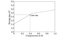
ObjectiveResonant cavity light emitting diode (RCLED) has wide applications in fields such as display lighting and optical fiber communication due to its superior features and lower cost compared with ordinary light emitting diodes (LEDs) and vertical-cavity surface-emitting laser (VCSEL). RCLED with an outgoing wavelength of 650 nm needs to be coupled with optical fiber for plastic fiber communication, the coupling efficiency is related to the far-field distribution of outgoing light of RCLED. In addition, the temperature change will affect the far-field distribution of outgoing light of RCLED. As an important component of RCLED, distributed Bragg reflectors (DBRs) have an important influence on the performance of RCLED devices. Therefore, it is of great significance to study the influence of temperature on DBR characteristics. In this paper, the DBR structure is designed and prepared based on RCLED of 650 nm. The effect of temperature change on the reflection spectrum of DBR is simulated, and the white light reflection spectrum of DBR is tested by the test equipment to verify the correctness of the simulation results.MethodsIn order to study the effect of temperature on DBR characteristics, the conclusion is drawn through theoretical simulation, and the experiments are used to verify the conclusion. First of all, the DBR structure based on RCLED of 650 nm is designed, and the material based on DBR must have the characteristic of a high and low refractive index material. In terms of material selection, by considering the absorption of red light and the oxidation of materials, the high and low refractive index materials are selected as Al0.5Ga0.5As and Al0.95Ga0.05As respectively. After determining the constituent material of the DBR, through the fitting function of the refractive index of AlxGa1-xAs material given in "the refractive index of AlxGa1-xAs below the band gap: accurate determination and empirical modeling", the relationship between the refractive index of AlxGa1-xAs and the incident wavelength, temperature, and the component of Al is obtained. Then we further determine the refractive index of Al0.5Ga0.5As and Al0.95Ga0.05As at room temperature at 650 nm and select the constituent log of DBR as 30 pairs. Later, the reflection spectrum of the DBR composed of 30 pairs of Al0.5Ga0.5As and Al0.95Ga0.05As at different temperatures is simulated, and the temperature characteristics of the theoretically simulated DBR are obtained. Finally, the designed DBR structure is prepared by the metal-organic chemical vapor deposition (MOCVD) experiment and tested, and the temperature characteristics of the experimental DBR are obtained and compared with the theoretically simulated results.Results and DiscussionsFirstly, for the RCLED of 650 nm-based DBR design, in terms of the selection of materials constituting DBR, based on the relationship between the band width of AlxGa1-xAs material and Al (Fig. 1), the material with higher refractive index is determined to be Al0.5Ga0.5As, and as the component of Al gets higher, the device oxidation is more likely to happen. The material with a lower refractive index is determined as Al0.95Ga0.05As. Then, by the fitting function of the refractive index of AlxGa1-xAs and the three variables, namely the component of Al, temperature, and incident wavelength (Eq. 3), the relationship between the refractive index of AlxGa1-xAs and these three variables is obtained (Fig. 2) at 293.15 K with the incident wavelength of 650 nm. The refractive indices of Al0.5Ga0.5As and Al0.95Ga0.05As are 3.4386 and 3.1215, respectively; the thickness of Al0.5Ga0.5As and Al0.95Ga0.05As is determined as 47.258 nm and 52.059 nm, respectively in room temperature. Later, the pairs of DBR are determined as 30 by the relationship between the reflectivity and pairs of the DBR in different material combinations (Fig. 3). Then, according to the theory of thin film transmission matrix, the reflection spectrum of the DBR at different temperatures is simulated (Fig. 4), and it is found that the reflection spectrum of DBR moves towards the long wavelength and then through the central reflection wavelength of DBR at different temperatures (Fig. 5). The temperature drift rate of the central reflection wavelength of DBR is 0.048982 nm/℃. Finally, the designed DBR is prepared through the MOCVD experiment, and the white light reflection spectra at different temperatures are tested (Fig. 6). The redshift of DBR with the temperature is obtained. According to the relationship between the central reflection wavelength of DBR and temperature (Fig. 7), the drift rate of the center wavelength with temperature is 0.049277 nm /℃.ConclusionsFor the far-field distribution of RCLED, the DBR structure based on RCLED of 650 nm is designed, and then the effect of temperature on DBR characteristics is analyzed. Temperature changes the optical thickness of each layer of the DBR by affecting the refractive index of the material AlxGa1-xAs of the DBR, thus affecting the reflection spectrum of the DBR. According to the theoretically simulated results, the reflection spectrum of DBR appears redshifted to the long wavelength as the temperature increases, and the temperature drift rate of the reflected wavelength of the DBR is calculated by linear fitting. From the experimental test results, as the temperature increases, the white light reflection spectrum of the prepared DBR also appears redshift phenomenon, and the temperature drift rate of the DBR central reflection wavelength calculated by linear fitting is not much different from the theoretically simulated results, which verifies the theoretical simulation. The analysis of the temperature characteristics of DBR makes the device designed at high temperature realize the wavelength matching between quantum trap and DBR, the conclusion has certain guiding significance for designing VCSEL devices with higher temperature sensitivity. ObjectiveResonant cavity light emitting diode (RCLED) has wide applications in fields such as display lighting and optical fiber communication due to its superior features and lower cost compared with ordinary light emitting diodes (LEDs) and vertical-cavity surface-emitting laser (VCSEL). RCLED with an outgoing wavelength of 650 nm needs to be coupled with optical fiber for plastic fiber communication, the coupling efficiency is related to the far-field distribution of outgoing light of RCLED. In addition, the temperature change will affect the far-field distribution of outgoing light of RCLED. As an important component of RCLED, distributed Bragg reflectors (DBRs) have an important influence on the performance of RCLED devices. Therefore, it is of great significance to study the influence of temperature on DBR characteristics. In this paper, the DBR structure is designed and prepared based on RCLED of 650 nm. The effect of temperature change on the reflection spectrum of DBR is simulated, and the white light reflection spectrum of DBR is tested by the test equipment to verify the correctness of the simulation results.MethodsIn order to study the effect of temperature on DBR characteristics, the conclusion is drawn through theoretical simulation, and the experiments are used to verify the conclusion. First of all, the DBR structure based on RCLED of 650 nm is designed, and the material based on DBR must have the characteristic of a high and low refractive index material. In terms of material selection, by considering the absorption of red light and the oxidation of materials, the high and low refractive index materials are selected as Al0.5Ga0.5As and Al0.95Ga0.05As respectively. After determining the constituent material of the DBR, through the fitting function of the refractive index of AlxGa1-xAs material given in "the refractive index of AlxGa1-xAs below the band gap: accurate determination and empirical modeling", the relationship between the refractive index of AlxGa1-xAs and the incident wavelength, temperature, and the component of Al is obtained. Then we further determine the refractive index of Al0.5Ga0.5As and Al0.95Ga0.05As at room temperature at 650 nm and select the constituent log of DBR as 30 pairs. Later, the reflection spectrum of the DBR composed of 30 pairs of Al0.5Ga0.5As and Al0.95Ga0.05As at different temperatures is simulated, and the temperature characteristics of the theoretically simulated DBR are obtained. Finally, the designed DBR structure is prepared by the metal-organic chemical vapor deposition (MOCVD) experiment and tested, and the temperature characteristics of the experimental DBR are obtained and compared with the theoretically simulated results.Results and DiscussionsFirstly, for the RCLED of 650 nm-based DBR design, in terms of the selection of materials constituting DBR, based on the relationship between the band width of AlxGa1-xAs material and Al (Fig. 1), the material with higher refractive index is determined to be Al0.5Ga0.5As, and as the component of Al gets higher, the device oxidation is more likely to happen. The material with a lower refractive index is determined as Al0.95Ga0.05As. Then, by the fitting function of the refractive index of AlxGa1-xAs and the three variables, namely the component of Al, temperature, and incident wavelength (Eq. 3), the relationship between the refractive index of AlxGa1-xAs and these three variables is obtained (Fig. 2) at 293.15 K with the incident wavelength of 650 nm. The refractive indices of Al0.5Ga0.5As and Al0.95Ga0.05As are 3.4386 and 3.1215, respectively; the thickness of Al0.5Ga0.5As and Al0.95Ga0.05As is determined as 47.258 nm and 52.059 nm, respectively in room temperature. Later, the pairs of DBR are determined as 30 by the relationship between the reflectivity and pairs of the DBR in different material combinations (Fig. 3). Then, according to the theory of thin film transmission matrix, the reflection spectrum of the DBR at different temperatures is simulated (Fig. 4), and it is found that the reflection spectrum of DBR moves towards the long wavelength and then through the central reflection wavelength of DBR at different temperatures (Fig. 5). The temperature drift rate of the central reflection wavelength of DBR is 0.048982 nm/℃. Finally, the designed DBR is prepared through the MOCVD experiment, and the white light reflection spectra at different temperatures are tested (Fig. 6). The redshift of DBR with the temperature is obtained. According to the relationship between the central reflection wavelength of DBR and temperature (Fig. 7), the drift rate of the center wavelength with temperature is 0.049277 nm /℃.ConclusionsFor the far-field distribution of RCLED, the DBR structure based on RCLED of 650 nm is designed, and then the effect of temperature on DBR characteristics is analyzed. Temperature changes the optical thickness of each layer of the DBR by affecting the refractive index of the material AlxGa1-xAs of the DBR, thus affecting the reflection spectrum of the DBR. According to the theoretically simulated results, the reflection spectrum of DBR appears redshifted to the long wavelength as the temperature increases, and the temperature drift rate of the reflected wavelength of the DBR is calculated by linear fitting. From the experimental test results, as the temperature increases, the white light reflection spectrum of the prepared DBR also appears redshift phenomenon, and the temperature drift rate of the DBR central reflection wavelength calculated by linear fitting is not much different from the theoretically simulated results, which verifies the theoretical simulation. The analysis of the temperature characteristics of DBR makes the device designed at high temperature realize the wavelength matching between quantum trap and DBR, the conclusion has certain guiding significance for designing VCSEL devices with higher temperature sensitivity.
Acta Optica Sinica
- Publication Date: Jul. 25, 2023
- Vol. 43, Issue 14, 1425002 (2023)

Reconfigurable Nested Photonic Loops Based on Valley Topological Boundary Waveguides
Yuxiao Jiang, and Yuntuan Fang
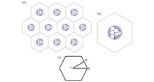
ObjectiveThe valley topological edge states (VTESs) and resonance loops are both important in optical communication systems, but they are usually two separate structures. In this paper, multi-layer nested valley photonic topological structures are designed. The energy transfer between loops is realized through the coupling of the evanescent field. By choosing its resonance frequency or changing the position of the light source, each loop has its own resonance frequency, and single loop or multiple-layer loops can be solely excited in the nested layered structure. Compared with similar studies, the loops do not design defects to form a resonant cavity and thus retain the integrity of the valley photonic crystal structures. This design has both the functionalities of resonance and waveguide transmission and increases the density of transmission channels. The results have application value in the reconfigurable photonic circuits.MethodsQuantum valley Hall effects (QVHEs) are realized by introducing angular rotation of the electron wave function at points K and K' in the first Brillouin zone (BZ), which provides an intrinsic magnetic moment, analogous to that provided by the electron spin. Similarly, vortex chirality (i.e., pseudospin) of photonic energy flow provides a new degree of freedom for optical waves via the orbital angular momentum, which can be realized by reducing the lattice rotation symmetry. By constructing different types of domain walls via these structures, valley edge states can be achieved. Firstly, it is necessary to construct a two-dimensional photonic crystal unit cell. The design of the unit cell structure in this article takes into account that Bragg-scattering not only exists between lattices but also occurs between the various medium columns within the lattice. In order to obtain a wider bandgap, the method of rotating the medium columns is used to break the spatial symmetry of the photonic crystal so that the degeneracy at the high-symmetry point K in the first BZ of the reciprocal lattice is separated, thereby showing a complete bandgap in the energy band diagram. Subsequently, by analyzing the phase difference between the two lattices at point K after rotating the medium columns (i.e., the topological invariant), it is proved that the structure has opposite topological phases at the K point, thereby indicating that the edge mode is the topological boundary mode. Secondly, by periodically arranging the two lattices, a supercell can be formed. After the frequency domain simulation, the supercell in this article has two edge states, and the spin-locked properties of the VTESs can be studied. Based on the above studies, we construct a nested loop model to achieve energy exchange between photonic crystals in the form of loop coupling. The principle of this coupling is evanescent field coupling. Compared with most current coupling methods that use waveguides and cavities, evanescent field coupling does not require the construction of waveguides or other defects or cavities. The topological edge mode of the valley photonic crystal designed in this article has great local properties and does not require additional defects. Last but not least, based on the advantages of topological properties, the design can also achieve efficient transmission while maintaining the original structure.Results and DiscussionsWe propose a new reconfigurable topological photonic structure model, which is a multi-layer nested photonic topological ring similar to Russian dolls. Based on the one-way transmission property of topological boundary states and the theory of coupling of electromagnetic waves, a three-layer nested loop (Fig. 7) is designed. The source position is at the center of any loop, and when the frequency is the same, different source positions will excite different transmission channels of the circuit. Furthermore, keeping the source position unchanged and changing the frequency of the source can excite multiple transmission channels. According to statistics (Fig. 8 and Fig. 9), the transmission channels in the structure will exhibit diverse forms such as single external loop, single inner loop, single middle loop, as well as double loops and triple loops. Compared with other similar schemes, the model design in this paper is intuitive, and there are no transmission channels connecting the loops. Energy transmission is entirely carried out by the coupling of the evanescent field to achieve reconfigurability. Its reconfigurability does not require any external conditions, which greatly reduces the complexity and difficulty of the design.ConclusionsThe VTES has become a new research hotspot in topological photonics because of its flexibility and diversity. In this paper, reconfigurable topological channels in the form of multiple-layer nested loops have been designed. By combining the topological edge states of the valley photonic crystal with the resonance loops, a variety of different channels can be excited. Although the reconfigurable topological waveguides have been widely studied, the unique value of our design is that the reconfigurable method does not rely on external conditions; instead, single or multilayer circuits can be selectively excited by setting the location and frequency of the source. This model can be used as a multi-channel frequency selector or optical resonator. Different from the general selector and resonator, the channel in the structure is a topological loop, which combines the common characteristics of topological protection and resonance, so as to reduce the loss as far as possible. It provides a new idea for the application of VTESs in optical devices. ObjectiveThe valley topological edge states (VTESs) and resonance loops are both important in optical communication systems, but they are usually two separate structures. In this paper, multi-layer nested valley photonic topological structures are designed. The energy transfer between loops is realized through the coupling of the evanescent field. By choosing its resonance frequency or changing the position of the light source, each loop has its own resonance frequency, and single loop or multiple-layer loops can be solely excited in the nested layered structure. Compared with similar studies, the loops do not design defects to form a resonant cavity and thus retain the integrity of the valley photonic crystal structures. This design has both the functionalities of resonance and waveguide transmission and increases the density of transmission channels. The results have application value in the reconfigurable photonic circuits.MethodsQuantum valley Hall effects (QVHEs) are realized by introducing angular rotation of the electron wave function at points K and K' in the first Brillouin zone (BZ), which provides an intrinsic magnetic moment, analogous to that provided by the electron spin. Similarly, vortex chirality (i.e., pseudospin) of photonic energy flow provides a new degree of freedom for optical waves via the orbital angular momentum, which can be realized by reducing the lattice rotation symmetry. By constructing different types of domain walls via these structures, valley edge states can be achieved. Firstly, it is necessary to construct a two-dimensional photonic crystal unit cell. The design of the unit cell structure in this article takes into account that Bragg-scattering not only exists between lattices but also occurs between the various medium columns within the lattice. In order to obtain a wider bandgap, the method of rotating the medium columns is used to break the spatial symmetry of the photonic crystal so that the degeneracy at the high-symmetry point K in the first BZ of the reciprocal lattice is separated, thereby showing a complete bandgap in the energy band diagram. Subsequently, by analyzing the phase difference between the two lattices at point K after rotating the medium columns (i.e., the topological invariant), it is proved that the structure has opposite topological phases at the K point, thereby indicating that the edge mode is the topological boundary mode. Secondly, by periodically arranging the two lattices, a supercell can be formed. After the frequency domain simulation, the supercell in this article has two edge states, and the spin-locked properties of the VTESs can be studied. Based on the above studies, we construct a nested loop model to achieve energy exchange between photonic crystals in the form of loop coupling. The principle of this coupling is evanescent field coupling. Compared with most current coupling methods that use waveguides and cavities, evanescent field coupling does not require the construction of waveguides or other defects or cavities. The topological edge mode of the valley photonic crystal designed in this article has great local properties and does not require additional defects. Last but not least, based on the advantages of topological properties, the design can also achieve efficient transmission while maintaining the original structure.Results and DiscussionsWe propose a new reconfigurable topological photonic structure model, which is a multi-layer nested photonic topological ring similar to Russian dolls. Based on the one-way transmission property of topological boundary states and the theory of coupling of electromagnetic waves, a three-layer nested loop (Fig. 7) is designed. The source position is at the center of any loop, and when the frequency is the same, different source positions will excite different transmission channels of the circuit. Furthermore, keeping the source position unchanged and changing the frequency of the source can excite multiple transmission channels. According to statistics (Fig. 8 and Fig. 9), the transmission channels in the structure will exhibit diverse forms such as single external loop, single inner loop, single middle loop, as well as double loops and triple loops. Compared with other similar schemes, the model design in this paper is intuitive, and there are no transmission channels connecting the loops. Energy transmission is entirely carried out by the coupling of the evanescent field to achieve reconfigurability. Its reconfigurability does not require any external conditions, which greatly reduces the complexity and difficulty of the design.ConclusionsThe VTES has become a new research hotspot in topological photonics because of its flexibility and diversity. In this paper, reconfigurable topological channels in the form of multiple-layer nested loops have been designed. By combining the topological edge states of the valley photonic crystal with the resonance loops, a variety of different channels can be excited. Although the reconfigurable topological waveguides have been widely studied, the unique value of our design is that the reconfigurable method does not rely on external conditions; instead, single or multilayer circuits can be selectively excited by setting the location and frequency of the source. This model can be used as a multi-channel frequency selector or optical resonator. Different from the general selector and resonator, the channel in the structure is a topological loop, which combines the common characteristics of topological protection and resonance, so as to reduce the loss as far as possible. It provides a new idea for the application of VTESs in optical devices.
Acta Optica Sinica
- Publication Date: Jul. 25, 2023
- Vol. 43, Issue 14, 1425001 (2023)
Detection Probability Model and Verification of an Improved Single-Photon Avalanche Diode
Zhixiang Cao, Meiling Zeng, Jian Yang, and Xiangliang Jin
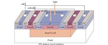
ObjectiveA method considering the light transmission of silicon dioxide film on the device surface can be proposed to address the large error between the existing photon detection probability (PDP) model and actual test results, which can accurately predict the detection probability of single-photon avalanche diodes (SPADs). Visible light communication requires a high-sensitivity receiver to receive optical signals, and single-photon detectors play an extremely important role in visible light communication because of their high sensitivity, high gain, and high visible light wide-spectrum response. Due to the time-consuming and cost-intensive bipolar-complementary metal oxide semiconductor-double diffusion metal oxide semiconductor (BCD) process workflow, prediction of SPAD performance is critical to optimize its design before fabrication. Although commercial semiconductor simulation software can usually simulate the electrical properties of SPADs, such as breakdown voltage, impact ionization rate, and electric field distribution, their statistical performance cannot be directly simulated. Additionally, since the internal operating mechanism of the semiconductor simulation software is not open, it is impossible to know the detailed simulation process, and it is also prone to non-convergence during the simulation. Therefore, it is of practical significance to model the performance parameters of SPADs. In fact, although there are some theoretical models for the calculation of PDP, due to the complex factors of its physical process, various models have large errors and are inconsistent with the experimental test trend in the short wavelength range. Thus, the photon-quantitative and reliable prediction of detection probability is challenging.MethodsThe PDP is defined as the product of the light transmission of a photon passing through the silicon dioxide layer on the silicon surface and the internal quantum efficiency of the device. The internal quantum efficiency of the device is the probability triggered when a photon is absorbed by the device and results in an avalanche. The internal quantum efficiency of P+/N well/deep N well SPAD is divided into three parts. In the neutral region P, photons are absorbed in the P+ layer on top of the SPAD to generate electron-hole pairs, and some photogenerated electrons will diffuse to the upper boundary of the depletion region, triggering an avalanche probability. In the depletion region, photogenerated electrons and holes drift in opposite directions under the action of a strong electric field in this region and trigger an avalanche after moving a very short distance. In the neutral region N, photogenerated holes can reach the bottom of the depletion region without being recombined, and initiate an avalanche trigger. In this study, the doping concentration provided by the device processing factory and the designed SPAD layout structure are imported into the TCAD tool to rebuild the two-dimensional device model. Through the function library that comes with Sentaurus Sdevice, parameters such as temperature, bias voltage, and incident light wavelength are set for electrical simulation, and the electric field intensity and width of the depletion region are obtained. Then, the electric field strength and the width of the depletion region are imported into the model built by Matlab software to obtain the internal quantum efficiency. The particle swarm optimization algorithm is adopted to obtain the fitting parameters of the transmission spectrum in the passivation layer of the silicon dioxide film, and finally acquire the PDP.Results and DiscussionsFirstly, two-dimensional process simulations are carried out through the Sentaurus SED based on the standard 0.18 μm BCD process and the SPAD device structure obtained from the process simulations. The simulated electric field distribution of the SPAD at an excess bias voltage of 1 V is simulated by Sentaurus Sdevice (Fig. 4) to extract the one-dimensional (1D) electric field distribution at the center of the device at an excess bias voltage of 1 V (Fig. 5). The electric field distributions at 0.5, 1.0, 2.0, and 3.0 V over-bias respectively are employed to calculate the avalanche trigger probability at each location in the depletion region (Fig. 6). The theoretical model of the PDP is improved by considering the effect of the silica passivation layer film on the incident light wavelength. The wavelength-dependent transmission of the silica film is fitted through a particle swarm optimization algorithm by comparing the theoretical model with experimental test results (Fig. 7). The PDPs contributed by each of the three components of the neutral P, depletion, and neutral N regions are calculated (Fig. 8), and the total PDP is the sum of the three components (Fig. 9). Finally, a PDP model with a low mean error is achieved (Fig. 10). The results show good agreement between the PDP predictions and experimental tests, with an average error of only 1.72%.ConclusionsWe discuss the PDP for simulating typical over-bias voltages from 0.5 to 3 V without substrate contribution. The model and experimental test results are compared at the over-bias voltage of 0.5 V with an average error of only 1.72%. The average error is defined as the average of the sum of the absolute errors for each wavelength. The improved model for PDP considering the transmission spectrum of a thin film of silica passivation layer provides a research direction for the development of new SPAD device structures. Results show that the model can reduce the non-convergence problems in commercial device simulation software, and greatly reduce the time and cost required to develop new structures for SPAD devices. Additionally, the building of models for electric field strength, avalanche trigger probability, and carrier lifetime can help dark counting analysis, thus enlightening related researchers. ObjectiveA method considering the light transmission of silicon dioxide film on the device surface can be proposed to address the large error between the existing photon detection probability (PDP) model and actual test results, which can accurately predict the detection probability of single-photon avalanche diodes (SPADs). Visible light communication requires a high-sensitivity receiver to receive optical signals, and single-photon detectors play an extremely important role in visible light communication because of their high sensitivity, high gain, and high visible light wide-spectrum response. Due to the time-consuming and cost-intensive bipolar-complementary metal oxide semiconductor-double diffusion metal oxide semiconductor (BCD) process workflow, prediction of SPAD performance is critical to optimize its design before fabrication. Although commercial semiconductor simulation software can usually simulate the electrical properties of SPADs, such as breakdown voltage, impact ionization rate, and electric field distribution, their statistical performance cannot be directly simulated. Additionally, since the internal operating mechanism of the semiconductor simulation software is not open, it is impossible to know the detailed simulation process, and it is also prone to non-convergence during the simulation. Therefore, it is of practical significance to model the performance parameters of SPADs. In fact, although there are some theoretical models for the calculation of PDP, due to the complex factors of its physical process, various models have large errors and are inconsistent with the experimental test trend in the short wavelength range. Thus, the photon-quantitative and reliable prediction of detection probability is challenging.MethodsThe PDP is defined as the product of the light transmission of a photon passing through the silicon dioxide layer on the silicon surface and the internal quantum efficiency of the device. The internal quantum efficiency of the device is the probability triggered when a photon is absorbed by the device and results in an avalanche. The internal quantum efficiency of P+/N well/deep N well SPAD is divided into three parts. In the neutral region P, photons are absorbed in the P+ layer on top of the SPAD to generate electron-hole pairs, and some photogenerated electrons will diffuse to the upper boundary of the depletion region, triggering an avalanche probability. In the depletion region, photogenerated electrons and holes drift in opposite directions under the action of a strong electric field in this region and trigger an avalanche after moving a very short distance. In the neutral region N, photogenerated holes can reach the bottom of the depletion region without being recombined, and initiate an avalanche trigger. In this study, the doping concentration provided by the device processing factory and the designed SPAD layout structure are imported into the TCAD tool to rebuild the two-dimensional device model. Through the function library that comes with Sentaurus Sdevice, parameters such as temperature, bias voltage, and incident light wavelength are set for electrical simulation, and the electric field intensity and width of the depletion region are obtained. Then, the electric field strength and the width of the depletion region are imported into the model built by Matlab software to obtain the internal quantum efficiency. The particle swarm optimization algorithm is adopted to obtain the fitting parameters of the transmission spectrum in the passivation layer of the silicon dioxide film, and finally acquire the PDP.Results and DiscussionsFirstly, two-dimensional process simulations are carried out through the Sentaurus SED based on the standard 0.18 μm BCD process and the SPAD device structure obtained from the process simulations. The simulated electric field distribution of the SPAD at an excess bias voltage of 1 V is simulated by Sentaurus Sdevice (Fig. 4) to extract the one-dimensional (1D) electric field distribution at the center of the device at an excess bias voltage of 1 V (Fig. 5). The electric field distributions at 0.5, 1.0, 2.0, and 3.0 V over-bias respectively are employed to calculate the avalanche trigger probability at each location in the depletion region (Fig. 6). The theoretical model of the PDP is improved by considering the effect of the silica passivation layer film on the incident light wavelength. The wavelength-dependent transmission of the silica film is fitted through a particle swarm optimization algorithm by comparing the theoretical model with experimental test results (Fig. 7). The PDPs contributed by each of the three components of the neutral P, depletion, and neutral N regions are calculated (Fig. 8), and the total PDP is the sum of the three components (Fig. 9). Finally, a PDP model with a low mean error is achieved (Fig. 10). The results show good agreement between the PDP predictions and experimental tests, with an average error of only 1.72%.ConclusionsWe discuss the PDP for simulating typical over-bias voltages from 0.5 to 3 V without substrate contribution. The model and experimental test results are compared at the over-bias voltage of 0.5 V with an average error of only 1.72%. The average error is defined as the average of the sum of the absolute errors for each wavelength. The improved model for PDP considering the transmission spectrum of a thin film of silica passivation layer provides a research direction for the development of new SPAD device structures. Results show that the model can reduce the non-convergence problems in commercial device simulation software, and greatly reduce the time and cost required to develop new structures for SPAD devices. Additionally, the building of models for electric field strength, avalanche trigger probability, and carrier lifetime can help dark counting analysis, thus enlightening related researchers.
Acta Optica Sinica
- Publication Date: May. 25, 2023
- Vol. 43, Issue 10, 1025002 (2023)
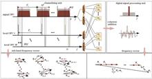
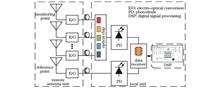
Photonics-Assisted Sensing of Non-Repetitive Transient Weak Signal with Sensitivity Enhancement
Bing Lu, Fangge Fu, Xiaoxia Zhang, Xianglei Yan, and Xiaojin Guo
ObjectiveThe non-repetitive transient weak signal exists in diverse fields, such as astronomy, spectroscopy, and biology, and it is difficult to be perceived and analyzed due to its short duration, large instantaneous bandwidth, unexpected arrival time, and low power. Over the past years, photonic technology has witnessed remarkable progress in the wideband and weak signal loss in the noise. For example, the signal stands out from the noise by using the Talbot effect to redistribute the energy of repetitive waveforms into fewer replicas for noiseless intensity amplification and avoiding digital post-processing. However, it is only valid for repetitive waveforms. A spectral cloning receiver based on coherent dual optical frequency combs (OFCs) is proposed to detect a random non-repetitive signal hidden in the noise. In this proposal, the spectrum of the received signal is sliced into a series of sub-bands (or channels) due to the difference in the free spectrum ranges (FSRs) of two combs. Then, coherent in-phase summation of these sub-bands can lead to a signal-to-noise ratio (SNR) increase (10lg S) linearly proportional to the cloning count or the available sub-bands, which is associated with the effective comb line of the coherent dual OFCs (S). In order to achieve a large SNR improvement, considerable comb lines of the OFCs must be required. However, generating massive comb lines not only needs high input radio frequencies (RFs) and laser powers but also needs superior optoelectronic hardware, which makes the system complex and costly. In addition, the comb channel number is also constrained by the available wavelength range. Therefore, a novel method using a single comb-based scheme for deep denoising in covert wireless communication is proposed. However, it also faces the problem that the system is difficult to further increase the number of comb lines. At this time, a method is urgently needed to effectively solve the problems of the above methods.MethodsTo this end, a novel photonic approach to enhance the sensing sensitivity of non-repetitive transient weak signals in a noisy background is proposed. Based on a coherent dual OFCs-assisted spectral cloning receiver, thetransient signal is firstly multicast by N-line signal OFCs and then split equally into M copies, while the local OFC is replicated to multiple replicas by multiple acousto-optic frequency shifters (AOFSs). Therefore, the spectrum of the received transient signal is decomposed into N×M sub-bands. Subsequently, different spectral slices are extracted and down-converted to the same intermediate frequency by an I/Q demodulator. Finally, all the sub-band signals are processed in digital signal processing (DSP) and positively superimposed in the frequency domain. Since the phase characteristics of the spectrum in each sub-channel are in-phase, but the noise frequency spectrum is random, the collinear superposition of the signal spectral vector will be realized, while the noise is randomly superimposed, which leads to a multiplied SNR enhancement of N × M for the transient signal sensing.Results and DiscussionsA spectral cloning receiving scheme based on the dual coherent OFCs with nine comb lines is used to perceive a transient signal. The performance of the system is characterized by an 18-GHz wide pulse at various noise levels. As the scatter diagram shows, the separation degree of signal cloud and noise cloud is greater than that of the single channel after 18 channels are superimposed in phase with one AOFS used (N=9 and M=2). Compared with that of a single channel, the detection sensitivity increases by 3 dB after spectral cloning, which is consistent with the theoretical value (Fig. 5). The local OFC and signal OFC are replicated 1, 2, and 3 times, and the detection gain is improved by 3.0 dB, 4.5 dB, and 5.9 dB, reaching to 12.63 dB, 14.04 dB, and 15.43 dB, respectively, which accord well with the theoretical value (Fig. 7). In this proposal, the complexity of the OFC generation module and the spectral coverage do not increase basically, but a multiplied SNR rise is achieved. In addition, the splitting loss induced by the optical couplers (OCs) will cause a faint power at the detectors so that the system cannot detect the optical signals. Although Erbium-doped fiber amplifiers (EDFAs) can compensate for the loss, the spontaneous emission noise introduced by EDFAs will greatly influence the detection gain of the system. Therefore, it is necessary to select the appropriate splitting number according to the actual link characteristics, such as EDFA's noise and detector sensitivity.ConclusionsA simplified and low-cost spectral cloning receiver using multiple AOFSs for large SNR enhancement is proposed and demonstrated. Based on the dual OFC channelization scheme, multiple AOFSs and OCs are used to replicate the local OFC and modulated signal so that the spectrum of the received transient signal is divided into multiple sub-bands. After the collinear superposition of the sub-band signal spectrum and the random superposition of the noise spectrum, the detection sensitivity of the transient weak signal is greatly improved. The dual-OFCs spectral cloning receiver with nine lines is used to detect the sub-noise transient signal with a bandwidth of 18 GHz. The detection sensitivity gain is increased to 12.63 dB, 14.04 dB, and 15.43 dB under varying noise power conditions by replicating the local OFC 1, 2, and 3 times. Compared with the previous scheme, the proposed scheme requires fewer optical frequency comb lines and a smaller available wavelength range to achieve the same SNR improvement under the available sensitivity of the receiving unit. ObjectiveThe non-repetitive transient weak signal exists in diverse fields, such as astronomy, spectroscopy, and biology, and it is difficult to be perceived and analyzed due to its short duration, large instantaneous bandwidth, unexpected arrival time, and low power. Over the past years, photonic technology has witnessed remarkable progress in the wideband and weak signal loss in the noise. For example, the signal stands out from the noise by using the Talbot effect to redistribute the energy of repetitive waveforms into fewer replicas for noiseless intensity amplification and avoiding digital post-processing. However, it is only valid for repetitive waveforms. A spectral cloning receiver based on coherent dual optical frequency combs (OFCs) is proposed to detect a random non-repetitive signal hidden in the noise. In this proposal, the spectrum of the received signal is sliced into a series of sub-bands (or channels) due to the difference in the free spectrum ranges (FSRs) of two combs. Then, coherent in-phase summation of these sub-bands can lead to a signal-to-noise ratio (SNR) increase (10lg S) linearly proportional to the cloning count or the available sub-bands, which is associated with the effective comb line of the coherent dual OFCs (S). In order to achieve a large SNR improvement, considerable comb lines of the OFCs must be required. However, generating massive comb lines not only needs high input radio frequencies (RFs) and laser powers but also needs superior optoelectronic hardware, which makes the system complex and costly. In addition, the comb channel number is also constrained by the available wavelength range. Therefore, a novel method using a single comb-based scheme for deep denoising in covert wireless communication is proposed. However, it also faces the problem that the system is difficult to further increase the number of comb lines. At this time, a method is urgently needed to effectively solve the problems of the above methods.MethodsTo this end, a novel photonic approach to enhance the sensing sensitivity of non-repetitive transient weak signals in a noisy background is proposed. Based on a coherent dual OFCs-assisted spectral cloning receiver, thetransient signal is firstly multicast by N-line signal OFCs and then split equally into M copies, while the local OFC is replicated to multiple replicas by multiple acousto-optic frequency shifters (AOFSs). Therefore, the spectrum of the received transient signal is decomposed into N×M sub-bands. Subsequently, different spectral slices are extracted and down-converted to the same intermediate frequency by an I/Q demodulator. Finally, all the sub-band signals are processed in digital signal processing (DSP) and positively superimposed in the frequency domain. Since the phase characteristics of the spectrum in each sub-channel are in-phase, but the noise frequency spectrum is random, the collinear superposition of the signal spectral vector will be realized, while the noise is randomly superimposed, which leads to a multiplied SNR enhancement of N × M for the transient signal sensing.Results and DiscussionsA spectral cloning receiving scheme based on the dual coherent OFCs with nine comb lines is used to perceive a transient signal. The performance of the system is characterized by an 18-GHz wide pulse at various noise levels. As the scatter diagram shows, the separation degree of signal cloud and noise cloud is greater than that of the single channel after 18 channels are superimposed in phase with one AOFS used (N=9 and M=2). Compared with that of a single channel, the detection sensitivity increases by 3 dB after spectral cloning, which is consistent with the theoretical value (Fig. 5). The local OFC and signal OFC are replicated 1, 2, and 3 times, and the detection gain is improved by 3.0 dB, 4.5 dB, and 5.9 dB, reaching to 12.63 dB, 14.04 dB, and 15.43 dB, respectively, which accord well with the theoretical value (Fig. 7). In this proposal, the complexity of the OFC generation module and the spectral coverage do not increase basically, but a multiplied SNR rise is achieved. In addition, the splitting loss induced by the optical couplers (OCs) will cause a faint power at the detectors so that the system cannot detect the optical signals. Although Erbium-doped fiber amplifiers (EDFAs) can compensate for the loss, the spontaneous emission noise introduced by EDFAs will greatly influence the detection gain of the system. Therefore, it is necessary to select the appropriate splitting number according to the actual link characteristics, such as EDFA's noise and detector sensitivity.ConclusionsA simplified and low-cost spectral cloning receiver using multiple AOFSs for large SNR enhancement is proposed and demonstrated. Based on the dual OFC channelization scheme, multiple AOFSs and OCs are used to replicate the local OFC and modulated signal so that the spectrum of the received transient signal is divided into multiple sub-bands. After the collinear superposition of the sub-band signal spectrum and the random superposition of the noise spectrum, the detection sensitivity of the transient weak signal is greatly improved. The dual-OFCs spectral cloning receiver with nine lines is used to detect the sub-noise transient signal with a bandwidth of 18 GHz. The detection sensitivity gain is increased to 12.63 dB, 14.04 dB, and 15.43 dB under varying noise power conditions by replicating the local OFC 1, 2, and 3 times. Compared with the previous scheme, the proposed scheme requires fewer optical frequency comb lines and a smaller available wavelength range to achieve the same SNR improvement under the available sensitivity of the receiving unit.
Acta Optica Sinica
- Publication Date: May. 25, 2023
- Vol. 43, Issue 10, 1025001 (2023)
Large-Scale Multi-Antenna and One-Receiver GNSS-over-Fiber Differential Positioning System Using Silicon On-Chip Optical Routing
Wu Xu, Xihua Zou, Peixuan Li, Linjie Zhou, Wei Pan, Lianshan Yan, Yang Li, Di Zheng, and Yongliang Peng
This paper proposes and experimentally validates a large-scale multi-antenna and one-receiver global navigation satellite system (GNSS)-over-fiber differential positioning system using silicon on-chip optical routing. The radio-over-fiber (RoF) distributed antenna architecture is utilized to facilitate remote multipoint GNSS signal acquisition, and RoF transmission links featuring low loss, large bandwidth, and immunity to electromagnetic interference are reaped to achieve the centralized reception of remotely collected GNSS signals at the local end. At this end, a complementary metal-oxide-semiconductor (CMOS)-process-compatible high-speed silicon optical switch chip is fabricated for the periodic switching and differential calculation of GNSS signals over fiber obtained at different monitoring points. Then, a time-division multiplexing-based multi-antenna and one-receiver GNSS positioning system using on-chip optical routing is built. In the experiments, a self-developed 1×8 thermo-optic silicon optical switch chip based on a Mach-Zehnder interferometer is employed to build an experimental multi-antenna GNSS positioning system with five remote monitoring points. The RoF transmission distance of the GNSS signals is 10 km. According to the experimental results, the real-time response time of the optical switch chip module is less than 200 μs. Stable and high-accuracy positioning at five remote monitoring points (10 km away) is achieved without the aid of additional optical amplification. The obtained positioning accuracy in the east (E), north (N), and up (U) directions is all at the millimeter level. This paper proposes and experimentally validates a large-scale multi-antenna and one-receiver global navigation satellite system (GNSS)-over-fiber differential positioning system using silicon on-chip optical routing. The radio-over-fiber (RoF) distributed antenna architecture is utilized to facilitate remote multipoint GNSS signal acquisition, and RoF transmission links featuring low loss, large bandwidth, and immunity to electromagnetic interference are reaped to achieve the centralized reception of remotely collected GNSS signals at the local end. At this end, a complementary metal-oxide-semiconductor (CMOS)-process-compatible high-speed silicon optical switch chip is fabricated for the periodic switching and differential calculation of GNSS signals over fiber obtained at different monitoring points. Then, a time-division multiplexing-based multi-antenna and one-receiver GNSS positioning system using on-chip optical routing is built. In the experiments, a self-developed 1×8 thermo-optic silicon optical switch chip based on a Mach-Zehnder interferometer is employed to build an experimental multi-antenna GNSS positioning system with five remote monitoring points. The RoF transmission distance of the GNSS signals is 10 km. According to the experimental results, the real-time response time of the optical switch chip module is less than 200 μs. Stable and high-accuracy positioning at five remote monitoring points (10 km away) is achieved without the aid of additional optical amplification. The obtained positioning accuracy in the east (E), north (N), and up (U) directions is all at the millimeter level.
Acta Optica Sinica
- Publication Date: Jan. 01, 2022
- Vol. 42, Issue 24, 2425001 (2022)

Quintuple Frequency-Tunable and Phase-Tunable Optoelectronic Oscillator Based on Stimulated Brillouin Scattering
Yue Wang, Wei Dong, and Shiyin Li
Optoelectronic oscillator (OEO), a microwave signal source, is a popular research topic in microwave photonics. A quintuple OEO with tunable frequency and phase is proposed and theoretically analyzed, which is based on the stimulated Brillouin scattering (SBS) effect and carrier phase-shifted single-sideband modulation. In this structure, a cascade modulator structure is used to generate five lights with the same power and frequency interval as the pump lights, and then the quintuple OEO is obtained by the Brillouin gain-loss compensation principle. The frequency-tunable microwave signal is obtained by using the Brillouin wavelength-dependent property, and phase-tunable output microwave signal is obtained by adjusting the dual-parallel Mach-Zehnder modulator. The designed OEO can output high-frequency microwave signals with a frequency tuning range of 44.00-47.25 GHz, and on this basis, it can achieve a tunable phase range of 0°-360°. Optoelectronic oscillator (OEO), a microwave signal source, is a popular research topic in microwave photonics. A quintuple OEO with tunable frequency and phase is proposed and theoretically analyzed, which is based on the stimulated Brillouin scattering (SBS) effect and carrier phase-shifted single-sideband modulation. In this structure, a cascade modulator structure is used to generate five lights with the same power and frequency interval as the pump lights, and then the quintuple OEO is obtained by the Brillouin gain-loss compensation principle. The frequency-tunable microwave signal is obtained by using the Brillouin wavelength-dependent property, and phase-tunable output microwave signal is obtained by adjusting the dual-parallel Mach-Zehnder modulator. The designed OEO can output high-frequency microwave signals with a frequency tuning range of 44.00-47.25 GHz, and on this basis, it can achieve a tunable phase range of 0°-360°.
Acta Optica Sinica
- Publication Date: Nov. 25, 2022
- Vol. 42, Issue 22, 2225001 (2022)
Effect of Electrostatic Field Inversion in (10
Ruimei Yin, Wei Jia, Hailiang Dong, Zhigang Jia, Tianbao Li, Chunyan Yu, Zhuxia Zhang, and Bingshe Xu
In this paper, polarization intensity as a function of crystallographic orientation is studied by the InGaN/GaN single quantum well model. The results reveal that the polarization electric field inversion in the semi-polar (101¯1) quantum well leads to upward bending of the energy band, and the electron wave function in the quantum well is close to the n-side, which is likely to successfully suppress electron leakage. The simulation of the epitaxial structure of (101¯1)-plane InGaN/GaN multi-quantum-well blue light-emitting diodes (LEDs) demonstrates that LEDs grown on the semi-polar (101¯1) plane can elevate the effective blocking barrier of the quantum barrier and suppress electron leakage. Moreover, the (101¯1) plane greatly reduces the hole injection barrier, promotes the even distribution of carriers, and reduces Auger recombination probability. Finally, the efficiency droop in (101¯1)-plane GaN-based LEDs is drastically reduced to 9% at the current density of 300 A/cm2 compared with 42% efficiency droop in the (0001) plane, and electroluminescence intensity is increased by 48%. The electrostatic field inversion of the (101¯1)-plane InGaN quantum well is an important reason for its excellent photoelectric properties. In this paper, polarization intensity as a function of crystallographic orientation is studied by the InGaN/GaN single quantum well model. The results reveal that the polarization electric field inversion in the semi-polar (101¯1) quantum well leads to upward bending of the energy band, and the electron wave function in the quantum well is close to the n-side, which is likely to successfully suppress electron leakage. The simulation of the epitaxial structure of (101¯1)-plane InGaN/GaN multi-quantum-well blue light-emitting diodes (LEDs) demonstrates that LEDs grown on the semi-polar (101¯1) plane can elevate the effective blocking barrier of the quantum barrier and suppress electron leakage. Moreover, the (101¯1) plane greatly reduces the hole injection barrier, promotes the even distribution of carriers, and reduces Auger recombination probability. Finally, the efficiency droop in (101¯1)-plane GaN-based LEDs is drastically reduced to 9% at the current density of 300 A/cm2 compared with 42% efficiency droop in the (0001) plane, and electroluminescence intensity is increased by 48%. The electrostatic field inversion of the (101¯1)-plane InGaN quantum well is an important reason for its excellent photoelectric properties.
Acta Optica Sinica
- Publication Date: Nov. 10, 2022
- Vol. 42, Issue 21, 2125001 (2022)
Ultra-Wideband Arrayed Microwave Photonic Processing Technology
Tao Zhou, Jingxian Liu, Zhiyu Chen, Ziang He, Aiping Xie, Xin Zhong, Yan Cui, and Minhui Long
Ultra-wideband arrays have been a trend of development of radar, communication, and electronic information systems. Microwave photonics (MWP), combining the advantages of both microwave and photonic technologies, will pave the way for the development of electronic information systems with novel mechanism. In this paper, the domestic and foreign research progresses of MWP are reviewed. A signal processing architecture based on MWP technologies and adapted to multiple scenarios is discussed. The research progresses in theories, experiments, and applications of typical MWP technologies, such as high quality signal generation, large dynamic signal transmission, phase stabilization of distributed signals, optical beamforming, and optical channelization, are described. In the end, the development trends of microwave photonics are expected. Ultra-wideband arrays have been a trend of development of radar, communication, and electronic information systems. Microwave photonics (MWP), combining the advantages of both microwave and photonic technologies, will pave the way for the development of electronic information systems with novel mechanism. In this paper, the domestic and foreign research progresses of MWP are reviewed. A signal processing architecture based on MWP technologies and adapted to multiple scenarios is discussed. The research progresses in theories, experiments, and applications of typical MWP technologies, such as high quality signal generation, large dynamic signal transmission, phase stabilization of distributed signals, optical beamforming, and optical channelization, are described. In the end, the development trends of microwave photonics are expected.
Acta Optica Sinica
- Publication Date: Sep. 10, 2022
- Vol. 42, Issue 17, 1725001 (2022)
Simulation Model of GaN-Based Micro-LED with High Light Extraction Efficiency
Xinpei Hu, Junhu Cai, Yuanyuan Ye, Enguo Chen, Jie Sun, Qun Yan, and Tailiang Guo
The reduction in the display chip size of micro light emitting diode (Micro-LED) exerts a sidewall effect and consequently results in a decreased forward light extraction efficiency (LEE). The display chip structure of Micro-LED with high LEE still needs to be further studied. For this reason, an optimized model of GaN-based Micro-LED with high LEE is explored by leveraging the finite-difference time-domain method from a simulation perspective. Specifically, the initial laminated structure of GaN-based Micro-LED with vertical sidewalls is constructed, and the influence of the sidewall effect on LEE is analyzed quantitatively. Then, the impact of the position change of multiple-quantum-well active layer in Micro-LED on the light output effect is investigated, and Micro-LED structure models with different inclined sidewall angles are analyzed. The influence of the bottom reflective material on LEE is discussed, and the parameters of the preliminarily optimized GaN-based Micro-LED model are obtained. Finally, LEE is further improved by designing a top transmission grating, and the effects of period, height, and duty cycle on LEE are examined. The results show that the overall LEE of the optimized GaN-based Micro-LED is 2.42 times higher than that of the initial structure. The reduction in the display chip size of micro light emitting diode (Micro-LED) exerts a sidewall effect and consequently results in a decreased forward light extraction efficiency (LEE). The display chip structure of Micro-LED with high LEE still needs to be further studied. For this reason, an optimized model of GaN-based Micro-LED with high LEE is explored by leveraging the finite-difference time-domain method from a simulation perspective. Specifically, the initial laminated structure of GaN-based Micro-LED with vertical sidewalls is constructed, and the influence of the sidewall effect on LEE is analyzed quantitatively. Then, the impact of the position change of multiple-quantum-well active layer in Micro-LED on the light output effect is investigated, and Micro-LED structure models with different inclined sidewall angles are analyzed. The influence of the bottom reflective material on LEE is discussed, and the parameters of the preliminarily optimized GaN-based Micro-LED model are obtained. Finally, LEE is further improved by designing a top transmission grating, and the effects of period, height, and duty cycle on LEE are examined. The results show that the overall LEE of the optimized GaN-based Micro-LED is 2.42 times higher than that of the initial structure.
Acta Optica Sinica
- Publication Date: Aug. 25, 2022
- Vol. 42, Issue 15, 1525001 (2022)
Near-Infrared Integrated Photodetector Based on PdSe2Nanowires Film/Si Heterojunction
Yanan Lin, Yadong Wu, Haiyang Cheng, Yang Lu, Chao Xie, and Linbao Luo
In this study, a PdSe2 nanowires (NWs) film/Si heterojunction-based near-infrared (NIR) integrated photodetector is presented. The large-area PdSe2 NWs are synthesized via thermal-assisted selenization of pregrown Pd NWs, and the integrated photodetector with 8×8 device units is obtained by assembly and transfer of the NWs. According to optoelectrical characterization, the as-fabricated device shows visible photoresponse over a broad wavelength range of 200-1300 nm with a peak response at approximately 810 nm. The device exhibits a responsivity (R) of 166 mA·W-1 under 810-nm light irradiation at zero bias, which increases to 3.24 A·W-1 when applying a -2 V bias voltage. Furthermore, the integrated device exhibits excellent uniformity, and all 64 devices have a current On/Off ratio of approximately 60. Because of its high-performance uniformity, the integrated photodetector can be used as an optical image sensor to accurately record a "LASDOP" pattern projected by NIR light, indicating a promising future use. In this study, a PdSe2 nanowires (NWs) film/Si heterojunction-based near-infrared (NIR) integrated photodetector is presented. The large-area PdSe2 NWs are synthesized via thermal-assisted selenization of pregrown Pd NWs, and the integrated photodetector with 8×8 device units is obtained by assembly and transfer of the NWs. According to optoelectrical characterization, the as-fabricated device shows visible photoresponse over a broad wavelength range of 200-1300 nm with a peak response at approximately 810 nm. The device exhibits a responsivity (R) of 166 mA·W-1 under 810-nm light irradiation at zero bias, which increases to 3.24 A·W-1 when applying a -2 V bias voltage. Furthermore, the integrated device exhibits excellent uniformity, and all 64 devices have a current On/Off ratio of approximately 60. Because of its high-performance uniformity, the integrated photodetector can be used as an optical image sensor to accurately record a "LASDOP" pattern projected by NIR light, indicating a promising future use.
Acta Optica Sinica
- Publication Date: Jan. 01, 2021
- Vol. 41, Issue 21, 2125001 (2021)
Topics
© Copyright 2018-2021 | Chinese Laser Press. All Rights Reserved 沪ICP备15018463号-20