Journals > > Topics > Materials
Materials|786 Article(s)
Synthesis and Electroluminescence Properties of Delayed Fluorescence Materials Based on Dibenzopyridoquinoxaline
Yaozu Yang, Feixiang Huang, Fengming Xie, Qiang Zhang, Guo Yuan, Yingyuan Hu, and Xin Zhao
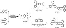
ObjectiveTo obtain novel and efficient thermally activated delayed fluorescence (TADF) materials, BPQPXZ and BPQTPA are synthesized using dibenzopyridoquinoxaline (BPQ) as acceptor (A) and triphenylamine (TPA) and phenoxazine (PXZ) as donors (D). The results show that the two materials have typical delayed fluorescence characteristics, a smaller energy gap (ΔEST) between singlet and triplet states, and a larger oscillator strength ( f ). The device based on BPQPXZ combined with a strong acceptor and a strong donor achieves deep-red emission with λEL at 660 nm. However, due to the influence of the energy-gap law, the external quantum efficiency (EQE) is only 1.0%. BPQTPA combined with a strong acceptor and a weak donor has a larger fluorescence quantum yield (82.7%) because of the weaker rigidity of TPA than that of PXZ. As a result, the donor and acceptor of BPQTPA have less distortion, more orbital overlap, and larger f . At the same time, the intramolecular charge transfer effect of BPQTPA is weakened, and the electron-donating ability of TPA is weaker than that of PXZ. BPQTPA exhibits a blue-shifted emission compared with BPQPXZ. Therefore, the device based on BPQTPA exhibits yellow emission with λEL at 555 nm. Compared with BPQPXZ, the turn-on voltage of BPQTPA is reduced to 2.8 V; the maximum current efficiency and power efficiency are increased by 32-fold and 36-fold, respectively, and the EQE is increased by 6-fold to 7.0%.MethodsIn this study, BPQPXZ and BPQTPA materials are synthesized using the Suzuki reaction and Buchwald-Hartwig reaction. The photophysical properties, electrochemical properties, thermal properties, and device performance of the two materials are investigated. Comparative analysis is conducted on the luminescent properties of two materials.Results and DiscussionsThe structures of two materials, BPQPXZ and BPQTPA, are verified by 1H nuclear magnetic resonance (1H NMR) spectroscopy and high-resolution mass spectrometry (HRMS). BPQPXZ exhibits deep-red emission with λPL at 655 nm, and BPQTPA exhibits yellow emission with λPL at 585 nm (Fig. 3). Compared with BPQPXZ, BPQTPA exhibits blue-shifted emission because of weaker electron-donating ability of TPA than PXZ. Similarly, the rigidity of TPA is weaker than that of PXZ, resulting in a greater degree of overlap between the HOMO and LUMO of BPQTPA, a higher oscillator strength, and a larger fluorescence quantum yield (82.7%) for BPQTPA, which is consistent with the density functional theory simulation results (Fig. 2). As shown in the transient PL decay spectra (Fig. 4), the delay component is observed, and such phenomena are typical behaviors of TADF. As shown in the cyclic voltammogram (Fig. 5), the HOMO levels of BPQTPA and BPQPXZ are -5.38 eV and -5.25 eV, respectively. The calculated LUMO levels are -3.00 eV and -3.27 eV for BPQTPA and BPQPXZ, respectively. BPQTPA shows better thermal stability with a higher decomposition temperature (Td, with 5% weight loss) of 492.6 ℃ than BPQPXZ (Td=439.2 ℃). The higher thermal stability of BPQTPA can be ascribed to its better planarity than that of BPQPXZ. These devices based on BPQTPA and BPQPXZ achieve good performance (Fig. 7). The device based on BPQTPA exhibits much higher EQE (7.0%) than the device based on BPQPXZ (EQE is 1.0%), especially.ConclusionsIn this study, BPQTPA and BPQPXZ materials are designed and synthesized using BPQ with a highly rigid conjugated planar structure as an acceptor and TPA and PXZ as donors. The results show that two materials have typical delayed fluorescence characteristics. BPQTPA and BPQPXZ achieve good orbital separation between HOMO and LUMO, as well as a certain degree of orbital overlap, resulting in a smaller ΔEST and a larger oscillator strength. The device based on BPQPXZ combined with a strong acceptor and a strong donor achieves deep-red emission with λEL at 660 nm. However, due to the influence of energy-gap law, non-radiative decay is serious, with an EQE of only 1.0%, as well as low current and power efficiency. The device based on BPQTPA combined with a strong acceptor and a weak donor is less rigid than that based on BPQPXZ, making the degree of donor and acceptor distortion of BPQTPA less than BPQPXZ, and the degree of overlap between HOMO and LUMO orbitals of BPQTPA increases, so oscillator strength of BPQTPA is 2.2 times that of BPQPXZ. As a result, BPQTPA has a higher PLQY (82.7%). Meanwhile, due to the much weaker electron-donating ability of TPA than PXZ, the intramolecular charge transfer effect of BPQTPA is weakened, resulting in a significant blue-shift in both photoluminescence and electroluminescence peaks. The device based on BPQTPA exhibits yellow emission with λEL at 555 nm. Compared with BPQPXZ, the turn-on voltage of the device based on BPQTPA is reduced to 2.8 V, and the current efficiency and power efficiency are significantly improved by 32-fold and 36-fold, respectively. The EQE is increased by 6-fold to 7.0%. In particular, we investigate the effects of reasonable combinations of donor and acceptor on the photophysical and electroluminescent properties of materials through structure-activity relationships, and the study is of certain reference significance for the research on long-wavelength TADF materials. ObjectiveTo obtain novel and efficient thermally activated delayed fluorescence (TADF) materials, BPQPXZ and BPQTPA are synthesized using dibenzopyridoquinoxaline (BPQ) as acceptor (A) and triphenylamine (TPA) and phenoxazine (PXZ) as donors (D). The results show that the two materials have typical delayed fluorescence characteristics, a smaller energy gap (ΔEST) between singlet and triplet states, and a larger oscillator strength ( f ). The device based on BPQPXZ combined with a strong acceptor and a strong donor achieves deep-red emission with λEL at 660 nm. However, due to the influence of the energy-gap law, the external quantum efficiency (EQE) is only 1.0%. BPQTPA combined with a strong acceptor and a weak donor has a larger fluorescence quantum yield (82.7%) because of the weaker rigidity of TPA than that of PXZ. As a result, the donor and acceptor of BPQTPA have less distortion, more orbital overlap, and larger f . At the same time, the intramolecular charge transfer effect of BPQTPA is weakened, and the electron-donating ability of TPA is weaker than that of PXZ. BPQTPA exhibits a blue-shifted emission compared with BPQPXZ. Therefore, the device based on BPQTPA exhibits yellow emission with λEL at 555 nm. Compared with BPQPXZ, the turn-on voltage of BPQTPA is reduced to 2.8 V; the maximum current efficiency and power efficiency are increased by 32-fold and 36-fold, respectively, and the EQE is increased by 6-fold to 7.0%.MethodsIn this study, BPQPXZ and BPQTPA materials are synthesized using the Suzuki reaction and Buchwald-Hartwig reaction. The photophysical properties, electrochemical properties, thermal properties, and device performance of the two materials are investigated. Comparative analysis is conducted on the luminescent properties of two materials.Results and DiscussionsThe structures of two materials, BPQPXZ and BPQTPA, are verified by 1H nuclear magnetic resonance (1H NMR) spectroscopy and high-resolution mass spectrometry (HRMS). BPQPXZ exhibits deep-red emission with λPL at 655 nm, and BPQTPA exhibits yellow emission with λPL at 585 nm (Fig. 3). Compared with BPQPXZ, BPQTPA exhibits blue-shifted emission because of weaker electron-donating ability of TPA than PXZ. Similarly, the rigidity of TPA is weaker than that of PXZ, resulting in a greater degree of overlap between the HOMO and LUMO of BPQTPA, a higher oscillator strength, and a larger fluorescence quantum yield (82.7%) for BPQTPA, which is consistent with the density functional theory simulation results (Fig. 2). As shown in the transient PL decay spectra (Fig. 4), the delay component is observed, and such phenomena are typical behaviors of TADF. As shown in the cyclic voltammogram (Fig. 5), the HOMO levels of BPQTPA and BPQPXZ are -5.38 eV and -5.25 eV, respectively. The calculated LUMO levels are -3.00 eV and -3.27 eV for BPQTPA and BPQPXZ, respectively. BPQTPA shows better thermal stability with a higher decomposition temperature (Td, with 5% weight loss) of 492.6 ℃ than BPQPXZ (Td=439.2 ℃). The higher thermal stability of BPQTPA can be ascribed to its better planarity than that of BPQPXZ. These devices based on BPQTPA and BPQPXZ achieve good performance (Fig. 7). The device based on BPQTPA exhibits much higher EQE (7.0%) than the device based on BPQPXZ (EQE is 1.0%), especially.ConclusionsIn this study, BPQTPA and BPQPXZ materials are designed and synthesized using BPQ with a highly rigid conjugated planar structure as an acceptor and TPA and PXZ as donors. The results show that two materials have typical delayed fluorescence characteristics. BPQTPA and BPQPXZ achieve good orbital separation between HOMO and LUMO, as well as a certain degree of orbital overlap, resulting in a smaller ΔEST and a larger oscillator strength. The device based on BPQPXZ combined with a strong acceptor and a strong donor achieves deep-red emission with λEL at 660 nm. However, due to the influence of energy-gap law, non-radiative decay is serious, with an EQE of only 1.0%, as well as low current and power efficiency. The device based on BPQTPA combined with a strong acceptor and a weak donor is less rigid than that based on BPQPXZ, making the degree of donor and acceptor distortion of BPQTPA less than BPQPXZ, and the degree of overlap between HOMO and LUMO orbitals of BPQTPA increases, so oscillator strength of BPQTPA is 2.2 times that of BPQPXZ. As a result, BPQTPA has a higher PLQY (82.7%). Meanwhile, due to the much weaker electron-donating ability of TPA than PXZ, the intramolecular charge transfer effect of BPQTPA is weakened, resulting in a significant blue-shift in both photoluminescence and electroluminescence peaks. The device based on BPQTPA exhibits yellow emission with λEL at 555 nm. Compared with BPQPXZ, the turn-on voltage of the device based on BPQTPA is reduced to 2.8 V, and the current efficiency and power efficiency are significantly improved by 32-fold and 36-fold, respectively. The EQE is increased by 6-fold to 7.0%. In particular, we investigate the effects of reasonable combinations of donor and acceptor on the photophysical and electroluminescent properties of materials through structure-activity relationships, and the study is of certain reference significance for the research on long-wavelength TADF materials.
Acta Optica Sinica
- Publication Date: Apr. 25, 2024
- Vol. 44, Issue 8, 0816001 (2024)


Numerical Simulation of Temperature Distribution in End-Pumped Nd∶YAG with Uniform and Gradient Dopants of Nd3+
Fangfang Ruan, Fangying Tang, Jinhong Wang, Lü Yanfei, Jiawei Li, Xinxin Wang, Yuhui Yan, Liangbi Su, and Lihe Zheng
The temperature decrease rate in bulk Nd∶YAG is 34 ℃/mm along the radial direction from the central axis of Nd∶YAG to the thermal sink copper. In the case of gradient Nd∶YAG, the temperature decreasing rate is around 14 ℃/mm.ObjectiveNd∶YAG with a uniform dopant of Nd3+ can generate gradient temperature distribution along laser propagation under high-power semiconductor diode lasers (LDs), which may cause a thermal lens effect, and thus reduce laser output power and beam quality. Regulating the gradient dopant of Nd3+ in Nd∶YAG is paid great attention to for improving the efficiency and beam quality. The traditional regulation method is to fabricate Nd∶YAG with gradient dopant by a unique dual-crucible technology from the Czochralski method. With the development of room temperature bonding technology, it is flexible to obtain designed gradient dopants of Nd3+ with specific sample thicknesses in a monolithic structure. We propose a numerical simulation method by establishing heat source equations. The temperature distribution in Nd∶YAG with uniform and gradient dopants of Nd3+ under kilowatt pump power is reported accordingly. We hope that the basic strategy can help design a new gradient doped Nd∶YAG monolithic gain media and understand the relationship between temperature distribution and Nd∶YAG with specific dopants along laser propagation.MethodsNd∶YAG is employed for numerical simulation of temperature distribution along laser propagation under high pump power. The aperture of Nd∶YAG is 10 mm×10 mm cut along the crystallographic axis [100]. In the case of bulk Nd∶YAG with a uniform dopant of Nd3+, the absorption coefficient is set as 5.78 cm-1 with a bulk length of 8 mm to ensure over 99% absorption of the pump light after single path propagation. In the case of gradient Nd∶YAG, each segment has 1 mm thickness and various absorption coefficients. Meanwhile, a quarter geometric model is built to compare the temperature distribution in the central axis of bulk Nd∶YAG and gradient Nd∶YAG along laser propagation. The initial pump power is 1000 W and the pump pulse width time is 46 μs, with the repetition frequency of 1 kHz. The flat-top pump light is employed for temperature distribution calculation and heat source expression.Results and DiscussionsFollowing the pump energy of 46 mJ at 1 kHz, the temperature distribution along laser propagation in the central axis of bulk Nd∶YAG decreases from 185 to 26 ℃. The temperature is reduced to 106, 51, and 29 ℃ at the positions of 2, 4, and 6 mm in bulk Nd∶YAG, respectively. This indicates that the temperature close to the pump light is the highest in a bulk Nd∶YAG. By adjusting the absorption coefficient to 1.5, 2.1, 3.3, and 9.7 cm-1 for each segment with 1 mm thickness in gradient Nd∶YAG, the constant distribution of temperature around 86.5 ℃ is obtained. The maximum temperature is 88.5 ℃ when the temperature difference between maximum and minimum value is 7.5 ℃. Additionally, by properly designing the sample thickness and absorption coefficient of the gradient Nd∶YAG, the total thickness can be shortened to 4 mm, which is beneficial for ultrashort pulse generation in microcavity.ConclusionsA numerical simulation method by establishing heat source equations is proposed for temperature distribution evaluation in bulk Nd∶YAG and gradient Nd∶YAG. The temperature distribution in gradient Nd∶YAG shows a constant distribution of temperature around 86.5 ℃ under pump energy of 46 mJ at a repetition rate of 1 kHz. This confirms that the design of monolithic gain media such as gradient Nd∶YAG can help understand the temperature distribution along the central axis of Nd∶YAG along laser propagation. The temperature decrease rate in bulk Nd∶YAG is 34 ℃/mm along the radial direction from the central axis of Nd∶YAG to the thermal sink copper. In the case of gradient Nd∶YAG, the temperature decreasing rate is around 14 ℃/mm.ObjectiveNd∶YAG with a uniform dopant of Nd3+ can generate gradient temperature distribution along laser propagation under high-power semiconductor diode lasers (LDs), which may cause a thermal lens effect, and thus reduce laser output power and beam quality. Regulating the gradient dopant of Nd3+ in Nd∶YAG is paid great attention to for improving the efficiency and beam quality. The traditional regulation method is to fabricate Nd∶YAG with gradient dopant by a unique dual-crucible technology from the Czochralski method. With the development of room temperature bonding technology, it is flexible to obtain designed gradient dopants of Nd3+ with specific sample thicknesses in a monolithic structure. We propose a numerical simulation method by establishing heat source equations. The temperature distribution in Nd∶YAG with uniform and gradient dopants of Nd3+ under kilowatt pump power is reported accordingly. We hope that the basic strategy can help design a new gradient doped Nd∶YAG monolithic gain media and understand the relationship between temperature distribution and Nd∶YAG with specific dopants along laser propagation.MethodsNd∶YAG is employed for numerical simulation of temperature distribution along laser propagation under high pump power. The aperture of Nd∶YAG is 10 mm×10 mm cut along the crystallographic axis [100]. In the case of bulk Nd∶YAG with a uniform dopant of Nd3+, the absorption coefficient is set as 5.78 cm-1 with a bulk length of 8 mm to ensure over 99% absorption of the pump light after single path propagation. In the case of gradient Nd∶YAG, each segment has 1 mm thickness and various absorption coefficients. Meanwhile, a quarter geometric model is built to compare the temperature distribution in the central axis of bulk Nd∶YAG and gradient Nd∶YAG along laser propagation. The initial pump power is 1000 W and the pump pulse width time is 46 μs, with the repetition frequency of 1 kHz. The flat-top pump light is employed for temperature distribution calculation and heat source expression.Results and DiscussionsFollowing the pump energy of 46 mJ at 1 kHz, the temperature distribution along laser propagation in the central axis of bulk Nd∶YAG decreases from 185 to 26 ℃. The temperature is reduced to 106, 51, and 29 ℃ at the positions of 2, 4, and 6 mm in bulk Nd∶YAG, respectively. This indicates that the temperature close to the pump light is the highest in a bulk Nd∶YAG. By adjusting the absorption coefficient to 1.5, 2.1, 3.3, and 9.7 cm-1 for each segment with 1 mm thickness in gradient Nd∶YAG, the constant distribution of temperature around 86.5 ℃ is obtained. The maximum temperature is 88.5 ℃ when the temperature difference between maximum and minimum value is 7.5 ℃. Additionally, by properly designing the sample thickness and absorption coefficient of the gradient Nd∶YAG, the total thickness can be shortened to 4 mm, which is beneficial for ultrashort pulse generation in microcavity.ConclusionsA numerical simulation method by establishing heat source equations is proposed for temperature distribution evaluation in bulk Nd∶YAG and gradient Nd∶YAG. The temperature distribution in gradient Nd∶YAG shows a constant distribution of temperature around 86.5 ℃ under pump energy of 46 mJ at a repetition rate of 1 kHz. This confirms that the design of monolithic gain media such as gradient Nd∶YAG can help understand the temperature distribution along the central axis of Nd∶YAG along laser propagation.
Acta Optica Sinica
- Publication Date: Apr. 10, 2024
- Vol. 44, Issue 7, 0716002 (2024)
Fabrication and Mid-Infrared Laser Transmission Performance of Ultra-Low Loss Chalcogenide Glass Fibers
Yantao Xu, Haitao Guo, Xusheng Xiao, Man Li, and Mengmeng Yan
ObjectiveWith the continuous development of infrared optics, the demand for infrared laser transmission in such fields as national defense and security, biomedicine, and advanced manufacturing is becoming increasingly urgent, and therefore infrared energy transmission fibers are receiving increasing attention. The chalcogenide glass, as an excellent infrared material, features a wide transmission range, stable physic-chemical properties, and easy fiber formation, which makes it an ideal material for infrared energy transmission fibers. The high optical loss of domestically produced chalcogenide glass fibers currently limits their widespread applications. The origin of the optical loss for chalcogenide glass fibers mainly includes the absorption loss of C, H, O, and other impurities; scattering loss caused by heterogeneous particle impurities and striae; scattering loss caused by the interface defects between the core and cladding. For suppressing the absorption loss and scattering loss in chalcogenide glasses and obtaining ultra-low loss fibers, gas (chlorine gas)-gas (glass vapor) and solid (aluminum)-liquid (glass melt) chemical reactions are employed to reduce the absorption loss of fibers. A three-dimensional laser microscopic imaging system is established and adopted to detect micron- and submicron-sized defects inside the glass and fiber, and the preparation process is correspondingly optimized to reduce the scattering loss of fibers. The laser energy transmission experiments of fiber laser (wavelength is 2.0 μm) and dual wavelength optical parameter oscillator (OPO) laser (wavelength is 3.8 μm and 4.7 μm) are also carried out.MethodsHigh purity S and As elements are utilized to prepare rod (As40S60) and tube (As39S61). S distilled at 200 ℃ and As sublimed at 350 ℃ are encapsulated in the ampoule and then melted at 750 ℃ for 12 h to obtain preform glasses. Further, hydrogen impurities with the high purity Cl2 are eliminated. Cl2 is introduced into the molten glass and the quantity of flow is 5 ml/min for 300-600 s. The glass is melted again to allow a reaction between the Cl2 and hydrogen ions. Then the melted product is distilled under a dynamic vacuum to eliminate any gaseous byproducts from the reaction with Cl2. The third step is to eliminate oxygen impurities with elemental aluminum. Al foils with a mass fraction of 0.3% are introduced into the glass and melted at 600 ℃. Oxygen impurities react with Al foils to form Al2O3 which is left on the surface of Al foils, thus obtaining high-purity glasses. The optical fiber is prepared by the rod-in-tube method. The core and cladding diameters are 200 μm/250 μm for multi-mode fiber and 9 μm/140 μm for single-mode fiber, respectively. The single-mode fiber can maintain single-mode transmission in the 3-5 μm band. The fiber is drawn at about 320 ℃ in a nitrogen-protected environment. The optical fiber loss is measured by the cutback technique and the scattering intensity of the chalcogenide glasses and fibers are examined by a highly sensitive InGaAs detector from the direction perpendicular to the light path (Fig. 4).Results and DiscussionsThe additive amounts of Cl2 are 300, 480, and 600 s, and the samples are recorded as C1, C2, and C3, respectively. The absorption spectra of C1, C2, and C3 samples show that with the increasing Cl2, the absorption intensity at 4.1 μm decreases significantly while the absorption intensity rises gradually at 7.6 μm (Fig. 5). Hydrogen impurities are effectively removed when Cl2 is employed to purify the chalcogenide glasses for reducing the H—S absorption at 4.1 μm. However, more oxygen impurities are also introduced into the glass due to the hydrophility of Cl2, which enhances the absorption intensity of As—O impurities at 7.6 μm. For further elimination of oxygen impurities, aluminum is introduced into the C3 glass, with the sample signed as C3A. The absorption intensity at 7.6 μm decreases significantly and the mass fraction of oxygen impurities reduces from 1.55% to 0.22% (Fig. 6). There is a linear relationship between the mass fraction of oxygen and absorption coefficient at 7.6 μm in chalcogenide glasses (Fig. 7). The striae of the glass is compared for three samples quenched from three different temperatures of 400, 450, and 500 ℃, and the results show that the sample quenched at 450 ℃ has the best uniformity (Fig. 8). The scattering intensity of these three samples also confirms the above conclusions. The gray values of the scattering image for samples quenched at 450 ℃ are more concentrated in the low grade region, which means that the background scattering intensity at 450 ℃ is the lowest (Fig. 9). The fiber attenuation is 0.150 dB/m, 0.087 dB/m at 4.778 μm for C3 and C3A samples respectively (Fig. 11). A laser power output of 6.10 W is obtained in a single-mode fiber when the input power is 12.30 W at 2.0 μm wavelength. The transmission efficiency is about 50%. The output power of 6.12 W is obtained in a multi-mode fiber when the input power is 10.20 W at 3.8 μm and 4.7 μm wavelength. The transmission efficiency is about 59% (Fig. 13).ConclusionsThe purification technique of chalcogenide glasses is studied. Cl2 is introduced in chalcogenide glasses to eliminate the hydrogen impurities, and the absorption caused by hydrogen impurities decreases with the Cl2 input volume. However, the As—O absorption intensity rises gradually at 7.6 μm, and the absorption coefficient is linearly proportional to the mass fraction of oxygen. The mass fraction of oxygen impurity in the glass is reduced from 1.55% to 0.22% by introducing the reducing agent aluminum. A detection system is set up for examining the defects in the glass using the scattering technique. The glass quenched at 450 ℃ has the least defects. The glass fiber with a loss of 0.087 dB/m (@4.778 μm) is prepared. The output power of 6.10 W is obtained when the input power is 12.30 W at 2.0 μm wavelength for single-mode fiber, and the transmission efficiency is about 50%. Meanwhile, the transmission efficiency is about 59% for multi-mode fiber at 3.8 μm and 4.7 μm wavelength. The laser damage of the end face is mainly caused by the position deviation generated by thermal expansion, which restricts the transmission power of optical fibers. The transmission power of optical fibers is expected to be further improved by adding a fiber cooling system and reducing energy penetration. ObjectiveWith the continuous development of infrared optics, the demand for infrared laser transmission in such fields as national defense and security, biomedicine, and advanced manufacturing is becoming increasingly urgent, and therefore infrared energy transmission fibers are receiving increasing attention. The chalcogenide glass, as an excellent infrared material, features a wide transmission range, stable physic-chemical properties, and easy fiber formation, which makes it an ideal material for infrared energy transmission fibers. The high optical loss of domestically produced chalcogenide glass fibers currently limits their widespread applications. The origin of the optical loss for chalcogenide glass fibers mainly includes the absorption loss of C, H, O, and other impurities; scattering loss caused by heterogeneous particle impurities and striae; scattering loss caused by the interface defects between the core and cladding. For suppressing the absorption loss and scattering loss in chalcogenide glasses and obtaining ultra-low loss fibers, gas (chlorine gas)-gas (glass vapor) and solid (aluminum)-liquid (glass melt) chemical reactions are employed to reduce the absorption loss of fibers. A three-dimensional laser microscopic imaging system is established and adopted to detect micron- and submicron-sized defects inside the glass and fiber, and the preparation process is correspondingly optimized to reduce the scattering loss of fibers. The laser energy transmission experiments of fiber laser (wavelength is 2.0 μm) and dual wavelength optical parameter oscillator (OPO) laser (wavelength is 3.8 μm and 4.7 μm) are also carried out.MethodsHigh purity S and As elements are utilized to prepare rod (As40S60) and tube (As39S61). S distilled at 200 ℃ and As sublimed at 350 ℃ are encapsulated in the ampoule and then melted at 750 ℃ for 12 h to obtain preform glasses. Further, hydrogen impurities with the high purity Cl2 are eliminated. Cl2 is introduced into the molten glass and the quantity of flow is 5 ml/min for 300-600 s. The glass is melted again to allow a reaction between the Cl2 and hydrogen ions. Then the melted product is distilled under a dynamic vacuum to eliminate any gaseous byproducts from the reaction with Cl2. The third step is to eliminate oxygen impurities with elemental aluminum. Al foils with a mass fraction of 0.3% are introduced into the glass and melted at 600 ℃. Oxygen impurities react with Al foils to form Al2O3 which is left on the surface of Al foils, thus obtaining high-purity glasses. The optical fiber is prepared by the rod-in-tube method. The core and cladding diameters are 200 μm/250 μm for multi-mode fiber and 9 μm/140 μm for single-mode fiber, respectively. The single-mode fiber can maintain single-mode transmission in the 3-5 μm band. The fiber is drawn at about 320 ℃ in a nitrogen-protected environment. The optical fiber loss is measured by the cutback technique and the scattering intensity of the chalcogenide glasses and fibers are examined by a highly sensitive InGaAs detector from the direction perpendicular to the light path (Fig. 4).Results and DiscussionsThe additive amounts of Cl2 are 300, 480, and 600 s, and the samples are recorded as C1, C2, and C3, respectively. The absorption spectra of C1, C2, and C3 samples show that with the increasing Cl2, the absorption intensity at 4.1 μm decreases significantly while the absorption intensity rises gradually at 7.6 μm (Fig. 5). Hydrogen impurities are effectively removed when Cl2 is employed to purify the chalcogenide glasses for reducing the H—S absorption at 4.1 μm. However, more oxygen impurities are also introduced into the glass due to the hydrophility of Cl2, which enhances the absorption intensity of As—O impurities at 7.6 μm. For further elimination of oxygen impurities, aluminum is introduced into the C3 glass, with the sample signed as C3A. The absorption intensity at 7.6 μm decreases significantly and the mass fraction of oxygen impurities reduces from 1.55% to 0.22% (Fig. 6). There is a linear relationship between the mass fraction of oxygen and absorption coefficient at 7.6 μm in chalcogenide glasses (Fig. 7). The striae of the glass is compared for three samples quenched from three different temperatures of 400, 450, and 500 ℃, and the results show that the sample quenched at 450 ℃ has the best uniformity (Fig. 8). The scattering intensity of these three samples also confirms the above conclusions. The gray values of the scattering image for samples quenched at 450 ℃ are more concentrated in the low grade region, which means that the background scattering intensity at 450 ℃ is the lowest (Fig. 9). The fiber attenuation is 0.150 dB/m, 0.087 dB/m at 4.778 μm for C3 and C3A samples respectively (Fig. 11). A laser power output of 6.10 W is obtained in a single-mode fiber when the input power is 12.30 W at 2.0 μm wavelength. The transmission efficiency is about 50%. The output power of 6.12 W is obtained in a multi-mode fiber when the input power is 10.20 W at 3.8 μm and 4.7 μm wavelength. The transmission efficiency is about 59% (Fig. 13).ConclusionsThe purification technique of chalcogenide glasses is studied. Cl2 is introduced in chalcogenide glasses to eliminate the hydrogen impurities, and the absorption caused by hydrogen impurities decreases with the Cl2 input volume. However, the As—O absorption intensity rises gradually at 7.6 μm, and the absorption coefficient is linearly proportional to the mass fraction of oxygen. The mass fraction of oxygen impurity in the glass is reduced from 1.55% to 0.22% by introducing the reducing agent aluminum. A detection system is set up for examining the defects in the glass using the scattering technique. The glass quenched at 450 ℃ has the least defects. The glass fiber with a loss of 0.087 dB/m (@4.778 μm) is prepared. The output power of 6.10 W is obtained when the input power is 12.30 W at 2.0 μm wavelength for single-mode fiber, and the transmission efficiency is about 50%. Meanwhile, the transmission efficiency is about 59% for multi-mode fiber at 3.8 μm and 4.7 μm wavelength. The laser damage of the end face is mainly caused by the position deviation generated by thermal expansion, which restricts the transmission power of optical fibers. The transmission power of optical fibers is expected to be further improved by adding a fiber cooling system and reducing energy penetration.
Acta Optica Sinica
- Publication Date: Apr. 10, 2024
- Vol. 44, Issue 7, 0716001 (2024)
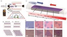
Multiphase Controllable Growth and Second Harmonic Enhancement of Two-Dimensional Semiconductor WSe2
Guang Wang, Bowen Yao, and Lü Zhiquan
ObjectiveIn recent years, there have been many studies on the preparation of high-quality transition-metal dichalcogenides (TMDCs), which have a variety of applications including optoelectronics, spin-tronics, and valleytronics. The most attractive properties of TMDCs as candidates for such diverse applications are layer and phase dependence. Therefore, the controlled growth of various phases of TMDCs and the stacking of distinct layers have emerged as popular research realms. In previous research, people have summarized the theory of supersaturation-dependent crystal growth by continuously refining the classical BCF (Burton-Cabrera-Frank) theory. However, on the one hand, supersaturation-dependent growth theory is often employed to provide a theoretical interpretation for preparing a certain phase that lacks systematicity, and on the other hand, the parameter control involved in such theories is difficult to measure and regulate experimentally. Our study focuses on controlling the temperature distribution to affect the supersaturation degree and achieve the one-step controllable growth of three phases of WSe2 (single layer, 3R, and 2H) directly on the different regions at the substrate under a temperature gradient. By regulating the temperature distribution, we can change the supersaturation distribution and successfully prepare spiral plates of WSe2 by screw-dislocation-driven (SDD) growth mode, transitioning from layer-by-layer (LBL) growth mode, where we observe two orders of magnitude of second harmonic generation (SHG) signal enhancement in the spiral-stacked region. These different vertically stacked TMDCs materials will offer diverse candidates for probing the physical properties of layered materials and exploring new applications in functional electronic and optoelectronic devices.MethodsOur experiments adopt the reverse flow method to control the growth time and growth temperature in the growth process and shorten the cooling time by a rapid cooling method. With the help of the supersaturation-dependent crystal growth theory and our experimental methods, we establish a connection between the temperature distribution, supersaturation distribution, and growth result distribution (Figs. 1 and 3). By the morphological characterization (Figs. 1 and 3) such as optic microscope (OM), atomic force microscopy (AFM), and scanning electron micrographs (SEM), we analyze the stacking mode of samples. Meanwhile, we further analyze the optical properties of the samples and demonstrate the growth of spiral structures by the spectroscopic (Figs. 2 and 4) characterization such as the Raman spectrum, photo luminescence (PL) spectrum, SHG spectrum, and spectrum mapping.Results and DiscussionsWe successfully prepare monolayer, 2H-phase , and 3R-phase of WSe2 in our supersaturation-controlled growth experiments and demonstrate their distributions [Fig. 1 (c)]. Due to the different atomic structures of the two stacking phases [Figs. 1 (d) and (e)], they exhibit different morphologies under OM, and AFM [Figs. 1 (f)-(m), Figs. 2 (a)-(c)]. Different atomic structures in different stacks will produce different electronic structures to affect the optical properties of the material. To reveal different-induced interlayer coupling in the 3R-phase and 2H-phase WSe2, we perform PL and Raman spectroscopy on both stacking and single layer regions. The Raman spectrum of the two phases reveals different trends with increasing stacking layers, generated by different interlayer coupling [Figs. 2 (d) and (e)]. The indirect bandgap transition can be observed in the stacking area [Fig. 2 (f)], which originates from the interlayer electronic coupling. The indirect transition energy reflects the stability of the electronic structure and the strength of interlayer coupling: the lower transition energy means more stable electronic structure and stronger interlayer coupling, which is also reflected in our growth results. We show the above conclusions more vividly by spectrum mapping [Figs. 2 (g)-(i) and Figs. 2 (k)-(m)]. Symmetry also affects interlayer coupling, which will be displayed by SHG mapping. According to the supersaturation-dependent crystal growth theory, the growth mode transition from LBL to SDD is attributed to the changing supersaturation distribution. The different saturation distributions will also affect the complexity in SDD mode, which is demonstrated by OM and AFM (Fig. 3). After observing the emergence of the spiral structure, we investigate it by spectroscopy method. Similar to the Raman spectrum of 3R-phase WSe2 under the interlayer coupling, the Raman signal of the spiral WSe2 is also manifested as the weakened trends with the increasing number of stacking layers [Fig. 4 (a)]. In addition to interlayer coupling, the strain also has a significant influence on the optical properties of the spiral WSe2, which is evidenced by the continuum changes of the PL spectral and aberrations in the polarization SHG [Figs. 4 (b), (i), and (l)]. According to the spectroscopic law of stacked WSe2 discussed previously, we demonstrate the growth kinetics of the two-armd spiral structure by PL and SHG mapping [Figs. 4 (c)-(h) and Fig. 4 (k)]. Towards the armchair direction, we find two orders of magnitude SHG enhancement in the center position [Fig. 4 (j)].ConclusionsBy adopting the reverse flow chemical vapor deposition strategy, we accurately control the gradient distribution of the growth temperature, which determines the supersaturation distribution. The controllable growth of single layer, 2H-phase, 3R-phase, and spiral structure WSe2 is realized. Additionally, we demonstrate the growth process of the spiral structure and elucidate the effect of interlayer coupling and strain on the optical properties of stacking WSe2 via morphological and spectroscopic characterization. Thesupersaturation-dependent crystal growth theory is utilized to analyze the relationship between the number of screw-dislocation arms of spiral WSe2 and different supersaturation distributions. Meanwhile, we find two orders of magnitude in the center of spiral WSe2, and our study paves the way for two-dimensional semiconductor multi-phase controlling growth, structural design, stacking optical properties regulation, and optoelectronic devices. ObjectiveIn recent years, there have been many studies on the preparation of high-quality transition-metal dichalcogenides (TMDCs), which have a variety of applications including optoelectronics, spin-tronics, and valleytronics. The most attractive properties of TMDCs as candidates for such diverse applications are layer and phase dependence. Therefore, the controlled growth of various phases of TMDCs and the stacking of distinct layers have emerged as popular research realms. In previous research, people have summarized the theory of supersaturation-dependent crystal growth by continuously refining the classical BCF (Burton-Cabrera-Frank) theory. However, on the one hand, supersaturation-dependent growth theory is often employed to provide a theoretical interpretation for preparing a certain phase that lacks systematicity, and on the other hand, the parameter control involved in such theories is difficult to measure and regulate experimentally. Our study focuses on controlling the temperature distribution to affect the supersaturation degree and achieve the one-step controllable growth of three phases of WSe2 (single layer, 3R, and 2H) directly on the different regions at the substrate under a temperature gradient. By regulating the temperature distribution, we can change the supersaturation distribution and successfully prepare spiral plates of WSe2 by screw-dislocation-driven (SDD) growth mode, transitioning from layer-by-layer (LBL) growth mode, where we observe two orders of magnitude of second harmonic generation (SHG) signal enhancement in the spiral-stacked region. These different vertically stacked TMDCs materials will offer diverse candidates for probing the physical properties of layered materials and exploring new applications in functional electronic and optoelectronic devices.MethodsOur experiments adopt the reverse flow method to control the growth time and growth temperature in the growth process and shorten the cooling time by a rapid cooling method. With the help of the supersaturation-dependent crystal growth theory and our experimental methods, we establish a connection between the temperature distribution, supersaturation distribution, and growth result distribution (Figs. 1 and 3). By the morphological characterization (Figs. 1 and 3) such as optic microscope (OM), atomic force microscopy (AFM), and scanning electron micrographs (SEM), we analyze the stacking mode of samples. Meanwhile, we further analyze the optical properties of the samples and demonstrate the growth of spiral structures by the spectroscopic (Figs. 2 and 4) characterization such as the Raman spectrum, photo luminescence (PL) spectrum, SHG spectrum, and spectrum mapping.Results and DiscussionsWe successfully prepare monolayer, 2H-phase , and 3R-phase of WSe2 in our supersaturation-controlled growth experiments and demonstrate their distributions [Fig. 1 (c)]. Due to the different atomic structures of the two stacking phases [Figs. 1 (d) and (e)], they exhibit different morphologies under OM, and AFM [Figs. 1 (f)-(m), Figs. 2 (a)-(c)]. Different atomic structures in different stacks will produce different electronic structures to affect the optical properties of the material. To reveal different-induced interlayer coupling in the 3R-phase and 2H-phase WSe2, we perform PL and Raman spectroscopy on both stacking and single layer regions. The Raman spectrum of the two phases reveals different trends with increasing stacking layers, generated by different interlayer coupling [Figs. 2 (d) and (e)]. The indirect bandgap transition can be observed in the stacking area [Fig. 2 (f)], which originates from the interlayer electronic coupling. The indirect transition energy reflects the stability of the electronic structure and the strength of interlayer coupling: the lower transition energy means more stable electronic structure and stronger interlayer coupling, which is also reflected in our growth results. We show the above conclusions more vividly by spectrum mapping [Figs. 2 (g)-(i) and Figs. 2 (k)-(m)]. Symmetry also affects interlayer coupling, which will be displayed by SHG mapping. According to the supersaturation-dependent crystal growth theory, the growth mode transition from LBL to SDD is attributed to the changing supersaturation distribution. The different saturation distributions will also affect the complexity in SDD mode, which is demonstrated by OM and AFM (Fig. 3). After observing the emergence of the spiral structure, we investigate it by spectroscopy method. Similar to the Raman spectrum of 3R-phase WSe2 under the interlayer coupling, the Raman signal of the spiral WSe2 is also manifested as the weakened trends with the increasing number of stacking layers [Fig. 4 (a)]. In addition to interlayer coupling, the strain also has a significant influence on the optical properties of the spiral WSe2, which is evidenced by the continuum changes of the PL spectral and aberrations in the polarization SHG [Figs. 4 (b), (i), and (l)]. According to the spectroscopic law of stacked WSe2 discussed previously, we demonstrate the growth kinetics of the two-armd spiral structure by PL and SHG mapping [Figs. 4 (c)-(h) and Fig. 4 (k)]. Towards the armchair direction, we find two orders of magnitude SHG enhancement in the center position [Fig. 4 (j)].ConclusionsBy adopting the reverse flow chemical vapor deposition strategy, we accurately control the gradient distribution of the growth temperature, which determines the supersaturation distribution. The controllable growth of single layer, 2H-phase, 3R-phase, and spiral structure WSe2 is realized. Additionally, we demonstrate the growth process of the spiral structure and elucidate the effect of interlayer coupling and strain on the optical properties of stacking WSe2 via morphological and spectroscopic characterization. Thesupersaturation-dependent crystal growth theory is utilized to analyze the relationship between the number of screw-dislocation arms of spiral WSe2 and different supersaturation distributions. Meanwhile, we find two orders of magnitude in the center of spiral WSe2, and our study paves the way for two-dimensional semiconductor multi-phase controlling growth, structural design, stacking optical properties regulation, and optoelectronic devices.
Acta Optica Sinica
- Publication Date: Feb. 25, 2024
- Vol. 44, Issue 4, 0416002 (2024)
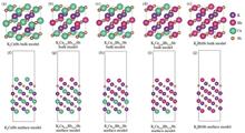
Effect of Rb Doping on Photoelectric Properties of K-Cs-Sb Cathode Material
Yunfeng Han, Muchun Jin, Ling Ren, Xingchao Wang, Kaimin Zhang, Xiaorong Liu, Yunsheng Qian, and Yijun Zhang
ObjectiveAlkali antimonide photocathodes are widely used in many fields such as radiation detection, photon counting, and accelerator electron source due to their advantages of high quantum efficiency, long lifespan, short response time, and low preparation cost. Since K2CsSb bi-alkali photocathode has high photosensitivity ranging from 300 nm to 650 nm, it is often used as the key component of large-area microchannel plate photomultiplier tube and dynode photomultiplier tube. K-Cs-Rb-Sb tri-alkali photocathodes may exhibit more outstanding performance in spectral response enhancement and thermionic emission suppression compared to conventional K2CsSb bi-alkali photocathode. So far, there have been little theoretical researches on K-Cs-Rb-Sb tri-alkali photocathodes. Due to the difficulty in controlling the stoichiometric ratio of alkali metal elements during the actual preparation processes of K-Cs-Rb-Sb photocathodes, and in fact K-Cs-Rb-Sb tri-alkali photocathodes with different stoichiometric ratios have different photoemission properties, it is necessary to analyze the mechanism of Rb doping leading to different photocathode properties from the atomic and electronic perspective, thereby providing theoretical guidance for designing excellent alkali antimonide photocathodes.MethodsThe K2Cs2-xRbxSb bulk models and the (111)-oriented surface models with different Cs/Rb ratios corresponding to K2CsSb,K2Cs0.75Rb0.25Sb,K2Cs0.5Rb0.5Sb,K2Cs0.25Rb0.75Sb,and K2RbSb were established. The K2CsSb unit cell belongs to the DO3 cubic structure with a lattice constant of 0.8615 nm, and the space group is Fm-3m. According to the number of Cs atoms in K2CsSb replaced by Rb atoms, the lattice constants of several K-Cs-Rb-Sb bulk models after atom replacements were obtained by Vegard law. On the basis of the K2CsSb (111) Cs-terminated surface, six, eight, twelve, and sixteen Cs atoms were replaced from top to bottom, to obtain the K-Cs-Rb-Sb(111) surface models with different Cs/Rb ratios. To eliminate inter-layer interactions caused by the periodic mirror interaction between the surface slabs, a vacuum layer of 2 nm was set along the z-axis, including an upper vacuum layer with a thickness of 1.5 nm and a lower vacuum layer with a thickness of 0.5 nm. During the structural optimization process, the upper surface atoms with a thickness of 0.8 nm were allowed to fully relax, while the remaining atoms were constrained. The VASP software package using the first-principles calculation method based on the density functional theory was adopted. The projected augmented wave method was used as the pseudo potential, the generalized gradient approximation function proposed by Perdew-Burke-Ernzerhof was used to express the exchange correlation interaction, the plane wave expansion with a cut-off energy of 500 eV was used, and the conjugate gradient method was used to optimize the lattice constants and atom positions of the diverse models. The K-point grid in the Monkhorst-Pack form was set as 6×6×6 for bulk models and 6×6×1 for surface models, respectively.Results and DiscussionsThe calculation results indicate that when Rb atoms replace Cs atoms in the K-Cs-Rb-Sb bulk models with different Cs/Rb ratios, the optical properties including reflectivity, refractive index, extinction coefficient, and absorption coefficient are hardly affected by Rb doping. This implies that the incorporation of Rb atoms has minimal impact on the optical properties of K2CsSb material. From the perspective of formation energy and formation enthalpy, all the K-Cs-Rb-Sb bulk models where Rb atoms replace K atoms have positive formation energies, and the corresponding formation enthalpies are larger than that of the K2CsSb model. This indicates that it is very difficult for K atoms to be replaced by Rb atoms in the preparation process of K-Cs-Rb-Sb tri-alkali photocathodes. At the same time, all K-Cs-Rb-Sb bulk models where Rb atoms replace Cs atoms have negative formation energies, and the corresponding formation enthalpies are less than that of the K2CsSb model, indicating that all the models where Rb atoms replace Cs atoms are easy to form with better thermodynamic stability. As the number of Rb atoms replacing Cs atoms increases, the formation energies and formation enthalpies gradually decrease. This means that in the presence of both Cs and Rb, the K2Cs0.25Rb0.75Sb model is the easiest to form and the most stable. All K-Cs-Rb-Sb bulk models exhibit the property of p-type semiconductor, and K2Cs0.25Rb0.75Sb has the smallest bandgap. For K-Cs-Rb-Sb surface models with different Cs/Rb ratios, the vacuum levels, surface energies, and electron effective masses gradually decrease. Among them, the K2Cs0.25Rb0.75Sb surface model has the smallest ionization energy, indicating that its electrons generated under external light excitation are more likely to transit from the valence band top to the conduction band bottom and move in the conduction band. This is beneficial for enhancing the spectral response of the photocathode and further improving the photoelectric conversion efficiency. Doping Rb element in K2CsSb can increase the work function of the surface model. On the whole, the K2CsRb0.250.75Sb (111) with a larger work function and surface can prevent the escape of some hot electrons while ensuring that a large number of photoelectrons can escape from the surface, in order to achieve the reduction of cathode dark current without reducing its quantum efficiency. In the surface model containing K, Cs, and Rb alkali metals, K2Cs0.25Rb0.75Sb has the highest conductivity, because the concentration of conduction band electrons gradually increases, and the effective mass of conduction band electrons in the surface model decreases as the number of Cs atoms replaced by Rb atoms increases.ConclusionsWhen Rb atoms replace Cs atoms, Rb doping has little effect on the optical properties of K-Cs-Rb-Sb cathode materials. For K-Cs-Rb-Sb bulk models with different Cs/Rb ratios, K2Cs0.25Rb0.75Sb has the lower formation energy and formation enthalpy, indicating that it is easy to form under natural conditions and it is thermodynamically stable. For the surface models, K2Cs0.25Rb0.75Sb has the smaller surface energy and higher conductivity, as well as the smallest bandgap and ionization energy. Besides, the work function of K2Cs0.25Rb0.75Sb is larger than that of K2CsSb. Therefore, the K-Cs-Rb-Sb cathode with a Cs/Rb ratio (atomic number fraction) of 1∶3 is considered to be a stable photoemission material with high quantum efficiency, low dark current, and good conductivity. The research results can provide guidance for the preparation of high-performance K-Cs-Rb-Sb photocathodes. In the traditional K2CsSb photocathode preparation process, doping Rb elements can reduce the dark noise of the photomultiplier tube while maintaining a high level of quantum efficiency, thereby improving the detection sensitivity and accuracy of the device in practical applications. ObjectiveAlkali antimonide photocathodes are widely used in many fields such as radiation detection, photon counting, and accelerator electron source due to their advantages of high quantum efficiency, long lifespan, short response time, and low preparation cost. Since K2CsSb bi-alkali photocathode has high photosensitivity ranging from 300 nm to 650 nm, it is often used as the key component of large-area microchannel plate photomultiplier tube and dynode photomultiplier tube. K-Cs-Rb-Sb tri-alkali photocathodes may exhibit more outstanding performance in spectral response enhancement and thermionic emission suppression compared to conventional K2CsSb bi-alkali photocathode. So far, there have been little theoretical researches on K-Cs-Rb-Sb tri-alkali photocathodes. Due to the difficulty in controlling the stoichiometric ratio of alkali metal elements during the actual preparation processes of K-Cs-Rb-Sb photocathodes, and in fact K-Cs-Rb-Sb tri-alkali photocathodes with different stoichiometric ratios have different photoemission properties, it is necessary to analyze the mechanism of Rb doping leading to different photocathode properties from the atomic and electronic perspective, thereby providing theoretical guidance for designing excellent alkali antimonide photocathodes.MethodsThe K2Cs2-xRbxSb bulk models and the (111)-oriented surface models with different Cs/Rb ratios corresponding to K2CsSb,K2Cs0.75Rb0.25Sb,K2Cs0.5Rb0.5Sb,K2Cs0.25Rb0.75Sb,and K2RbSb were established. The K2CsSb unit cell belongs to the DO3 cubic structure with a lattice constant of 0.8615 nm, and the space group is Fm-3m. According to the number of Cs atoms in K2CsSb replaced by Rb atoms, the lattice constants of several K-Cs-Rb-Sb bulk models after atom replacements were obtained by Vegard law. On the basis of the K2CsSb (111) Cs-terminated surface, six, eight, twelve, and sixteen Cs atoms were replaced from top to bottom, to obtain the K-Cs-Rb-Sb(111) surface models with different Cs/Rb ratios. To eliminate inter-layer interactions caused by the periodic mirror interaction between the surface slabs, a vacuum layer of 2 nm was set along the z-axis, including an upper vacuum layer with a thickness of 1.5 nm and a lower vacuum layer with a thickness of 0.5 nm. During the structural optimization process, the upper surface atoms with a thickness of 0.8 nm were allowed to fully relax, while the remaining atoms were constrained. The VASP software package using the first-principles calculation method based on the density functional theory was adopted. The projected augmented wave method was used as the pseudo potential, the generalized gradient approximation function proposed by Perdew-Burke-Ernzerhof was used to express the exchange correlation interaction, the plane wave expansion with a cut-off energy of 500 eV was used, and the conjugate gradient method was used to optimize the lattice constants and atom positions of the diverse models. The K-point grid in the Monkhorst-Pack form was set as 6×6×6 for bulk models and 6×6×1 for surface models, respectively.Results and DiscussionsThe calculation results indicate that when Rb atoms replace Cs atoms in the K-Cs-Rb-Sb bulk models with different Cs/Rb ratios, the optical properties including reflectivity, refractive index, extinction coefficient, and absorption coefficient are hardly affected by Rb doping. This implies that the incorporation of Rb atoms has minimal impact on the optical properties of K2CsSb material. From the perspective of formation energy and formation enthalpy, all the K-Cs-Rb-Sb bulk models where Rb atoms replace K atoms have positive formation energies, and the corresponding formation enthalpies are larger than that of the K2CsSb model. This indicates that it is very difficult for K atoms to be replaced by Rb atoms in the preparation process of K-Cs-Rb-Sb tri-alkali photocathodes. At the same time, all K-Cs-Rb-Sb bulk models where Rb atoms replace Cs atoms have negative formation energies, and the corresponding formation enthalpies are less than that of the K2CsSb model, indicating that all the models where Rb atoms replace Cs atoms are easy to form with better thermodynamic stability. As the number of Rb atoms replacing Cs atoms increases, the formation energies and formation enthalpies gradually decrease. This means that in the presence of both Cs and Rb, the K2Cs0.25Rb0.75Sb model is the easiest to form and the most stable. All K-Cs-Rb-Sb bulk models exhibit the property of p-type semiconductor, and K2Cs0.25Rb0.75Sb has the smallest bandgap. For K-Cs-Rb-Sb surface models with different Cs/Rb ratios, the vacuum levels, surface energies, and electron effective masses gradually decrease. Among them, the K2Cs0.25Rb0.75Sb surface model has the smallest ionization energy, indicating that its electrons generated under external light excitation are more likely to transit from the valence band top to the conduction band bottom and move in the conduction band. This is beneficial for enhancing the spectral response of the photocathode and further improving the photoelectric conversion efficiency. Doping Rb element in K2CsSb can increase the work function of the surface model. On the whole, the K2CsRb0.250.75Sb (111) with a larger work function and surface can prevent the escape of some hot electrons while ensuring that a large number of photoelectrons can escape from the surface, in order to achieve the reduction of cathode dark current without reducing its quantum efficiency. In the surface model containing K, Cs, and Rb alkali metals, K2Cs0.25Rb0.75Sb has the highest conductivity, because the concentration of conduction band electrons gradually increases, and the effective mass of conduction band electrons in the surface model decreases as the number of Cs atoms replaced by Rb atoms increases.ConclusionsWhen Rb atoms replace Cs atoms, Rb doping has little effect on the optical properties of K-Cs-Rb-Sb cathode materials. For K-Cs-Rb-Sb bulk models with different Cs/Rb ratios, K2Cs0.25Rb0.75Sb has the lower formation energy and formation enthalpy, indicating that it is easy to form under natural conditions and it is thermodynamically stable. For the surface models, K2Cs0.25Rb0.75Sb has the smaller surface energy and higher conductivity, as well as the smallest bandgap and ionization energy. Besides, the work function of K2Cs0.25Rb0.75Sb is larger than that of K2CsSb. Therefore, the K-Cs-Rb-Sb cathode with a Cs/Rb ratio (atomic number fraction) of 1∶3 is considered to be a stable photoemission material with high quantum efficiency, low dark current, and good conductivity. The research results can provide guidance for the preparation of high-performance K-Cs-Rb-Sb photocathodes. In the traditional K2CsSb photocathode preparation process, doping Rb elements can reduce the dark noise of the photomultiplier tube while maintaining a high level of quantum efficiency, thereby improving the detection sensitivity and accuracy of the device in practical applications.
Acta Optica Sinica
- Publication Date: Feb. 25, 2024
- Vol. 44, Issue 4, 0416001 (2024)

Difference in Extinction Characteristics of Bioparticle Aggregates with Different Monomer Shapes
Guolong Chen, Youlin Gu, Yihua Hu, Fanhao Meng, and Xi Zhang
ObjectiveBiological particle materials have significant wide-band extinction performance, and the monomer shapes of bioparticles are complex with some irregular non-spherical shapes. However, the differences in extinction characteristics of bioparticle aggregates with different monomer shapes are still uncertain and have been ignored in previous research. Thus, we build bioparticle aggregation models with different monomer shapes to calculate the extinction coefficients in the 3-5 μm and 8-14 μm wavebands and analyze the differences in extinction characteristics caused by monomer shapes.MethodsFive typical monomer shapes are constructed by employing multi-sphere models in terms of the scanning electron microscopy (SEM) images, and the complex refractive indices (CRIs) of three biomaterials are calculated according to Kramers-Kronig relations based on specular reflectance in the 2.5-25.0 μm waveband. A novel simulation code or non-spherical particle aggregation (NSPA) model is applied to build realistic spatial structure models of bioparticle aggregates with different monomer shapes. To eliminate the influence of spatial structure density, we select the bioparticle aggregates with the same porosity of 0.840 to obtain the extinction characteristics. The discrete dipole approximation (DDA) method is adopted to calculate average mass extinction coefficient αext, average mass absorption coefficient αabs, and average mass scattering coefficient αsca in the 3-5 μm and 8-14 μm wavebands respectively. Then the differences in extinction characteristics of the bioparticle aggregates with different monomer shapes can be analyzed.Results and DiscussionsAccording to the calculation results, the influence of the monomer size, monomer number, CRI, and aspect ratio (AR) on the absorption and scattering effects of bioparticle aggregates with different monomer shapes is investigated. The results show that the closer size of bioparticle aggregates to the wavelength of incident light leads to stronger scattering of incident light by bioparticle aggregates. For bioparticle materials with monomer particle sizes ranging from 0.5 to 3.0 μm, the extinction ability in the 3-5 μm waveband is significantly stronger than that in the 8-14 μm waveband (Figs. 6 and 7). When the monomer diameter is 2.0 μm, the αext of bioparticle aggregates with different monomer shapes are about 0.820-0.850 m2/g in the 3-5 μm waveband (Fig. 8) and about 0.430-0.470 m2/g in the 8-14 μm waveband (Fig. 9). Within a certain range, an increase in monomer size enhances scattering effects (Fig. 6), but the trend of absorption and scattering effects is usually opposite. In the 3-5 μm waveband, the relative deviation of αext, αabs and αsca can reach about -6%, -1.3%, and -14% respectively (Figs. 6 and 8). In the 8-14 μm waveband, the relative deviation of αext, αabs and αsca can reach about -3.3%, -1.2%, and -14% respectively (Figs. 7 and 9). There are indeed differences in the optical properties of bioparticle aggregates with different monomer shapes. For the bioparticle aggregates with the monomer shape of pancake, when the monomer number is 15, the relative deviation of αext and αsca can reach -2.8% and -6.1%, but under the monomer number of 60, the relative deviation has reduced by more than 50% (Fig. 8). As the monomer number increases, the specific surface area differences of the overall spatial structure among bioparticle aggregates with different monomer shapes become smaller, and the scattering differences of bioparticle aggregates with different monomer shapes are relatively weakened. The extinction abilities of biological particle aggregates are more sensitive to CRI (Figs. 10 and 11). Therefore, the actual relative deviation in the extinction characteristics of bioparticle aggregates is not directly determined by the degree to which the monomer shape deviates from the spherical shape, but by the specific result of the combined effect of absorption and scattering. As the AR of ellipsoid rises, the absorption changes slightly while the scattering ability declines significantly (Figs. 12 and 13). Additionally, the results in the case of similar monomer shapes also demonstrate that the scattering differences caused by monomer shapes are indeed related to the degree to which the monomer shape deviates from the spherical shape.ConclusionsWe construct bioparticle aggregates with five typical monomer shapes and calculate and compare the extinction characteristic parameters of them under the influence of multiple factors. The results indicate that there are great differences in the extinction characteristics of bioparticle aggregates with different monomer shapes, which is mainly caused by the differences in light scattering. Meanwhile, generally the more deviation of the monomer shape from the sphere causes greater differences in extinction characteristic of bioparticle aggregates, but the specific magnitude of the relative deviation of the extinction characteristic parameters is the coupling result of various factors such as monomer size, monomer number, and CRI. Our study is of significance for accurately evaluating and optimizing the extinction performance of biological particle materials. ObjectiveBiological particle materials have significant wide-band extinction performance, and the monomer shapes of bioparticles are complex with some irregular non-spherical shapes. However, the differences in extinction characteristics of bioparticle aggregates with different monomer shapes are still uncertain and have been ignored in previous research. Thus, we build bioparticle aggregation models with different monomer shapes to calculate the extinction coefficients in the 3-5 μm and 8-14 μm wavebands and analyze the differences in extinction characteristics caused by monomer shapes.MethodsFive typical monomer shapes are constructed by employing multi-sphere models in terms of the scanning electron microscopy (SEM) images, and the complex refractive indices (CRIs) of three biomaterials are calculated according to Kramers-Kronig relations based on specular reflectance in the 2.5-25.0 μm waveband. A novel simulation code or non-spherical particle aggregation (NSPA) model is applied to build realistic spatial structure models of bioparticle aggregates with different monomer shapes. To eliminate the influence of spatial structure density, we select the bioparticle aggregates with the same porosity of 0.840 to obtain the extinction characteristics. The discrete dipole approximation (DDA) method is adopted to calculate average mass extinction coefficient αext, average mass absorption coefficient αabs, and average mass scattering coefficient αsca in the 3-5 μm and 8-14 μm wavebands respectively. Then the differences in extinction characteristics of the bioparticle aggregates with different monomer shapes can be analyzed.Results and DiscussionsAccording to the calculation results, the influence of the monomer size, monomer number, CRI, and aspect ratio (AR) on the absorption and scattering effects of bioparticle aggregates with different monomer shapes is investigated. The results show that the closer size of bioparticle aggregates to the wavelength of incident light leads to stronger scattering of incident light by bioparticle aggregates. For bioparticle materials with monomer particle sizes ranging from 0.5 to 3.0 μm, the extinction ability in the 3-5 μm waveband is significantly stronger than that in the 8-14 μm waveband (Figs. 6 and 7). When the monomer diameter is 2.0 μm, the αext of bioparticle aggregates with different monomer shapes are about 0.820-0.850 m2/g in the 3-5 μm waveband (Fig. 8) and about 0.430-0.470 m2/g in the 8-14 μm waveband (Fig. 9). Within a certain range, an increase in monomer size enhances scattering effects (Fig. 6), but the trend of absorption and scattering effects is usually opposite. In the 3-5 μm waveband, the relative deviation of αext, αabs and αsca can reach about -6%, -1.3%, and -14% respectively (Figs. 6 and 8). In the 8-14 μm waveband, the relative deviation of αext, αabs and αsca can reach about -3.3%, -1.2%, and -14% respectively (Figs. 7 and 9). There are indeed differences in the optical properties of bioparticle aggregates with different monomer shapes. For the bioparticle aggregates with the monomer shape of pancake, when the monomer number is 15, the relative deviation of αext and αsca can reach -2.8% and -6.1%, but under the monomer number of 60, the relative deviation has reduced by more than 50% (Fig. 8). As the monomer number increases, the specific surface area differences of the overall spatial structure among bioparticle aggregates with different monomer shapes become smaller, and the scattering differences of bioparticle aggregates with different monomer shapes are relatively weakened. The extinction abilities of biological particle aggregates are more sensitive to CRI (Figs. 10 and 11). Therefore, the actual relative deviation in the extinction characteristics of bioparticle aggregates is not directly determined by the degree to which the monomer shape deviates from the spherical shape, but by the specific result of the combined effect of absorption and scattering. As the AR of ellipsoid rises, the absorption changes slightly while the scattering ability declines significantly (Figs. 12 and 13). Additionally, the results in the case of similar monomer shapes also demonstrate that the scattering differences caused by monomer shapes are indeed related to the degree to which the monomer shape deviates from the spherical shape.ConclusionsWe construct bioparticle aggregates with five typical monomer shapes and calculate and compare the extinction characteristic parameters of them under the influence of multiple factors. The results indicate that there are great differences in the extinction characteristics of bioparticle aggregates with different monomer shapes, which is mainly caused by the differences in light scattering. Meanwhile, generally the more deviation of the monomer shape from the sphere causes greater differences in extinction characteristic of bioparticle aggregates, but the specific magnitude of the relative deviation of the extinction characteristic parameters is the coupling result of various factors such as monomer size, monomer number, and CRI. Our study is of significance for accurately evaluating and optimizing the extinction performance of biological particle materials.
Acta Optica Sinica
- Publication Date: Feb. 10, 2024
- Vol. 44, Issue 3, 0316001 (2024)
Preparation and Optical Properties of Bi2Ga3.985O9∶1.5%Fe3+,Eu3+ Persistent Luminescent Nanoparticles
Aiwaili Ruxiangul, Yanmei Sun, Nuermaiti Kuerbanjiang, Tianqi Zhao, Abdurahman Renagul, and Xuebo Yin
ObjectiveNear-infrared (NIR) persistent luminescence nanoparticles (PLNPs) with strong tissue penetration can avoid light scattering and fluoresce interference of tissues caused by in situ excitation, and they can be employed in the research on biological imaging and tumor diagnosis and treatment. Currently, the majority of reported PLNPs are based on Cr3+ as luminescent centers. The toxicity of heavy metal Cr3+-doped materials poses a potential safety hazard to long-term in vivo imaging tracking and therapy. However, Fe3+ as a basic element of the human body is a good candidate for NIR luminescence center with broadband emission. The longer and stronger emission wavelength of NIR, coupled with its superior penetration ability, further enhances the tissue penetration depth for biological applications. Thus, it is imperative to develop a friendly NIR-PLNP with enhanced luminescence performance for Fe3+-doped materials. We aim to develop Bi2Ga3.985O9∶1.5%Fe3+, 1%Eu3+ (BGO∶1.5%Fe3+, 1%Eu3+) NIR-emission PLNP materials with stronger luminescence intensity and longer emission wavelength by co-doping Eu3+ ions based on BGO∶1.5%Fe3+ PLNP material. The prepared PLNP has excellent NIR luminescence and plays an important role in the in-vivo imaging without background noise and deep tissues.MethodsBGO∶1.5%Fe3+,xEu3+ (x=0-2%) PLNP materials are prepared by the co-precipitation method. Meanwhile, we investigate the effects of the Eu3+ concentration and the calcination temperature on the luminescent properties and crystal structure of BGO∶1.5%Fe3+ PLNP material. The surface shape, element distribution mappings, valence distribution, energy transfer between Fe3+ and Eu3+, and luminescence lifetime of the BGO∶1.5%Fe3+, 1%Eu3+ PLNP material are observed and analyzed.Results and DiscussionsFirstly, the PLNP material characterization and X-ray diffraction peaks of the BGO∶1.5%Fe3+,xEu3+ (x=0-2%) PLNP materials are consistent with the Bi2Ga4O9 planes crystal (PDF#76-2240). The TEM picture shows that the average grain diameter of BGO∶1.5%Fe3+, 1%Eu3+ PLNP material is about 100 nm (Fig. 1). The EDS spectra and the element distribution mappings of BGO∶1.5%Fe3+, 1%Eu3+ PLNP material indicate the presence of Bi, Ga, O, Fe, and Eu elements (Fig. 2). The XPS spectra of BGO∶1.5%Fe3+, 1%Eu3+ PLNP material reveal the presence of Bi, Ga, O, Fe, and Eu elements in a trivalent state (Fig. 3). Additionally, the BGO∶1.5%Fe3+, 1%Eu3+ PLNP material exhibits strong NIR emission at 798 nm with the highest luminescence intensity. The intensity of BGO∶1.5%Fe3+ PLNP material is enhanced by co-doping the Eu3+ ions to obtain BGO∶1.5%Fe3+, 1%Eu3+. The excitation spectra show that the four peaks are at 307 nm, 422 nm, 464 nm, and 636 nm, and then BGO∶1.5%Fe3+, 1%Eu3+ with the strongest is obtained [Figs. 4(a)-(b)]. BGO∶1.5%Fe3+, 1%Eu3+ improves the luminescence intensity and duration due to the energy transfer from Eu3+ to Fe3+ [Fig. 5(a)]. The two-dimensional thermoluminescence curves of BGO∶1.5%Fe3+, 1%Eu3+ PLNP picture show that the average electron trap energy level depth is 0.676 eV [Fig. 5(b)]. The CIE color coordinates picture shows that the co-doping of Eu3+ increases the red luminescence intensity of the material (Fig. 6). The intensity of BGO∶1.5%Fe3+ PLNP material is improved, and the average luminescence lifetime (τav) increases from 13.77 s to 15.56 s by co-doped Eu3+ ions (Table 2). The luminescence time of PLNPs is extended from 3 h to more than 8 h [Fig. 7(b)]. Finally, under the calcination temperature of 900 ℃ and calcination time of 1 h, the BGO∶1.5%Fe3+, 1%Eu3+ PLNP material has good crystallinity and NIR luminescence intensity (Fig. 8).ConclusionsBGO∶1.5%Fe3+, xEu3+ (x=0-2%) PLNPs are prepared by the co-precipitation method. The effects of calcination temperature and co-doping amount of Eu3+ ions on the luminescence properties of BGO∶1.5%Fe3+ PLNP are investigated. The excitation and emission spectra analysis demonstrates the existence of energy transfer from Eu3+ to Fe3+, which enhances the luminescence intensity and time of PLNPs in the NIR emission (798 nm). The optimal form is obtained to the BGO∶1.5%Fe3+, 1%Eu3+ with 798 nm emission, and the average electron trap energy level depth is 0.676 eV. The average luminescence lifetime (τav) of BGO∶1.5%Fe3+ and BGO∶1.5%Fe3+, 1%Eu3+ increases from 13.77 s to 15.56 s, and the luminescence time extends from 3 h to more than 8 h. Thus, NIR luminescence has a high penetration depth by doped Fe3+, which is conducive to luminescent imaging. The NIR luminescence with 798 nm emission can eliminate the influence of spontaneous and scattered light, and improve the sensitivity and signal-to-noise ratio of detection and imaging. Therefore, the proposed material will have great potential applications in bio-sensing, deep tissue imaging, and image-guided therapy. ObjectiveNear-infrared (NIR) persistent luminescence nanoparticles (PLNPs) with strong tissue penetration can avoid light scattering and fluoresce interference of tissues caused by in situ excitation, and they can be employed in the research on biological imaging and tumor diagnosis and treatment. Currently, the majority of reported PLNPs are based on Cr3+ as luminescent centers. The toxicity of heavy metal Cr3+-doped materials poses a potential safety hazard to long-term in vivo imaging tracking and therapy. However, Fe3+ as a basic element of the human body is a good candidate for NIR luminescence center with broadband emission. The longer and stronger emission wavelength of NIR, coupled with its superior penetration ability, further enhances the tissue penetration depth for biological applications. Thus, it is imperative to develop a friendly NIR-PLNP with enhanced luminescence performance for Fe3+-doped materials. We aim to develop Bi2Ga3.985O9∶1.5%Fe3+, 1%Eu3+ (BGO∶1.5%Fe3+, 1%Eu3+) NIR-emission PLNP materials with stronger luminescence intensity and longer emission wavelength by co-doping Eu3+ ions based on BGO∶1.5%Fe3+ PLNP material. The prepared PLNP has excellent NIR luminescence and plays an important role in the in-vivo imaging without background noise and deep tissues.MethodsBGO∶1.5%Fe3+,xEu3+ (x=0-2%) PLNP materials are prepared by the co-precipitation method. Meanwhile, we investigate the effects of the Eu3+ concentration and the calcination temperature on the luminescent properties and crystal structure of BGO∶1.5%Fe3+ PLNP material. The surface shape, element distribution mappings, valence distribution, energy transfer between Fe3+ and Eu3+, and luminescence lifetime of the BGO∶1.5%Fe3+, 1%Eu3+ PLNP material are observed and analyzed.Results and DiscussionsFirstly, the PLNP material characterization and X-ray diffraction peaks of the BGO∶1.5%Fe3+,xEu3+ (x=0-2%) PLNP materials are consistent with the Bi2Ga4O9 planes crystal (PDF#76-2240). The TEM picture shows that the average grain diameter of BGO∶1.5%Fe3+, 1%Eu3+ PLNP material is about 100 nm (Fig. 1). The EDS spectra and the element distribution mappings of BGO∶1.5%Fe3+, 1%Eu3+ PLNP material indicate the presence of Bi, Ga, O, Fe, and Eu elements (Fig. 2). The XPS spectra of BGO∶1.5%Fe3+, 1%Eu3+ PLNP material reveal the presence of Bi, Ga, O, Fe, and Eu elements in a trivalent state (Fig. 3). Additionally, the BGO∶1.5%Fe3+, 1%Eu3+ PLNP material exhibits strong NIR emission at 798 nm with the highest luminescence intensity. The intensity of BGO∶1.5%Fe3+ PLNP material is enhanced by co-doping the Eu3+ ions to obtain BGO∶1.5%Fe3+, 1%Eu3+. The excitation spectra show that the four peaks are at 307 nm, 422 nm, 464 nm, and 636 nm, and then BGO∶1.5%Fe3+, 1%Eu3+ with the strongest is obtained [Figs. 4(a)-(b)]. BGO∶1.5%Fe3+, 1%Eu3+ improves the luminescence intensity and duration due to the energy transfer from Eu3+ to Fe3+ [Fig. 5(a)]. The two-dimensional thermoluminescence curves of BGO∶1.5%Fe3+, 1%Eu3+ PLNP picture show that the average electron trap energy level depth is 0.676 eV [Fig. 5(b)]. The CIE color coordinates picture shows that the co-doping of Eu3+ increases the red luminescence intensity of the material (Fig. 6). The intensity of BGO∶1.5%Fe3+ PLNP material is improved, and the average luminescence lifetime (τav) increases from 13.77 s to 15.56 s by co-doped Eu3+ ions (Table 2). The luminescence time of PLNPs is extended from 3 h to more than 8 h [Fig. 7(b)]. Finally, under the calcination temperature of 900 ℃ and calcination time of 1 h, the BGO∶1.5%Fe3+, 1%Eu3+ PLNP material has good crystallinity and NIR luminescence intensity (Fig. 8).ConclusionsBGO∶1.5%Fe3+, xEu3+ (x=0-2%) PLNPs are prepared by the co-precipitation method. The effects of calcination temperature and co-doping amount of Eu3+ ions on the luminescence properties of BGO∶1.5%Fe3+ PLNP are investigated. The excitation and emission spectra analysis demonstrates the existence of energy transfer from Eu3+ to Fe3+, which enhances the luminescence intensity and time of PLNPs in the NIR emission (798 nm). The optimal form is obtained to the BGO∶1.5%Fe3+, 1%Eu3+ with 798 nm emission, and the average electron trap energy level depth is 0.676 eV. The average luminescence lifetime (τav) of BGO∶1.5%Fe3+ and BGO∶1.5%Fe3+, 1%Eu3+ increases from 13.77 s to 15.56 s, and the luminescence time extends from 3 h to more than 8 h. Thus, NIR luminescence has a high penetration depth by doped Fe3+, which is conducive to luminescent imaging. The NIR luminescence with 798 nm emission can eliminate the influence of spontaneous and scattered light, and improve the sensitivity and signal-to-noise ratio of detection and imaging. Therefore, the proposed material will have great potential applications in bio-sensing, deep tissue imaging, and image-guided therapy.
Acta Optica Sinica
- Publication Date: Jan. 25, 2024
- Vol. 44, Issue 2, 0216001 (2024)
Determination of High-Temperature Refractive Index of Sapphire by Laser Displacement Measurement and Theoretical Research
Zheng Cheng, Min Zhu, Yunan Liu, Zeya Huang, Wei Wang, and Zhiqiang Shao
ObjectiveWith the rapid development of aerospace technology, high-effective turbine engines are increasingly required. How to accurately measure the pressure in the turbine under a harsh environment becomes the key issue. The traditional piezoresistive sensor is greatly affected by electromagnetic interference, while the application temperature of the quartz optical fiber sensor is relatively low, which makes it no longer applicable. The sapphire optical fiber pressure sensor has high-temperature resistance, anti-electromagnetic interference, and other excellent characteristics, which make it an ideal device for monitoring pressures at temperature above 1000 ℃. There are few studies on the high-temperature refractive index of sapphire, and the highest temperature of refractive index measurement is only 700 ℃. In this study, an experimental device for measuring the refractive index anisotropy of crystals is designed based on the Huygens principle. As temperature ranges from room temperature to 1200 ℃, the ordinary refractive index no and the extraordinary refractive index ne of sapphire at wavelength of 445 nm are measured by the laser displacement method. In addition, optical parameters such as the refractive index of sapphire in this temperature range are calculated by the first-principles method. Finally, the experimental and calculated results are compared to verify the reliability of the measured data.MethodsIn this study, the high-temperature refractive index of sapphire is studied by experimental tests and computational verification. Firstly, we build an experimental device that can indirectly measure the high-temperature refractive index of sapphire. This device can adjust the temperature from room temperature to 1200 ℃ and guide the laser to pass through the sapphire crystal at a certain angle, and then make it received by the position-sensitive sensor. Besides, we install a polarizer on the optical path to measure the anisotropic refractive index of the crystal. Based on this device, we propose the laser displacement method to measure the refractive index of a single sapphire crystal under different temperatures. When the polarization direction of the laser is perpendicular to the optical axis of the crystal, the measured refractive index is no. When the polarization direction is parallel to the optical axis of the crystal, the measured refractive index is ne. Subsequently, we perform error analysis and thermal expansion correction on the experimental results. In addition, we measure unit cell parameters of sapphire at high temperatures by variable temperature X-ray diffraction (XRD). According to the first-principles thinking, we calculate the band structure and optical properties of sapphire under different temperatures. The reliability of the laser displacement method is verified by experimental results, and the increase in the refractive index is explained in terms of lattice expansion.Results and DiscussionsThe practicability and credibility of the experimental device (Fig. 2) and laser displacement method (Fig. 3) are verified in this study. The ordinary refractive index no and the extraordinary refractive index ne (Fig. 6) measured by the laser displacement method increase linearly with the increase in temperature. To improve the accuracy and reliability of the data, we analyze the horizontal error of laser translation and the pixel size of the complementary metal oxide semiconductor (CMOS) camera. Besides, we have corrected the error caused by the thermal expansion. The final thermo-optical coefficients of the sapphire are 1.5793×10⁻⁴ K-1 (o-ray) and 1.5517×10⁻⁴ K-1 (e-ray), respectively. The lattice parameters a and c [Fig. 4(a)] of sapphire measured by XRD increase linearly with the increase in temperature. To further verify the reliability of experimental data, we use the first-principles calculation to obtain the relationship between the refractive index of sapphire and temperature (Fig. 8 and Fig. 9). The results show that the changing trend of the calculated data is the same as that of the experimental data, and the reason why calculation results are smaller is analyzed. In addition, we calculate the relationship between the band gap and temperature (Fig. 10) , and explain why the refractive index of sapphire becomes larger under high temperatures.ConclusionsSapphire is an ideal structural material for high-temperature pressure sensors at a temperature above 1000 ℃. The dearth of refractive index under high temperatures restricts the development of these sensors. In this paper, an experimental device for measuring the refractive index anisotropy of crystals is designed based on the Huygens principle. As temperature ranges from room temperature to 1200 ℃, the ordinary refractive index no and the extraordinary refractive index ne of sapphire at wavelength of 445 nm are measured by the laser displacement method. The final calculated thermo-optical coefficients are 1.5793×10⁻⁴ K-1 (o-ray) and 1.5517×10⁻⁴ K-1 (e-ray), respectively. In addition, optical parameters such as the refractive index of sapphire in this temperature range are calculated by the first-principles method. The results show a similar variation of refractive index with temperature. The experiment and simulation results are in good agreement and verify the reliability of high-temperature refractive index data. Besides, we find that lattice expansion is the cause of a smaller band gap and a larger refractive index. The data provides an effective reference for the development and application of sapphire materials and the performance optimization design of related devices. ObjectiveWith the rapid development of aerospace technology, high-effective turbine engines are increasingly required. How to accurately measure the pressure in the turbine under a harsh environment becomes the key issue. The traditional piezoresistive sensor is greatly affected by electromagnetic interference, while the application temperature of the quartz optical fiber sensor is relatively low, which makes it no longer applicable. The sapphire optical fiber pressure sensor has high-temperature resistance, anti-electromagnetic interference, and other excellent characteristics, which make it an ideal device for monitoring pressures at temperature above 1000 ℃. There are few studies on the high-temperature refractive index of sapphire, and the highest temperature of refractive index measurement is only 700 ℃. In this study, an experimental device for measuring the refractive index anisotropy of crystals is designed based on the Huygens principle. As temperature ranges from room temperature to 1200 ℃, the ordinary refractive index no and the extraordinary refractive index ne of sapphire at wavelength of 445 nm are measured by the laser displacement method. In addition, optical parameters such as the refractive index of sapphire in this temperature range are calculated by the first-principles method. Finally, the experimental and calculated results are compared to verify the reliability of the measured data.MethodsIn this study, the high-temperature refractive index of sapphire is studied by experimental tests and computational verification. Firstly, we build an experimental device that can indirectly measure the high-temperature refractive index of sapphire. This device can adjust the temperature from room temperature to 1200 ℃ and guide the laser to pass through the sapphire crystal at a certain angle, and then make it received by the position-sensitive sensor. Besides, we install a polarizer on the optical path to measure the anisotropic refractive index of the crystal. Based on this device, we propose the laser displacement method to measure the refractive index of a single sapphire crystal under different temperatures. When the polarization direction of the laser is perpendicular to the optical axis of the crystal, the measured refractive index is no. When the polarization direction is parallel to the optical axis of the crystal, the measured refractive index is ne. Subsequently, we perform error analysis and thermal expansion correction on the experimental results. In addition, we measure unit cell parameters of sapphire at high temperatures by variable temperature X-ray diffraction (XRD). According to the first-principles thinking, we calculate the band structure and optical properties of sapphire under different temperatures. The reliability of the laser displacement method is verified by experimental results, and the increase in the refractive index is explained in terms of lattice expansion.Results and DiscussionsThe practicability and credibility of the experimental device (Fig. 2) and laser displacement method (Fig. 3) are verified in this study. The ordinary refractive index no and the extraordinary refractive index ne (Fig. 6) measured by the laser displacement method increase linearly with the increase in temperature. To improve the accuracy and reliability of the data, we analyze the horizontal error of laser translation and the pixel size of the complementary metal oxide semiconductor (CMOS) camera. Besides, we have corrected the error caused by the thermal expansion. The final thermo-optical coefficients of the sapphire are 1.5793×10⁻⁴ K-1 (o-ray) and 1.5517×10⁻⁴ K-1 (e-ray), respectively. The lattice parameters a and c [Fig. 4(a)] of sapphire measured by XRD increase linearly with the increase in temperature. To further verify the reliability of experimental data, we use the first-principles calculation to obtain the relationship between the refractive index of sapphire and temperature (Fig. 8 and Fig. 9). The results show that the changing trend of the calculated data is the same as that of the experimental data, and the reason why calculation results are smaller is analyzed. In addition, we calculate the relationship between the band gap and temperature (Fig. 10) , and explain why the refractive index of sapphire becomes larger under high temperatures.ConclusionsSapphire is an ideal structural material for high-temperature pressure sensors at a temperature above 1000 ℃. The dearth of refractive index under high temperatures restricts the development of these sensors. In this paper, an experimental device for measuring the refractive index anisotropy of crystals is designed based on the Huygens principle. As temperature ranges from room temperature to 1200 ℃, the ordinary refractive index no and the extraordinary refractive index ne of sapphire at wavelength of 445 nm are measured by the laser displacement method. The final calculated thermo-optical coefficients are 1.5793×10⁻⁴ K-1 (o-ray) and 1.5517×10⁻⁴ K-1 (e-ray), respectively. In addition, optical parameters such as the refractive index of sapphire in this temperature range are calculated by the first-principles method. The results show a similar variation of refractive index with temperature. The experiment and simulation results are in good agreement and verify the reliability of high-temperature refractive index data. Besides, we find that lattice expansion is the cause of a smaller band gap and a larger refractive index. The data provides an effective reference for the development and application of sapphire materials and the performance optimization design of related devices.
Acta Optica Sinica
- Publication Date: May. 10, 2023
- Vol. 43, Issue 9, 0916003 (2023)
Simulation and Analysis of Infrared Extinction Characteristics of ITO Nanorod Structures
Fang Chen, Rui Jiang, Zhaohui Zheng, Shaoying Ke, Jinrong Zhou, Guanzhou Liu, and Zhiwei Huang
ObjectiveThe traditional localized surface plasmon resonance (LSPR) stimulated in metal materials has been studied and applied in the ultraviolet, infrared, and even terahertz band. Unfortunately, it has limited application in the infrared LSPR because of the large absorption loss. Indium tin oxide (ITO), a highly doped semiconductor material, can be an ideal LSPR material in the near-infrared (NIR) band. This is due to the wavelength corresponding to the zero dielectric constant that is located in the NIR band, as well as its small absorption loss in the NIR band. In addition, the LSPR wavelength can be controlled by the tuning of the carrier concentration of the ITO material, and the ITO is unsusceptible to mutual diffusion when in contact with a semiconductor. Although there have been some reports on the promising applications of the LSPR effect in ITO materials, there have been relatively few studies on the relevant impact parameters of the LSPR bands in ITO materials. In this study, the ITO material is chosen to simulate and analyze the LSPR effect, and the effective modulation of the LSPR wavelength of the ITO nanorods in the infrared band is achieved by the tuning of relevant parameters.MethodsIn this paper, we systematically simulate and analyze the extinction characteristics and the field intensity profiles of cuboid ITO nanostructures in the 780-5000 nm band using the finite-difference time-domain (FDTD) method. The dielectric constants of ITO materials with different carrier concentrations are calculated according to Drude's model. The construction of LSPR simulations for ITO nanostructures involves the following steps: first, a cuboid ITO model is constructed on the SiO2 substrate, where the X and Y directions are set as periodic boundaries, and the Z direction is set as the boundary of a perfectly matched layer; second, a 780-5000 nm linearly polarized plane light source with an incident angle of 0° is set directly above the ITO nano model; third, reflectance and transmittance monitors are set to detect the intensity of reflected and transmitted light, and the electric field monitors for the XY (Z=0) plane and XZ (Y=0) plane are set to obtain the changes in the electric field around ITO nanoparticles (Fig. 1). The corresponding extinction spectra and the electric field intensity profiles are obtained by the tuning of the carrier concentration, size, spacing, and substrate refractive index of the ITO nanorods to tune their infrared-band LSPR peaks effectively.Results and DiscussionsAccording to the calculations by Drude's model, the real part of the dielectric constant of the ITO gradually decreases while the imaginary part increases with the incident wavelength. In addition, the wavelength corresponding to the zero dielectric constant decreases with the increasing carrier concentration (Fig. 2). The influence of the carrier concentration, size, spacing, and substrate refractive index on the LSPR effect of cuboid ITO nanorods in the NIR band is investigated. It is shown that when the carrier concentration of cuboid ITO nanoparticles rises, the resonance peak position undergoes a blue shift, and the peak intensity is increased. Within a certain range, an increase in the carrier concentration leads to an enhancement of the local field, and the trends of the electric field intensity and the peak intensity are consistent (Fig. 3). As the length of cuboid ITO nanoparticles increases, the resonance peak position goes through a redshift, and the peak intensity increases (Fig. 4). As the height or width of the cuboid ITO nanoparticle grows, the resonance peak position undergoes a blue shift, and the peak intensity increases (Figs. 5 and 6). As the spacing of the cuboid ITO nanoparticles widens, the resonance wavelength changes slightly while the peak intensity declines significantly (Fig. 7). As the value of the refractive index of the substrate enlarges, the resonance peak position goes through a redshift while the intensity of the peak drops (Fig. 9). The adjustment to the above parameters enables the localized surface plasmon resonance wavelength of cuboid ITO nanostructures to be modulated effectively in the NIR band.ConclusionsIn this paper, the FDTD method is used to research the LSPR phenomenon of the ITO material, and the influence of the carrier concentration, size, spacing, and substrate refractive index on the LSPR effect of cuboid ITO nanorods is discussed. The effective modulation of the LSPR wavelength in the infrared band is achieved thanks to the carrier concentration tunability of the ITO and the advantages of the ITO nanorod structure. Under the same structure, the corresponding LSPR wavelength is tuned from 2850 nm to 1985 nm by the adjustment to the change in the carrier concentration. Under the same conditions, the corresponding LSPR wavelength is tuned from 2090 nm to 3710 nm by the adjustment to the length of ITO nanoparticles from 100 nm to 400 nm. This indicates that the LSPR effect stimulated by ITO materials with nanorod structure has a great effect on the tuning of the LSPR wavelengths. The above parameters can be adjusted to achieve an effective modulation of the LSPR wavelength of cuboid ITO nanostructures in the infrared band, which has important research implications for broadening the application of ITO nanostructures to LSPR effects in the infrared band. ObjectiveThe traditional localized surface plasmon resonance (LSPR) stimulated in metal materials has been studied and applied in the ultraviolet, infrared, and even terahertz band. Unfortunately, it has limited application in the infrared LSPR because of the large absorption loss. Indium tin oxide (ITO), a highly doped semiconductor material, can be an ideal LSPR material in the near-infrared (NIR) band. This is due to the wavelength corresponding to the zero dielectric constant that is located in the NIR band, as well as its small absorption loss in the NIR band. In addition, the LSPR wavelength can be controlled by the tuning of the carrier concentration of the ITO material, and the ITO is unsusceptible to mutual diffusion when in contact with a semiconductor. Although there have been some reports on the promising applications of the LSPR effect in ITO materials, there have been relatively few studies on the relevant impact parameters of the LSPR bands in ITO materials. In this study, the ITO material is chosen to simulate and analyze the LSPR effect, and the effective modulation of the LSPR wavelength of the ITO nanorods in the infrared band is achieved by the tuning of relevant parameters.MethodsIn this paper, we systematically simulate and analyze the extinction characteristics and the field intensity profiles of cuboid ITO nanostructures in the 780-5000 nm band using the finite-difference time-domain (FDTD) method. The dielectric constants of ITO materials with different carrier concentrations are calculated according to Drude's model. The construction of LSPR simulations for ITO nanostructures involves the following steps: first, a cuboid ITO model is constructed on the SiO2 substrate, where the X and Y directions are set as periodic boundaries, and the Z direction is set as the boundary of a perfectly matched layer; second, a 780-5000 nm linearly polarized plane light source with an incident angle of 0° is set directly above the ITO nano model; third, reflectance and transmittance monitors are set to detect the intensity of reflected and transmitted light, and the electric field monitors for the XY (Z=0) plane and XZ (Y=0) plane are set to obtain the changes in the electric field around ITO nanoparticles (Fig. 1). The corresponding extinction spectra and the electric field intensity profiles are obtained by the tuning of the carrier concentration, size, spacing, and substrate refractive index of the ITO nanorods to tune their infrared-band LSPR peaks effectively.Results and DiscussionsAccording to the calculations by Drude's model, the real part of the dielectric constant of the ITO gradually decreases while the imaginary part increases with the incident wavelength. In addition, the wavelength corresponding to the zero dielectric constant decreases with the increasing carrier concentration (Fig. 2). The influence of the carrier concentration, size, spacing, and substrate refractive index on the LSPR effect of cuboid ITO nanorods in the NIR band is investigated. It is shown that when the carrier concentration of cuboid ITO nanoparticles rises, the resonance peak position undergoes a blue shift, and the peak intensity is increased. Within a certain range, an increase in the carrier concentration leads to an enhancement of the local field, and the trends of the electric field intensity and the peak intensity are consistent (Fig. 3). As the length of cuboid ITO nanoparticles increases, the resonance peak position goes through a redshift, and the peak intensity increases (Fig. 4). As the height or width of the cuboid ITO nanoparticle grows, the resonance peak position undergoes a blue shift, and the peak intensity increases (Figs. 5 and 6). As the spacing of the cuboid ITO nanoparticles widens, the resonance wavelength changes slightly while the peak intensity declines significantly (Fig. 7). As the value of the refractive index of the substrate enlarges, the resonance peak position goes through a redshift while the intensity of the peak drops (Fig. 9). The adjustment to the above parameters enables the localized surface plasmon resonance wavelength of cuboid ITO nanostructures to be modulated effectively in the NIR band.ConclusionsIn this paper, the FDTD method is used to research the LSPR phenomenon of the ITO material, and the influence of the carrier concentration, size, spacing, and substrate refractive index on the LSPR effect of cuboid ITO nanorods is discussed. The effective modulation of the LSPR wavelength in the infrared band is achieved thanks to the carrier concentration tunability of the ITO and the advantages of the ITO nanorod structure. Under the same structure, the corresponding LSPR wavelength is tuned from 2850 nm to 1985 nm by the adjustment to the change in the carrier concentration. Under the same conditions, the corresponding LSPR wavelength is tuned from 2090 nm to 3710 nm by the adjustment to the length of ITO nanoparticles from 100 nm to 400 nm. This indicates that the LSPR effect stimulated by ITO materials with nanorod structure has a great effect on the tuning of the LSPR wavelengths. The above parameters can be adjusted to achieve an effective modulation of the LSPR wavelength of cuboid ITO nanostructures in the infrared band, which has important research implications for broadening the application of ITO nanostructures to LSPR effects in the infrared band.
Acta Optica Sinica
- Publication Date: May. 10, 2023
- Vol. 43, Issue 9, 0916002 (2023)
Transport Characteristics of Topological Edge States in Dual-Band Valley Photonic Crystals
Jinying Zhang, Bingnan Wang, Rui Wang, and Xinye Wang
ObjectiveValley pseudospin is an important approach to construct optical topological insulators, and its properties determine the topological transmission characteristics. Using topological structures to control light transmission makes it ideal to control light waves in all concerned wavebands. However, the previously reported valley topology photonic crystal studies often break only one degeneracy point in photonic crystal bands, achieve topological phase transition through band inversion, and obtain valley topological edge states of single wavebands. This can only play a role in light propagation in a very narrow range but cannot modulate light propagation in more wave ranges. Thus, this paper researches the light transport characteristics of dual-band valley topological photonic crystals to modulate light propagation in a wider wavelength range as far as possible. The designed photonic crystal structure has two degeneracy points in the band and can make the two points open at the same time by rotating the scatterer to generate two band gaps. In this way, valley topological phase transitions can occur in two ranges, and the light propagation within the two wavelength ranges can be modulated. Finally, a supercell structure with topological edge states is constructed, and the transport characteristics and robustness of topological edge states with different interface types are investigated, which provides a basis for the design and application of dual-band valley topological edge states.MethodsIn this paper, photonic crystal supercells with a dual-band valley structure are constructed. The transport characteristics and robustness of zigzag and armchair interface topological edge states in two bands are studied. The band structures of zigzag AB (interface I1), BA (interface I2), armchair AB (interface I3), and BA (interface I4) are calculated by the finite element method, and the electric field modes of light propagation corresponding to different interface topological edge states are compared and analyzed. The transport characteristics of plane waves along interfaces I1, I2, I3, and I4 are calculated in the first and second topological edge states. Finally, the disturbance of defects, impurities, and sharp corner structures on the transport characteristics of zigzag and armchair interfaces is investigated.Results and DiscussionsFor zigzag interfaces, the edge states of AB (interface I1) and BA (interface I2) are different, regardless of the first or second topological edge states. For armchair interfaces, the rule is quite different from the zigzag interface, and the edge states of AB (interface I3) and BA (interface I4) are completely identical. For zigzag interfaces, the light transport characteristics of symmetric interfaces are significantly different from those of antisymmetric interfaces. Symmetric interfaces allow plane wave transmission while antisymmetric interfaces greatly inhibit plane wave transmission. However, the light propagation does not show any difference for armchair interfaces. For the interfaces allowing plane wave transmission, both zigzag and armchair interfaces feature good robustness against impurities, defects, sharp corners, etc.ConclusionsBand range expansion of topological edge states is vital for the practical application of optical topological insulators. This paper constructs a photonic crystal supercell with a dual-band valley structure and compares the band structure and light transport characteristics of the interfaces I1, I2, I3, and I4. Different transmission phenomena of zigzag and armchair interfaces are discovered, and the robust transmission ability of topological edge states is verified. The constructed topological edge state can simultaneously modulate the light transport characteristics in two ranges, which will provide ideas and guidance for expanding the application fields of optical topological insulators. The physical mechanism of different interfaces exhibiting various transport characteristics needs to be further explored. ObjectiveValley pseudospin is an important approach to construct optical topological insulators, and its properties determine the topological transmission characteristics. Using topological structures to control light transmission makes it ideal to control light waves in all concerned wavebands. However, the previously reported valley topology photonic crystal studies often break only one degeneracy point in photonic crystal bands, achieve topological phase transition through band inversion, and obtain valley topological edge states of single wavebands. This can only play a role in light propagation in a very narrow range but cannot modulate light propagation in more wave ranges. Thus, this paper researches the light transport characteristics of dual-band valley topological photonic crystals to modulate light propagation in a wider wavelength range as far as possible. The designed photonic crystal structure has two degeneracy points in the band and can make the two points open at the same time by rotating the scatterer to generate two band gaps. In this way, valley topological phase transitions can occur in two ranges, and the light propagation within the two wavelength ranges can be modulated. Finally, a supercell structure with topological edge states is constructed, and the transport characteristics and robustness of topological edge states with different interface types are investigated, which provides a basis for the design and application of dual-band valley topological edge states.MethodsIn this paper, photonic crystal supercells with a dual-band valley structure are constructed. The transport characteristics and robustness of zigzag and armchair interface topological edge states in two bands are studied. The band structures of zigzag AB (interface I1), BA (interface I2), armchair AB (interface I3), and BA (interface I4) are calculated by the finite element method, and the electric field modes of light propagation corresponding to different interface topological edge states are compared and analyzed. The transport characteristics of plane waves along interfaces I1, I2, I3, and I4 are calculated in the first and second topological edge states. Finally, the disturbance of defects, impurities, and sharp corner structures on the transport characteristics of zigzag and armchair interfaces is investigated.Results and DiscussionsFor zigzag interfaces, the edge states of AB (interface I1) and BA (interface I2) are different, regardless of the first or second topological edge states. For armchair interfaces, the rule is quite different from the zigzag interface, and the edge states of AB (interface I3) and BA (interface I4) are completely identical. For zigzag interfaces, the light transport characteristics of symmetric interfaces are significantly different from those of antisymmetric interfaces. Symmetric interfaces allow plane wave transmission while antisymmetric interfaces greatly inhibit plane wave transmission. However, the light propagation does not show any difference for armchair interfaces. For the interfaces allowing plane wave transmission, both zigzag and armchair interfaces feature good robustness against impurities, defects, sharp corners, etc.ConclusionsBand range expansion of topological edge states is vital for the practical application of optical topological insulators. This paper constructs a photonic crystal supercell with a dual-band valley structure and compares the band structure and light transport characteristics of the interfaces I1, I2, I3, and I4. Different transmission phenomena of zigzag and armchair interfaces are discovered, and the robust transmission ability of topological edge states is verified. The constructed topological edge state can simultaneously modulate the light transport characteristics in two ranges, which will provide ideas and guidance for expanding the application fields of optical topological insulators. The physical mechanism of different interfaces exhibiting various transport characteristics needs to be further explored.
Acta Optica Sinica
- Publication Date: May. 10, 2023
- Vol. 43, Issue 9, 0916001 (2023)
Topics
© Copyright 2018-2021 | Chinese Laser Press. All Rights Reserved 沪ICP备15018463号-20