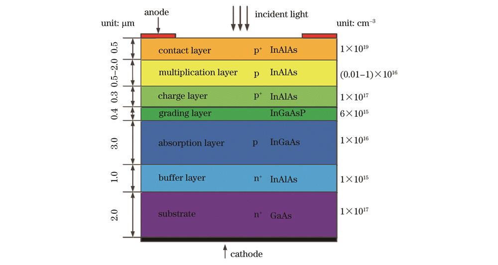
Avalanche photodetectors with inner multiplication gain have greater sensitivity than PIN photodetectors without altering the signal characteristics, which is more suitable for application in optical communication and other related fields. Among them, the separation of absorption, multiplication, and charge layer structure of InGaAs avalanche photodetectors are extensively studied. Through the reasonable design of multiplication layer structure parameters, the high electric field in the multiplication layer and low electric field in the absorption layer can be regulated by the charge layer at the same time, which results in a better multiplication effect in the multiplication layer and inhibits current generated in the absorption layer. In addition, the ternary compound In0.83Al0.17As has higher carrier ionization rate and electron mobility than InP, so it has greater benefits as the multiplication layer for avalanche photodetectors. However, there are few reviews on the effect of the doping concentration and thickness of the multiplication layer on the device performance. To deeply explore the variation rule of avalanche photodetectors in linear mode and elaborate on the impact of the multiplication layer parameters on the device photoelectric performance, this paper studies the doping concentration and thickness of the multiplication layer of In0.83Ga0.17As/GaAs avalanche photodetector in detail. It aims to explore the influence of different doping concentrations and thicknesses of the multiplication layer on the current characteristics, electric field intensity, and capacitance of the device, and research the relationship of the punch-through voltage and breakdown voltage of the device with the doping concentration and thickness of the multiplication layer. It is of great significance to discover the working mechanism of the device in linear mode.
In this study, the effect of the In0.83Al0.17As multiplication layer on the overall performance of In0.83Ga0.17As/GaAs avalanche photodetector is researched with a device simulation tool Silvaco-TCAD. Firstly, the physical models related to conmob, fldmob, auger, srh, bgn, bbt, optr, and impact selb have been applied to define the material parameters of each layer of the device. The energy band and electric field distribution of the device are simulated, which suggests that the device meets the prerequisites of avalanche multiplication and explains the avalanche multiplication process. Secondly, the I-V characteristics of the device in dark and light conditions are simulated. Finally, the effects of the doping concentration and thickness of the multiplication layer on the internal electric field distribution, the punch-through voltage and breakdown voltage, and the traits of the alternating current small signal are simulated. In addition, the combination of electric field distribution and multiplication factor is utilized to explain the variation of punch-through voltage and breakdown voltage.
In this study, the impact of the doping concentration and thickness of the multiplication layer on the electric field intensity, current characteristics, and capacitance characteristics of In0.83Ga0.17As/GaAs avalanche photodetector is explored in detail. The results exhibit that with the thickness of the multiplication layer increasing from 0.5 μm to 2.0 μm, the peak electric field intensity and capacitance decline from 4.9×10⁵ V/cm and 1.4×10⁻¹⁵ F/μm to 4.1×10⁵ V/cm and 0.6×10⁻¹⁵ F/μm, respectively. In addition, the rise in the doping concentration of the multiplication layer causes an increase in the capacitance and the peak electric field intensity in the multiplication layer. When the doping concentration of the multiplication layer is 1×1016 cm-3, the values are 1.4×10⁻¹⁵ F/μm and 5.6×10⁵ V/cm, respectively. Further research shows that with the increment in the thickness of the multiplication layer, the punch-through voltage of the device increases linearly, while the breakdown voltage at the thickness of 0.5 μm, 1.0 μm, 1.5 μm, and 2.0 μm is 50 V, 44 V, 47 V, and 55 V, respectively, which decreases first and then increases. However, a higher doping concentration of the multiplication layer will lead to a lower breakdown voltage of the device. This study is of great significance for the working mechanism of In0.83Ga0.17As/GaAs avalanche photodetector in linear mode and the application of high-speed transmission in the future.