
Shuxin Tan, Takashi Egawa. Influence of growth conditions of oxide on electrical properties of AlGaN/GaN metal–insulator–semiconductor transistors[J]. Journal of Semiconductors, 2019, 40(4): 042801
- Journal of Semiconductors
- Vol. 40, Issue 4, 042801 (2019)
Abstract
1. Introduction
GaN and AlN alloys are good choices for the fabrication of optoelectronics and electronic devices, such as light-emitting diodes, ultraviolet detectors, and high-power and high-frequency electronic devices, due to their excellent material properties[
2. Experimental
The HEMT structure consisted of unintentionally doped-Al0.26Ga0.74N (25 nm)/unintentionally doped-GaN (1 μm)/super lattices (GaN/AlGaN)/buffer layer (AlGaN/AlN) grown by metal organic chemical vapor deposition (MOCVD) on a 4-inch silicon substrate. The fabrication of HEMTs and two-terminal circular diodes for capacitance–voltage (C–V) measurement started with device isolation by BCl3 plasma reactive ion etching. Then silicon oxide was deposited by different deposition techniques and deposition conditions. After etching the silicon oxide with buffered HF solution, the ohmic contact was formed using Ti/Al/Ni/Au (15/72/12/40 nm) followed by rapid thermal annealing at 850 °C for 30 s in a N2 atmosphere. The Ni/Ti/Au (40/20/60 nm) was deposited on silicon oxide as a gate electrode. Several samples have been fabricated in terms of oxide deposition. Oxides for samples A and B were deposited with similar thickness by RF sputter at room temperature (RT) and 150 °C, respectively, under Ar atmosphere. Oxides for samples C and D were deposited by RF sputter at 150 °C under Ar and Ar/O2 atmosphere (Ar : O2 = 1 : 1), respectively. The difference of sample B and sample C was the oxide thickness. Oxide for sample E was deposited by electron-beam evaporation at 150 °C under oxygen atmosphere. Oxides for samples C, D and E have a similar thickness. The target for sputter is silicon oxide. The gate length and width for HEMT devices is 1.5 and 15 μm, respectively. In order to calculate the carrier density and oxide thickness, Schottky diodes without silicon oxide for capacitance–voltage (C–V) measurement were also fabricated. The current–voltage (I–V) characteristics were measured on an Agilent 4156c semiconductor parameter analyzer. Capacitance–voltage (C–V) measurement was carried out using an HP4845 LCR meter.
3. Results and discussion
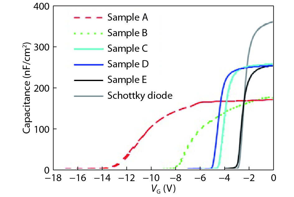
C–V characteristics for all the diodes at 1 MHz are shown in Fig. 1. The thicknesses of silicon oxide films for samples A to E were estimated to be around 11, 10, 3.8, 4.0 and 4.0 nm, respectively, based on the formula,
![]()
Figure 1.(Color online)
where dins is the thickness of silicon oxide, εins is the relative dielectric permittivity of silicon oxide taken as 3.9, εo is the dielectric permittivity of a vacuum, and CMIS and CAlGaN are the unit-area capacitances of the MIS-diodes and the Schottky diode at 0 V, respectively. From C–V curves, the sheet carrier density (ns) could be estimated according to the expression,
where Vth is defined as the gate voltage at which the GaN buffer is depleted in the C–V curve. The ns were calculated to be 1.2 × 10¹³, 6.4 × 10¹², 6.3 × 10¹², 7.0 × 10¹², 3.6 × 10¹² and 5.1 × 1012 cm−2 for samples A to E and Schottky diode, respectively. Considering the very low electron concentration in the GaN buffer compared with the electron density of 2DEG in channel and neglecting the interface states due to high-frequency (HF) capacitance, ns could be regarded as the electron density of 2DEG. It should be noticed that ns in sample A was more than twice of that in the Schottky diode, while sample E reduced 30% compared with the Schottky diode. According to Poisson’s equation and the Schrödinger equation, ns for 2DEG can be expressed as
for Schottky HEMTs, and
for MIS-diode, where
where m* is the electron effective mass of GaN and taken as 0.22m0 (m0 is the free electron mass). Therefore,
Considering
Fig. 2 shows the drain current–drain voltage (ID–VD) curves and transfer characteristics for all the HEMTs. From Figs. 2(a) and 2(b), the drain current density for sample A was larger than that of sample B at the same gate voltage, which was due to larger ns for sample A. The maximum current density (ID-max) for samples A and B were 1323 and 1008 mA/mm, respectively, at the maximum applied gate voltage of 5.5 V. The maximum transconductance (gm-max) for sample A and B were 77 and 90 mS/mm, respectively. The lower gm-max of sample A indicated that the mobility is lower compared with that of sample B, which is possibly because of electron scattering enhancement for sample A due to the highest electron density (exceeded 1013 cm−2 in 2DEG), the remote coulombic scattering enhancement by much more positive interfacial charge and higher sputtered-induced damage in the sputtering process for sample A[
![]()
Figure 2.(Color online) (a) The output characteristics and (b) the transfer characteristics for samples A and B. (c) The output characteristics and (d) the transfer characteristics for samples C, D and E.
Figs. 3(a) and 3(b) showed the drain current–gate voltage (ID–VG) curves and three-terminal gate current density on a semi-logarithmic scale. It can be seen that the off-state gate current density (IG-off) is larger than the off-state drain current density (ID-off), which indicates ID-off is a branch of IG-off for all HEMT devices within the gate voltage sweeping range. Considering the difference of IG-off between the devices is several orders of magnitude and much larger than the difference of ID-max, the ID-on/ID-off ratio mainly depends on IG-off. We compared the IG-off value taken at the turn-around point in a logarithmic ID–VG curve. IG-off on the order of 10 mA/mm for sample A is more than one order of magnitude larger than that of sample B (10−1 mA/mm), which is possibly due to the higher sputter-induced shallow donor-like N vacancies[
![]()
Figure 3.(Color online) The
4. Conclusions
In this paper, AlGaN/GaN based MIS-HEMTs were fabricated using EB-evaporated and sputtered silicon oxide as dielectric. It was found that the electrical properties were influenced by oxide deposition techniques and deposit condition. The high ns and high drain current density as well as high gate leakage could be achieved using silicon oxide as the gate dielectric by RF-sputtering deposition at room temperature, while low ns, positive shift of Vth and low gate leakage could be obtained using EB-evaporated oxide as the gate dielectric. That is, there is a tradeoff among the deposition methods and deposition conditions for the HEMT devices to achieve appropriate electrical properities.
Acknowledgements
This work was partly supported by the National Science Foundation of China (No. 61504071).
References
[1] A Acharyya. Hot electron transport in wurtzite-GaN: effects of temperature and doping concentration. J Semicond, 39, 072002(2018).
[2] F Liang, D G Zhao, D S Jiang et al. Performance enhancement of the GaN-based laser diode by using an unintentionally doped GaN upper waveguide. Jpn J Appl Phys, 57, 070307(2018).
[3] X Huang, C Du, Y Zhou et al. Piezo-phototronic effect in a quantum well structure. ACS Nano, 10, 5145(2016).
[4] X Li, P Ma, X Ji et al. Implementation of slow and smooth etching of GaN by inductively coupled plasma. J Semicond, 39, 113002(2018).
[5] A Tzou, K H Chu, I F Lin et al. AlN surface passivation of GaN-based high electron mobility transistors by plasma-enhanced atomic layer deposition. Nanoscale Res Lett, 12, 315(2017).
[6] D Li, X Sun, H Song et al. Realization of a high-performance GaN UV detector by nanoplasmonic enhancement. Adv Mater, 24, 845(2012).
[7] D G Zhao, J J Zhu, Z S Liu et al. Surface morphology of AlN buffer layer and its effect on the GaN growth by metalorganic vapor chemical deposition. Appl Phys Lett, 85, 1499(2004).
[8] S Tan, X Deng, B Zhang et al. Thermal stability of F ion-implant isolated AlGaN/GaN heterostructures. Sci China-Phys Mech Astron, 61, 127311(2018).
[9] S X Zhao, X Y Liu, L Q Zhang et al. Impacts of thermal atomic layer-deposited AlN passivation layer on GaN-on-Si high electron mobility transistors. Nanoscale Res Lett, 11, 137(2016).
[10] G Meneghesso, M Meneghini, D Bisi et al. Trapping and reliability issues in GaN-based MIS HEMTs with partially recessed gate. Microelectron Reliab, 58, 151(2016).
[11] P Lagger, P Steinschifter, M Reiner et al. Role of the dielectric for the charging dynamics of the dielectric/barrier interface in AlGaN/GaN based metal-insulator semiconductor structures under forward gate bias stress. Appl Phys Lett, 105, 033512(2014).
[12] S Sugiura, S Kishimoto, T Mizutani et al. Normally-off AlGaN/GaN MOSFETs with HfO2 gate oxide. Phys Stat Sol C, 5, 1923(2008).
[13] T Hashizume, S Anantathanasarn, N Negoro et al. Al2O3 insulated-gate structure for AlGaN/GaN heterostructure field effect transistors having thin AlGaN barrier layers. Jpn J Appl Phys, 43, L777(2004).
[14] M Van Hove, X Kang, S Stoffels et al. Fabrication and performance of Au-free AlGaN/GaN-on-silicon power devices with Al2O3 and Si3N4/Al2O3 gate dielectrics. IEEE Trans Electron Devices, 60, 3071(2013).
[15] T Liu, C Jiang, X Huang et al. Electrical transportation and piezotronic-effect modulation in AlGaN/GaN MOS HEMTs and unpassivated HEMTs. Nano Energy, 39, 53(2017).
[16] H Y Shih, F C Chu, C Y Lee et al. Atomic layer deposition of gallium oxide films as gate dielectrics in AlGaN/GaN metal–oxide–semiconductor high-electron-mobility transistors. Nanoscale Res Lett, 11, 235(2016).
[17] J Derluyn, S Boeykens, K Cheng et al. Improvement of AlGaN GaN high electron mobility transistor structures by in situ deposition of a Si3N4 surface layer. J Appl Phys, 98, 054501(2005).
[18] J P Ao, K Nakatani, K Ohmuro et al. GaN metal–oxide–semiconductor field-effect transistor with tetraethylorthosilicate SiO2 gate insulator on AlGaN/GaN heterostructure. Jpn J Appl Phys, 49, 04DF09(2010).
[19] M Asif Khan, X Hu, A Tarakji et al. AlGaN/GaN metal–oxide–semiconductor heterostructure field-effect transistors on SiC substrates. Appl Phys Lett, 77, 1339(2000).
[20] C Liu, E F Chor, L S Tan. Investigations of HfO2/AlGaN/GaN metal–oxide–semiconductor high electron mobility transistors. Appl Phys Lett, 88, 173504(2006).
[21] S Tan, S L Selvaraj, T Egawa. Metal–organic chemical vapor deposition of quasi-normally-off AlGaN/GaN filed-effect transistors on silicon substrates using low-temperature gown AlN cap layers. Appl Phys Lett, 97, 053502(2010).
[22] N Ronchi, B De Jaeger, M Van Hove et al. Combined plasma-enhanced-atomic-layer-deposition gate dielectric and in situ SiN cap layer for reduced threshold voltage shift and dynamic ON-resistance dispersion of AlGaN/GaN high electron mobility transistors on 200 mm Si substrates. Jpn J Appl Phys, 54, 04DF02(2015).
[23] J G Lee, H S Kim, K S Seo et al. High quality PECVD SiO2 process for recessed MOS-gate of AlGaN/GaN-on-Si metal–oxide–semiconductor heterostructure field-effect transistors. Solid State Electron, 122, 32(2015).
[24] P Fiorenza, G Greco, F Iucolano et al. Slow and fast traps in metal–oxide–semiconductor capacitors fabricated on recessed AlGaN/GaN heterostructures. Appl Phys Lett, 106, 142903(2015).
[25] X Sun, D Li, H Jiang et al. Improved performance of GaN metal–semiconductor–metal ultraviolet detectors by depositing SiO2 nanoparticles on a GaN surface. Appl Phys Lett, 98, 121117(2011).
[26] G Dutta, N Das Gupta, A Das Gupta. Effect of sputtered-Al2O3 layer thickness on the threshold voltage of III-nitride MIS-HEMTs. IEEE Trans Electron Devices, 63, 1450(2016).
[27] T Tuan, D H Kuo. Characteristics of RF reactive sputter-deposited Pt/SiO2/n-InGaN MOS Schottky diodes. Mater Sci Semicon Proc, 30, 314(2015).
[28] C Xirouchaki, R E Palmer. Deposition of size-selected metal clusters generated by magnetron sputtering and gas condensation: a progress review. Phil Trans R Soc Lond A, 362, 117(2004).
[29] N Maeda, M Hiroki, N Watanabe et al. Systematic study of insulator deposition effect (Si3N4, SiO2, AlN, and Al2O3) on electrical properties in AlGaN/GaN heterostructures. Jpn J Appl Phys, 46, 547(2007).
[30] O Ambacher, J Majewski, C Miskys et al. Pyroelectric properties of Al(In)GaN/GaN hetero- and quantum well structures. J Phys: Condens Matter, 14, 3399(2002).
[31] J J Zhu, X H Ma, Y Xie et al. Improved interface and transport properties of AlGaN/GaN MIS-HEMTs with PEALD-grown AlN gate dielectric. IEEE Trans Electron Devices, 62, 512(2015).
[32] O Seok, W Ahn, M K Han et al. Effect of Ga2O3 sputtering power on breakdown voltage of AlGaN/GaN high-electron-mobility transistors. J Vac Sci Tech B, 31, 011203(2013).
[33] S J Chang, C H Lan, J D Hwang et al. Sputtered indium-tin-oxide on p-GaN. J Electrochem Soc, 155, H140(2008).
[34] R Stoklas, D Gregušová, Š Gaži et al. Performance of AlGaN/GaN metal–insulator–semiconductor heterostructure field-effect transistors with AlN gate insulator prepared by reactive magnetron sputtering. J Vac Sci Tech B, 29, 01A809(2011).

Set citation alerts for the article
Please enter your email address
© Copyright 2018-2021 | Chinese Laser Press. All Rights Reserved 沪ICP备15018463号-20