• Journal of Semiconductors
  • Vol. 42, Issue 6, 061801 (2021)
Run Tian1、2, Chao Ma3, Jingmin Wu1、2, Zhiyu Guo1、2, Xiang Yang1, and Zhongchao Fan1、4
Author Affiliations
  • 1Engineering Research Center for Semiconductor Integrated Technology, Institute of Semiconductors, Chinese Academy of Sciences, Beijing 100083, China
  • 2College of Materials Science and Opto-Electronic Technology, University of Chinese Academy of Sciences, Beijing 100049, China
  • 3University of Electronic Science and Technology of China, Chengdu 610054, China
  • 4School of Electronic, Electrical and Communication Engineering, University of Chinese Academy of Sciences, Beijing 100049, China
  • show less
    DOI: 10.1088/1674-4926/42/6/061801 Cite this Article
    Run Tian, Chao Ma, Jingmin Wu, Zhiyu Guo, Xiang Yang, Zhongchao Fan. A review of manufacturing technologies for silicon carbide superjunction devices[J]. Journal of Semiconductors, 2021, 42(6): 061801 Copy Citation Text show less
    (a) A typical P–i–N structure. (b) Electric field distribution.
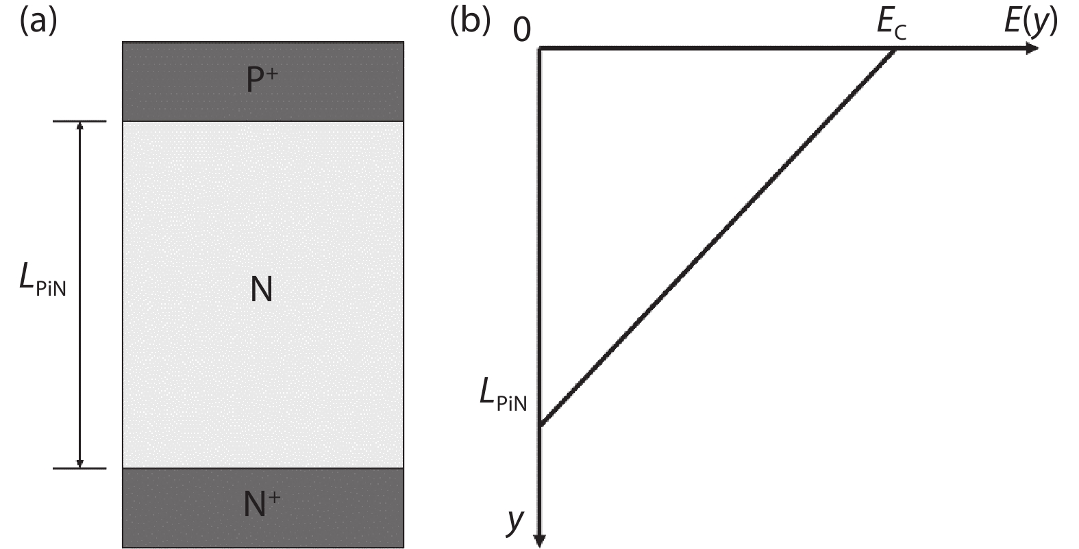
    Fig. 1. (a) A typical P–i–N structure. (b) Electric field distribution.
    (a) SJ structure. (b) Electric field distribution in y- and x-directions.
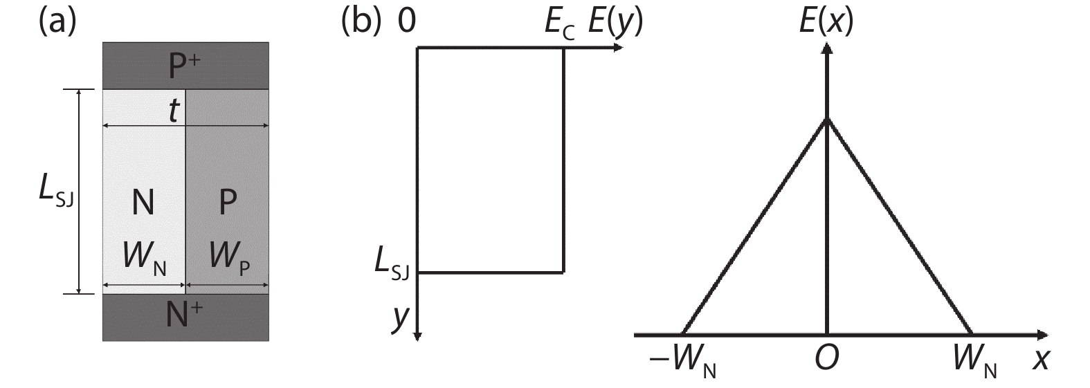
    Fig. 2. (a) SJ structure. (b) Electric field distribution in y- and x-directions.
    Process flow diagram of MEG.
    Fig. 3. Process flow diagram of MEG.
    (Color online) The schematic diagram of energy-filter technology[15].
    Fig. 4. (Color online) The schematic diagram of energy-filter technology[15].
    Process flow diagram of TFE.
    Fig. 5. Process flow diagram of TFE.
    A schematic diagram of trenches parallel to .
    Fig. 6. A schematic diagram of trenches parallel to .
    The schematic diagram of the trench mask pattern.
    Fig. 7. The schematic diagram of the trench mask pattern.
    The schematic diagrams of the cross section of the samples after trench filling.
    Fig. 8. The schematic diagrams of the cross section of the samples after trench filling.
    Process flow of the trench and implantation technique.
    Fig. 9. Process flow of the trench and implantation technique.
    (Color online) The schematic diagram of the trenches with inclined sidewall.
    Fig. 10. (Color online) The schematic diagram of the trenches with inclined sidewall.
    Depth (μm) 135102050
    Ion implantation energy (MeV) N-doping1.15.49.619.435.572.5
    Al-doping1.37.516.338.575.0165.0
    Table 1. The calculation results of SRIM software.
    Run Tian, Chao Ma, Jingmin Wu, Zhiyu Guo, Xiang Yang, Zhongchao Fan. A review of manufacturing technologies for silicon carbide superjunction devices[J]. Journal of Semiconductors, 2021, 42(6): 061801
    Download Citation