
Run Tian, Chao Ma, Jingmin Wu, Zhiyu Guo, Xiang Yang, Zhongchao Fan. A review of manufacturing technologies for silicon carbide superjunction devices[J]. Journal of Semiconductors, 2021, 42(6): 061801
- Journal of Semiconductors
- Vol. 42, Issue 6, 061801 (2021)
Abstract
1. Introduction
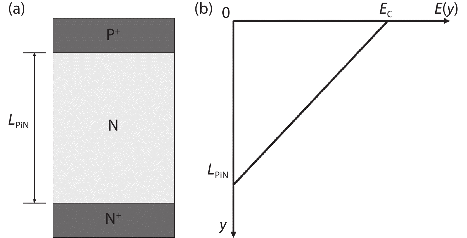
Power semiconductor devices play an important role in electric transmission and power conversions[
![]()
Figure 1.(a) A typical P–i–N structure. (b) Electric field distribution.
where
The solution of Eq. (1) indicates a triangular electric profile across the drift region, as shown in Fig. 1(b)[
where BV is the breakdown voltage and
From Eq. (3), the following relationships can be obtained:
Eq. (4) indicates that power devices made of the substrate material with a higher critical electric field (
According to Eq. (5), for simple P–i–N structures, the
A typical SJ structure consists of alternating n- and p-type columns, as shown in Fig. 2(a). In the SJ structure, the voltage blocking capability is enhanced by the two-dimensional extension of the depletion layers. The electric field distribution in two directions is shown in Fig. 2(b). When the charges in the n- and p-columns are fully compensated, the electric field distribution of the drift region along the y-direction is uniform at a value equal to critical electric field (
![]()
Figure 2.(a) SJ structure. (b) Electric field distribution in
The specific on-resistance for the drift region in the typical SJ device (
Therefore, the relationship between
The
Similar to Si, SJ technology could also be introduced in SiC power devices to improve the BV–
However, due to the extremely stable chemical and physical characteristics of SiC materials, it is difficult to produce an SJ structure. This paper is to summarize recent efforts to pursue SiC SJ devices.
2. Process development
Currently, multi-epitaxial growth (MEG)[
2.1. Multi-epitaxial growth (MEG)
A simplified SiC SJ structure process flow (Fig. 3) of multi-epitaxial growth (MEG) is schematically shown here: a) growing n-epitaxy on an n+ substrate wafer; b) depositing the ion implantation hard mask; c) defining p-type columns by photolithographic and etching processes; d) p-type high energy “box” ion implantation; e) repeating the above cycle of epitaxy and ion implantation process for several times until the desired thickness is achieved; and f) annealing at high temperature to activate the p-type impurities, usually aluminum (Al) ion.
![]()
Figure 3.Process flow diagram of MEG.
There are two advantages of this technology. One is that the doping concentration of n- and p-columns in each layer can be easily controlled[
Most of the MEG approach is to make p-columns on n-type epitaxial layers. The continuous p-columns of Si SJ devices were connected in MEG by diffusion in the thermal budget of the process. However, in SiC, due to the strong chemical bonding, diffusion coefficients of dopants in the high-temperature diffusion are extremely small. For example, the diffusion coefficient of Al atom, a p-type dopant Al+ commonly used in SiC, is only about 10–16 cm2 s–1 at a temperature as high as 1800 °C. Thus, when making SiC SJ structures, it is not practical to connect the implanted p-regions into a continuous p-column by diffusion. Therefore, the diffusion process used in Si technology is not suitable for making SiC SJ structures, and it has to rely on a multiple ion implantation process to produce a “box” doping profile in SiC. In Ref. [13], the research team of the National Institute of Advanced Industrial Science and Technology (AIST) in Japan used seven cycles of epitaxial growth and ion implantation to form an SJ structure of 4.5 μm. In order to make SJ structures with a large depth, the number of cycles is increased accordingly. However, the increase in the number of the cycles brings process challenges, such as the alignment between each step, and the stress between epitaxial layers. These challenges are critical to achieving a deep SJ structure.
Reducing the number of epitaxy-implantation cycles could be achieved by raising ion implantation energy to increase the doping depth of each cycle. In Ref. [14], the AIST research team made a test device with an SJ structure through two-cycle n-type epitaxial growth and high energy p-type ion implantation. Through two ion implantations with maximum energies of 7 and 5.5 MeV, respectively, Al box profiles were formed with depths of 3 and 2.5 μm. As a result, the total depth of the SJ structure was 5.5 μm.
An energy-filter technology developed by MI2-FACTORY in 2019[
![]()
Figure 4.(Color online) The schematic diagram of energy-filter technology[
However, the main challenge of the MEG approach is the limited availability of ultra-high energy implanters (with energy in the MeV scale) for SiC wafers. In order to implant impurities as deep as 5.5 μm, an ultra-high energy above 18 MeV is needed, according to the stopping and range of ions in matter (SRIM) simulation. And to make SJ structures with depths of 10, 20, and 50 μm, the required energy is up to about 38.5, 75, and 165 MeV, respectively. SiC devices are expected to be used in ultra-high voltage applications, for instance, above 10 kV applications. The epitaxial layer thickness will exceed 100 μm. It suggests that extremely high-energy implantation tools are needed to reduce the epitaxy-implantation cycles, even with this new implantation filter technology. But the high-energy implantation process will increase unknown defects in the crystal. Thus, not only the high-energy ion implanter, but also a high-quality hard mask technology has to be developed. Due to these issues, MEG is not an efficient process option to commercialize high-voltage SiC SJ devices.
As discussed previously, existing research on SiC SJ structures through MEG mostly perform p-type ion implantation on n-type epitaxial layers, but high-energy p-type ion implantation has some technical challenges. It might be worth studying the process flow to perform n-type ion implantation on the p-type epitaxial layer. According to the SRIM simulation (Table 1), the ion implantation energies to reach the same doping depths required for nitrogen (N) ion are much lower than those for Al ion in SiC. N ion is an n-type dopant commonly used in SiC ion implantation. However, the epitaxial defects in p-type epitaxial layers is difficult to reduce[
2.2. Trench-filling epitaxial growth (TFE)
The process flow (Fig. 5) of trench-filling epitaxial growth (TFE) is schematically shown here: a) growing n-epitaxy or p-epitaxy on an n+ substrate wafer; b) etching a deep trench on the epitaxial layer; c) filling the trench with p- or n-epitaxy; and d) surface planarization to facilitate subsequent device manufacturing. Most of the research is to etch trenches on n-type epitaxial layers and then fill them with p-type epitaxial layers.
![]()
Figure 5.Process flow diagram of TFE.
As discussed in Section 2.1, due to the limitation of high-energy implantation and diffusion depth, it is not practical to make deep SJ structures by MEG, for example, a 10 μm SJ structure. Ref. [14] processed two epitaxy-implantation cycles and the ion implantation energy up to 7 MeV to produce a 5.5 μm deep SJ. At least four epitaxy-implantation cycles are required to make a 10 μm SJ structure. TFE can simplify the process greatly: etching a 10 μm trench, and growing an epitaxial layer to fill the trench. Thus, as the depth of the SJ structure increases, TFE is more practical to make SJ structures than MEG. However, there are also several technical challenges for TFE.
Firstly, the formation of micron trenches at the bottom corners during etching should be prevented. The formation of micron trenches is a common issue in SiC inductively coupled plasma (ICP) etching process. V-shaped micron trenches at the trench corners are produced when the edge of the trench is etched faster than the center of the trench[
Secondly, it is difficult to grow a flawless single-crystal SiC epitaxial layer to fill the trench. The epitaxial layer will grow from the bottom of the trench, as well as the sidewalls of the trench. However, the bottom and sidewalls of the trench are of different crystal planes. The trench bottom corresponds to
![]()
Figure 6.A schematic diagram of trenches parallel to
Thirdly, a void-free trench filling is a process challenge. There might be two causes to the formation of voids during SiC trench filling. One is that the overgrowth of the epitaxial layer on the mesa top leads to close the trench opening before the trench is completely filled. This can be improved by controlling the epitaxial growth conditions, such as growth temperature, C/Si ratio (ratio of C and Si atoms in supplied source gases), and growth pressure. Due to the large surface diffusion length of reactant species at high temperature (>1600 °C)[
The formation of the voids can also be attributed to the tilt of the epitaxial layer on the mesa top. In Ref. [25], the AIST research team slightly misaligned the trench direction from
![]()
Figure 7.The schematic diagram of the trench mask pattern.
![]()
Figure 8.The schematic diagrams of the cross section of the samples after trench filling.
Fourthly, the doping profile of the filling region is not uniform. Ref. [26] evaluated the doping profile of the p-region by a scanning spreading resistance microscopy (SSRM). The SSRM result showed a lower concentration at the trench sidewalls. Ref. [27] found that the doping profile in the filling region of trenches without micron trenches is relatively uniform. Thus, it seems that the lower concentration at the trench sidewall might be attributed to the formation of the micron trenches at the trench corners. However, the mechanism of forming such a doping profile is still under research.
Furthermore, even a p-type epitaxial layer grown on a planar substrate still has a problem of high density of epitaxial defects[
2.3. Trench and implantation technique
As discussed previously, both MEG and TFE approaches have to overcome some technical challenges to make a functional SJ device. The research team in Zhejiang University proposed a compromise process: a combination of the trench etching and implantation technique to realize a SiC SJ structure[
The process flow (Fig. 9) is schematically shown here: a) growing n-epitaxy on an n+ substrate wafer; b) etching trench with a taper angle intentionally; c) implanting straightly and then at an angle to form a p-region surrounding the trench; d) annealing at high temperature to activate the p-type dopants; e) refilling the trench by SiO2. The p-type region surrounding the trench is performing as the p-columns in the standard SJ structures.
![]()
Figure 9.Process flow of the trench and implantation technique.
It is worth noting that the trench sidewall has a certain inclination. The tapered trenches favor the tilted ion implantation. However, it does not help to form a uniform implantation profile on the sidewall as the depth of the trench increasing. The schematic diagram of the trenches with an inclined sidewall is shown in Fig. 10. The three trenches shown in Fig. 10 have different depths. As the trench depth increases, the trench opening should be narrowed accordingly to reduce the cell pitch of the SJ structure, and then the slope of the sidewall would become more vertical (
![]()
Figure 10.(Color online) The schematic diagram of the trenches with inclined sidewall.
As discussed previously, SiC SJ structures are expected to be used in ultra-high voltage applications, which require a large SJ structure depth. Due to the limitation in the depth of SJ structures made by the combination of trench etching and implantation, this technology is not a feasible approach for producing SiC SJ structures in the industry.
3. Conclusion
The application of SiC SJ structure can improve the trade-off relationship between
Most MEG and TFE approaches perform p-type ion implantation or p-type epitaxy on an n-type epitaxial layer, though many technical challenges need to be solved in the future. Because the technical challenge of n-type ion implantation or epitaxy of SiC is less than that of p-type, it is worth studying to make SiC SJ structure by performing n-type ion implantation or epitaxial trench-filling on the p-type epitaxial layer. Therefore, it is expected to find out the works on the either p-epitaxy based MEG and TFE efforts on SiC SJ process studies in the future.
Acknowledgements
This work was supported by the National Key Research and Development Program (No. 2016YFB0400500), and the Key Research and Development Projects in Guangdong Province (No. 2019B010144001).
References
[1] B J Baliga. Trends in power semiconductor devices. IEEE Trans Electron Devices, 43, 1717(1996).
[2] A Q Huang. Power semiconductor devices for smart grid and renewable energy systems. J Proc IEEE, 105, 2019(2017).
[3]
[4]
[5] H Tsuchida, I Kamata, T Jikimoto et al. Epitaxial growth of thick 4H-SiC layers in a vertical radiant-heating reactor. J Cryst Growth, 237–239, 1206(2002).
[6] Y Onishi, S Iwamoto, T Sato et al. 24 mΩ·cm2 680 V silicon superjunction MOSFET. International Symposium on Power Semiconductor Devices and ICs, 241(2002).
[7] W Saito, I Omura, S Aida et al. A 20 mΩ·cm2 600 V-class Superjunction MOSFET. International Symposium on Power Semiconductor Devices and ICs, 459(2004).
[8] M Rub, M Bar, G Deboy et al. 550 V superjunction 3.9 Ω·mm2 transistor formed by 25 MeV masked boron implantation. International Symposium on Power Semiconductor Devices and ICs, 455(2004).
[9]
[10] S Iwamoto, K Takahashi, H Kuribayashi et al. Above 500 V class Superjunction MOSFETs fabricated by deep trench etching and epitaxial growth. International Symposium on Power Semiconductor Devices and ICs, 31(2005).
[11] J Sakakibara, Y Noda, T Shibata et al. 600 V-class super junction MOSFET with high aspect ratio P/N columns structure. International Symposium on Power Semiconductor Devices and ICs, 299(2008).
[12] F Udrea, G Deboy, T Fujihira. Superjunction power devices, history, development, and future prospects. IEEE Trans Electron Devices, 64, 713(2017).
[13] Y Kobayashi, S Kyogoku, T Morimoto et al. High-temperature performance of 1.2 kV-class SiC super junction MOSFET. International Symposium on Power Semiconductor Devices and ICs, 31(2019).
[14] R Kosugi, Y Sakuma, K Kojima et al. First experimental demonstration of SiC super-junction (SJ) structure by multi-epitaxial growth method. International Symposium on Power Semiconductor Devices and ICs, 346(2014).
[15] M Rueb. Addressing production of SiC super-junction MOSFETs. J Compd Semicond, 25, 38(2019).
[16] N Ishibashi, K Fukada, A Bandoh et al. High-quality 100/150 mm p-type 4H-SiC epitaxial wafer for high-voltage bipolar devices. Mater Sci Forum, 897, 55(2017).
[17] R X Ding, Y T Yang, n R Han. Microtrenching effect of SiC ICP etching in SF6/O2 plasma. J Semicond, 30, 016001(2009).
[18] C Han, Y Zhang, Q Song et al. An improved ICP etching for mesa-terminated 4H-SiC P –i –N diodes. IEEE Trans Electron Devices, 62, 1223(2015).
[19] G M Beheim, L J Evans. Control of trenching and surface roughness in deep reactive ion etched 4H and 6H SiC. MRS Proc, 911, 0911(2006).
[20] T Kimoto, T Yamamoto, Z Y Chen et al. 4H-SiC (11-20) epitaxial growth. Mater Sci Forum, 338–342, 189(2000).
[21] Y Takeuchi, M Kataoka, T Kimoto et al. SiC migration enhanced embedded epitaxial (ME3) growth technology. Mater Sci Forum, 527–529, 251(2006).
[22] T Kimoto, H Matsunami. Surface diffusion lengths of adatoms on 6H-SiC{0001} faces in chemical vapor deposition of SiC. J Appl Phys, 78, 3132(1995).
[23] S Ji, K Kojima, R Kosugi et al. Influence of growth pressure on filling 4H-SiC trenches by CVD method. Jpn J Appl Phys, 55, 01AC04(2016).
[24] S Ji, K Kojima, R Kosugi et al. Filling 4H-SiC trench towards selective epitaxial growth by adding HCl to CVD process. Appl Phys Express, 8, 065502(2015).
[25] R Kosugi, S Ji, K Mochizuki et al. Strong impact of slight trench direction misalignment from [11-20] on deep trench filling epitaxy for SiC super-junction devices. Jpn J Appl Phys, 56, 04CR05(2017).
[26] R Kosugi, Y Sakuma, K Kojima et al. Development of SiC super-junction (SJ) device by deep trench-filling epitaxial growth. Mater Sci Forum, 740–742, 785(2013).
[27] K Kojima, A Nagata, S Ito et al. Filling of deep trench by epitaxial SiC growth. Mater Sci Forum, 742, 793(2013).
[28] X Zhong, B Wang, K Sheng. Design and experimental demonstration of 1.35 kV SiC super junction Schottky diode. International Symposium on Power Semiconductor Devices and ICs, 231(2016).


Set citation alerts for the article
Please enter your email address

© Copyright 2018-2021 | Chinese Laser Press. All Rights Reserved 沪ICP备15018463号-20