• Journal of Semiconductors
  • Vol. 40, Issue 12, 122403 (2019)
Buqing Xu1、3, Qiang Wu2, Lisong Dong3, and Yayi Wei1、3
Author Affiliations
  • 1University of Chinese Academy of Sciences, Beijing 100049, China
  • 2Shanghai Integrated Circuit Research & Development Center, Shanghai 201210, China
  • 3Institute of Microelectronics, Chinese Academy of Sciences, Beijing 100029, China
  • show less
    DOI: 10.1088/1674-4926/40/12/122403 Cite this Article
    Buqing Xu, Qiang Wu, Lisong Dong, Yayi Wei. Selection of DBO measurement wavelength for bottom mark asymmetry based on FDTD method[J]. Journal of Semiconductors, 2019, 40(12): 122403 Copy Citation Text show less
    (Color online) Schematic of the difference of + 1 and –1 diffraction order intensities when (a) d = 0, (b) d > 0, (c) d d.
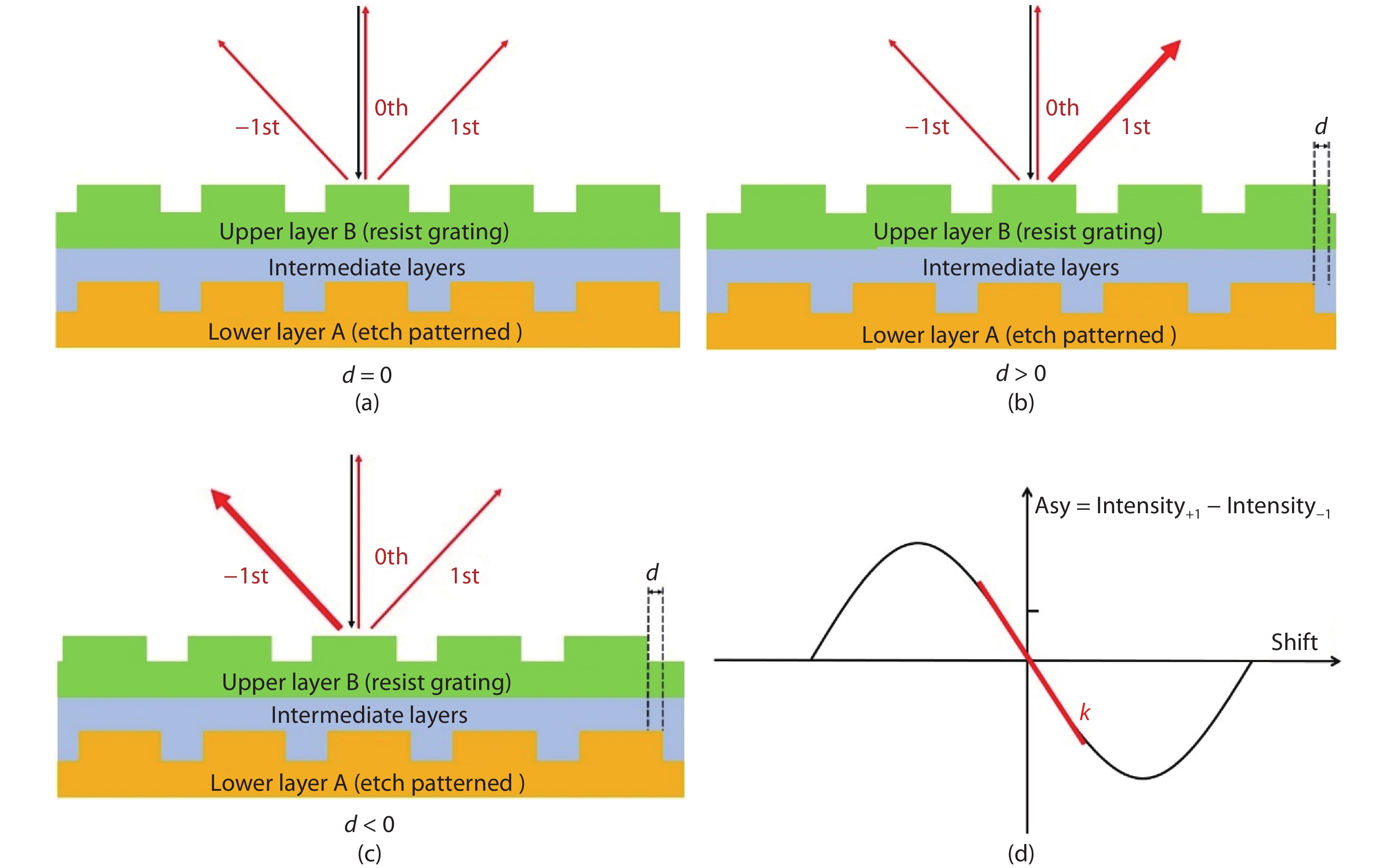
    Fig. 1. (Color online) Schematic of the difference of + 1 and –1 diffraction order intensities when (a) d = 0, (b) d > 0, (c) d < 0. (d) Liner relationship between the difference of intensity and d.
    Schematic of DBO mark. (a) The intentionally introduced bias d ’ in marks. (b) A type of DBO mark that has been widely used.
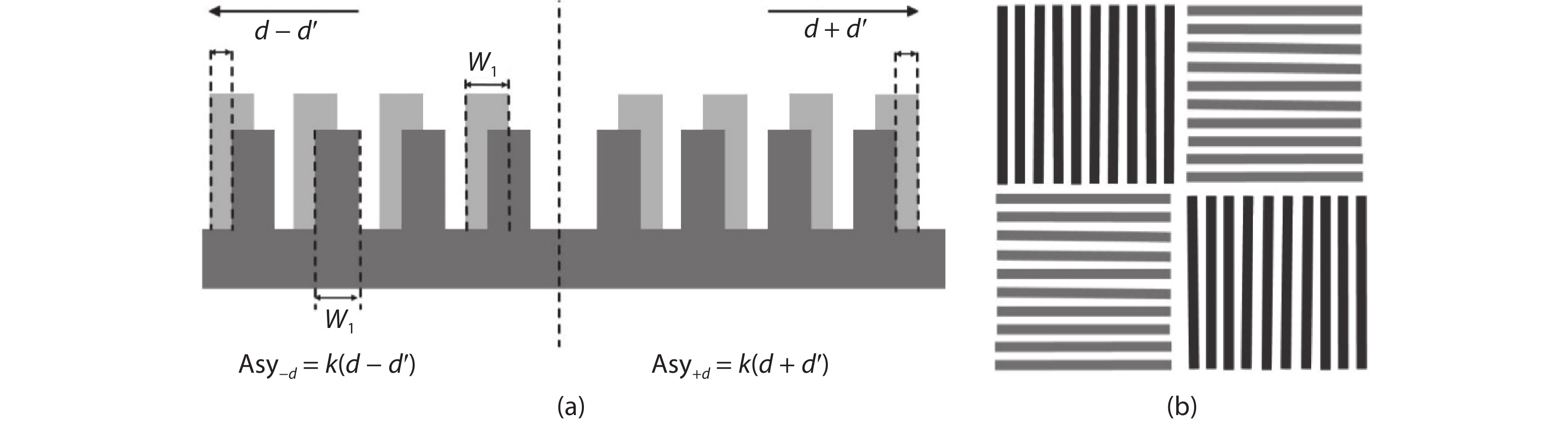
    Fig. 2. Schematic of DBO mark. (a) The intentionally introduced bias d ’ in marks. (b) A type of DBO mark that has been widely used.
    (Color online) (a) Electromagnetic field configuration in Yee cell. (b) Distribution of the electromagnetic component in space.
    Fig. 3. (Color online) (a) Electromagnetic field configuration in Yee cell. (b) Distribution of the electromagnetic component in space.
    (Color online) Schematic of simulation domain in our model.
    Fig. 4. (Color online) Schematic of simulation domain in our model.
    Flow chart of the model (when perform the simulation).
    Fig. 5. Flow chart of the model (when perform the simulation).
    (Color online) A linear relationship between the difference of light intensity and d in a sort of typical film stack can be seen at a fixed wavelength.
    Fig. 6. (Color online) A linear relationship between the difference of light intensity and d in a sort of typical film stack can be seen at a fixed wavelength.
    (Color online) Schematic of overlay marks damaged by CMP: (a) after ideal CMP process, (b) after actual CMP process (mark deformation).
    Fig. 7. (Color online) Schematic of overlay marks damaged by CMP: (a) after ideal CMP process, (b) after actual CMP process (mark deformation).
    (Color online) Schematic of bottom mark asymmetry.
    Fig. 8. (Color online) Schematic of bottom mark asymmetry.
    (Color online) Simulated swing-curves on 4 different film stacks and the wavelength selection preferences.
    Fig. 9. (Color online) Simulated swing-curves on 4 different film stacks and the wavelength selection preferences.
    Electromagnetic field componentSampling of space componentsSampling of the time axis (t)
    x coordinate y coordinate z coordinate
    E node Exi + 1/2 jkn
    Eyij + 1/2 kn
    Ezijk + 1/2 n
    H node Hxij + 1/2 k + 1/2 n + 1/2
    Hyi + 1/2 jk + 1/2 n + 1/2
    Hzi + 1/2 j + 1/2 kn + 1/2
    Table 1. Space coordinates and time steps of E and H components in Yee cell.
    Buqing Xu, Qiang Wu, Lisong Dong, Yayi Wei. Selection of DBO measurement wavelength for bottom mark asymmetry based on FDTD method[J]. Journal of Semiconductors, 2019, 40(12): 122403
    Download Citation