
Buqing Xu, Qiang Wu, Lisong Dong, Yayi Wei. Selection of DBO measurement wavelength for bottom mark asymmetry based on FDTD method[J]. Journal of Semiconductors, 2019, 40(12): 122403
- Journal of Semiconductors
- Vol. 40, Issue 12, 122403 (2019)
Abstract
1. Introduction
As well known that, the critical dimension continues to shrink and the overlay control appears to become much more challenging than before. Faced with such situation, efforts are been made to seek for solutions to minimize the impact of measurement shift in overlay detection induced by process variations. Methods widely used in overlay metrology can be roughly divided into image based overlay (IBO) and diffraction based overlay (DBO). However with the decrease of the overlay budget, it becomes a challenge for IBO to meet the rigid overlay requirement in advanced technology nodes[
DBO has many advantages and is believed to have the potential to become the major technique in overlay measurement. Through the analysis of experiment results, total measurement uncertainty (TMU) of DBO is proved to be in the sub-nanometer range[
In production, however, film stack and size of the overlay mark are diverse on different products and process flows. It will be time-consuming and costly to find the optimal measurement parameters through plenty of experiments without clear direction. In addition, very often the mark deformation caused by process imperfection such as chemical mechanical polishing (CMP) and etch occurs, and it will result in metrology shift in overlay detection. Detectors are unable to distinguish whether the detected asymmetric signal is caused by overlay or resulting from the mark asymmetry induced by process defects[
2. Basis principles for model establishment
2.1. Principle of diffraction-based overlay
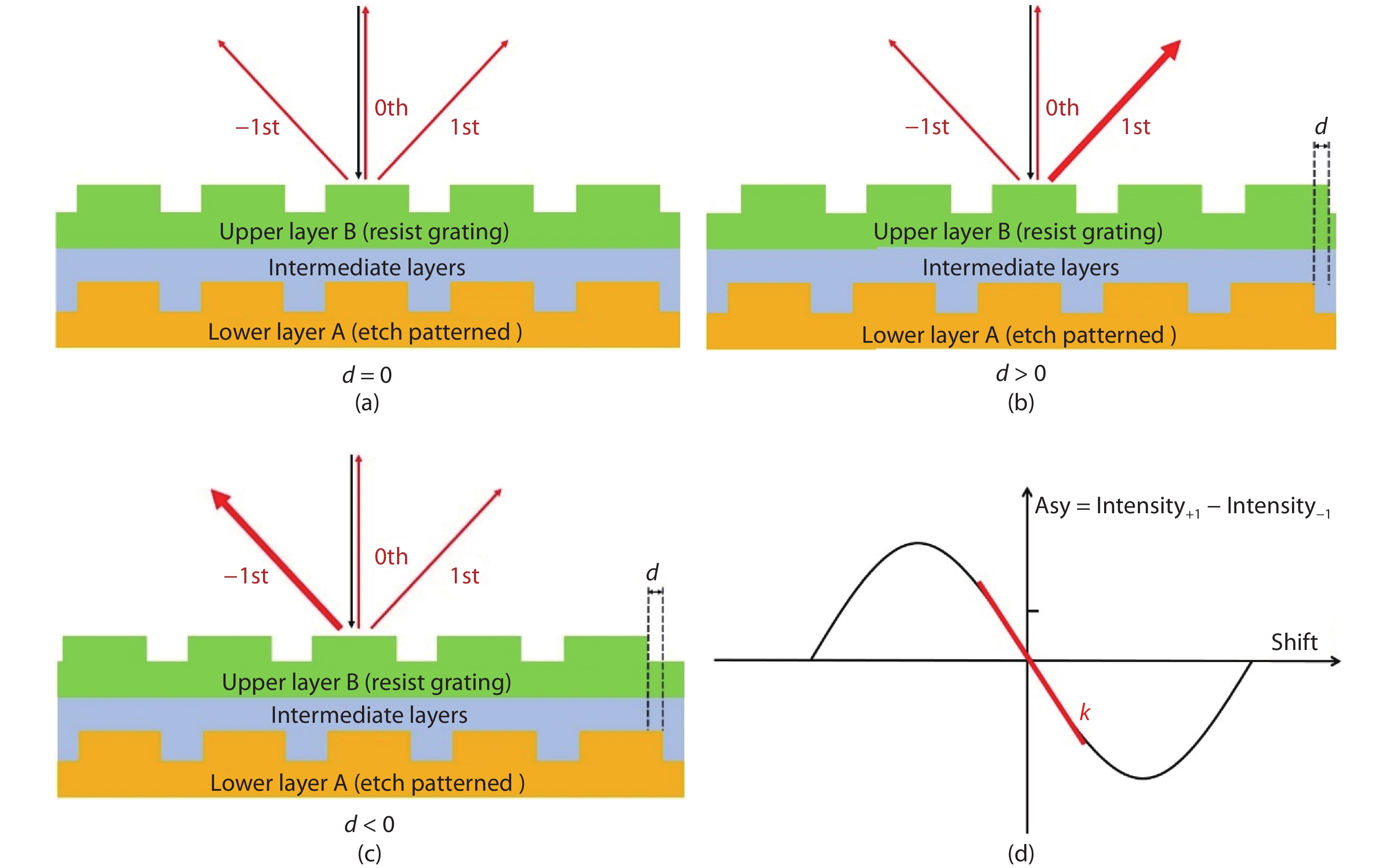
The differences of light intensity are measured and then overlay can be obtained by calculations. When patterns of current layer and reference layer are ideally aligned without shift, that is, the overlay = 0, their overall effect is similar to a reflection grating, and the reflected +/– diffraction order intensities are equal. When overlay exists, conversely, the synthesis effect of the top and bottom marks is asymmetric, and +/– diffraction order intensities are different, as depicted in Fig. 1. Under this circumstance, overlay has a certain relationship with the difference of intensities. It might as well set the intensity of the reflection spectrum be
![]()
Figure 1.(Color online) Schematic of the difference of + 1 and –1 diffraction order intensities when (a)
When overlay is relative small, Eq. (1) can be obtained, which shows the relationship between the intensity of reflection spectrum and the overlay d, as Fig. 1(d) illustrates[
k is a constant related to the structure of film stack and measurement parameters which can be calculated by experiments. It is called overlay sensitivity. What should be noted is that an intentionally bias d ’ need to be applied in order to obtain the linear coefficient k because at least two equations are needed to solve two unknowns, as Fig. 2(a) shows. So, Eq. (2) can be rewritten as:
![]()
Figure 2.Schematic of DBO mark. (a) The intentionally introduced bias
Fig. 2(b) is a typical metrology mark used in DBO, which consists of 1 : 1 dense lines in horizontal direction and 1 : 1 dense lines in vertical direction. Horizontal lines are used to detect the misplacement in y direction and vertical lines for x direction.
2.2. Contents on FDTD involved in model
FDTD solves the Maxwell differential equations rigorously in time domain and is used widely in scattering modeling. In order to discretize the electromagnetic field, alternately sampling E and H (electric field and magnetic field components of the electromagnetic field) in time and space is the key of this method. Every E component is surrounded by four H components, and relatively, every H component is surrounded by four E components. This method was first proposed by Yee and the sampling cube has been called ‘Yee cell’ [
![]()
Figure 3.(Color online) (a) Electromagnetic field configuration in Yee cell. (b) Distribution of the electromagnetic component in space.
Table Infomation Is Not EnableBy means of the division, Maxwell's curl equations are transformed into a group of difference equations and then the result can be obtained by iterating the equations over time. In order to make the calculation as accurate as possible, central difference method is adopted in our model. Such an operation has second-order accuracy, and the introduced error is much smaller than other differential methods[
3. Simulation setup
Through the use of a two-dimensional (2D) FDTD method in the x–z plane, overlay is simulated by vertical illumination in –z direction and a comparison between the reflected + and – diffraction order intensities. In the simulation, a periodical boundary condition in the x direction is adopted, that is, assuming the simulated grating has infinite periods and adopt a second order Mur absorption boundary condition in the top and bottom z boundaries. Parameters involved in the model include pitch of the simulation domain, size of top and bottom marks, refractive index and thickness of each layer. Fig. 4 is a schematic of simulation domain in our model and parameters we use are shown in the figure. Width of the mark refers to that of the single mark line since periodical boundary condition in the horizontal direction is employed.
![]()
Figure 4.(Color online) Schematic of simulation domain in our model.
There are two unknowns need to be solved in the actual measurement environment as revealed in Eqs. (3) and (4), that is, the coefficient or sensitivity k and the d, therefore it is compulsory to set an intentionally bias d ’ in the overlay mark. As a parameter, nevertheless, d is something we set in the model and hence d ’, which is needed in original method, can be skipped in simulations. As far as this difference is concerned, it will not have any impacts on the discussion based on the simulation result that will be carried out below. The grid size in the simulation is 1 × 1 nm2. Besides, when the direction of illumination is from top to bottom, it is stipulated that when the top mark is shifted to the left of the bottom mark, the overlay carries a positive sign, and vice versa. Fig. 5 is the flow chart of the model.
![]()
Figure 5.Flow chart of the model (when perform the simulation).
Simulations based on a typical film structure which is used in manufacturing are performed through this model. The bottom of this mark is silicon substrate, the intermediate layer consists of several oxide layers and other materials, and the top mark is formed by photoresist. The results are shown in Fig. 6. A good linear relationship between the difference of intensity and d at a fixed wavelength can be seen.
![]()
Figure 6.(Color online) A linear relationship between the difference of light intensity and
4. Simulation result and wavelength optimization
Due to the effect of stress and mechanical imperfection, planarization by CMP is not ideal. Specifically, the surface of the bottom overlay mark always have a small slope after polishing, as Fig. 7 depicts and this phenomenon (bottom mark asymmetry) also occurs in process of etch and deposition[
![]()
Figure 7.(Color online) Schematic of overlay marks damaged by CMP: (a) after ideal CMP process, (b) after actual CMP process (mark deformation).
Fig. 8 shows the schematic of bottom mark asymmetry in film stack, which will introduce a small shift (
![]()
Figure 8.(Color online) Schematic of bottom mark asymmetry.
![]()
Figure 9.(Color online) Simulated swing-curves on 4 different film stacks and the wavelength selection preferences.
The wavelength varies from 400 to 800 nm and the difference signal between the +1 and –1 orders are collected, which is linear with k, as a function of wavelength under the fixed overlay condition. Consequently, the swing-curve also can be seen as the result of k along with the change of wavelength. The bands covered by the light box are picked wavelengths that has been optimized. Maximizing k is one of the important criteria that is currently applied in DBO recipe selection.
Although the advantage of DBO lies in the fact that it is not sensitive to the focal distance, therefore robust against metrology equipment variation. But it seems that it lacks ability to isolate overlay signal that is caused by the mark deformation. In contrast, IBO seems to be able to avoid the effect of mark deformation through focus adjustment, i.e., IBO can be optimized to reduce the effect of bottom mark tilt. But the focusing may become quite hard in this case.
5. Conclusion
An FDTD-based overlay measurement model is developed by introducing DBO method and principle involved in the model establishment has been discussed. The model can be utilized to simulate in groups of individual overlay metrology situations and be implemented to find optimized measurement wavelength in DBO. Selection of high k recipes enables DBO measurement be immune to mark asymmetry. Zero-crossing areas in the swing-curve should be avoided for DBO signal formation, where measurement results can be very unstable. In our future work, we will further explore other alternatives to reduce overlay shift induced by the mark deformation.
Acknowledgement
This work was supported by the National Science and Technology Major Project of China (Grant No. 2016ZX02301001).
References
[1] C Simon, C Hsu, Y C Pai et al. Scatterometry or imaging overlay: a comparative study. Proc SPIE, 9424, 942409(2015).
[2] T S Kim, Y S Park, Y C Kim et al. Improved control of multi-layer overlay in advanced 8 nm logic nodes. Proc SPIE, 10585, 1058529(2018).
[3] J Bishoff, R Brunner, J Bauer et al. Light diffraction based overlay measurement. Proc SPIE, 4344, 222(2001).
[4] B Dinu, S Fuchs, U Kramer et al. Overlay control using scatterometry based metrology (SCOM) in production environment. Proc SPIE, 6922, 6922S(2008).
[5] P Leray, D Laidler, S Cheng et al. Achieving optimum diffraction based overlay performance. Proc SPIE, 7638, 76382B(2010).
[6] P Leray, D Laidler, K D'Havé et al. Diffraction based overlay re-assessed. Proc SPIE, 7971, 797114(2011).
[7] W Yang, R Lowe-Webb, Heaton J J. et al. Alignment and overlay metrology using a spectroscopic diffraction method. Advanced Semiconductor Manufacturing Conference and Workshop, 45(2003).
[8] L Zhu, J Li, C S Zhou et al. Overlay mark optimization for thick-film resist overlay metrology. J Semicond, 30, 066002(2009).
[9] P Dasari, N Smith, G Goelzer et al. A comparison of advanced overlay technologies. Proc SPIE, 7638, 76381P(2010).
[10] J Li, Z Liu, Rabello S S. et al. Simultaneous overlay and CD measurement for double patterning: scatterometry and RCWA approach. Proc SPIE, 7272, 727207(2009).
[11] C M Ke, G T Huang, J Huang. Accuracy of diffraction-based and image-based overlay. Proc SPIE, 7971, 79711E(2011).
[12] K Bhattacharyya, A D Boef, M Noot et al. A complete methodology towards accuracy and lot-to-lot robustness in on-product overlay metrology using flexible wavelength selection. Proc SPIE, 10145, 101450A(2017).
[13] S H Oh, J Lee, S Lee et al. The effect of individually-induced processes on image-based overlay and diffraction-based overlay. Proc SPIE, 9050, 905039(2014).
[14] Y Zhou, D Park, K Gutjahr et al. Reducing the overlay metrology sensitivity to perturbations of the measurement stack. Proc SPIE, 10145, 101452G(2017).
[15] K Bhattacharyya, C M Ke, G T Huang et al. On-product overlay enhancement using advanced litho-cluster control based on integrated metrology, ultra-small DBO targets and novel corrections. Proc SPIE, 8681, 868104(2013).
[16] K Bhattacharyya, A D Boef, Storms G G. et al. A study of swing-curve physics in diffraction-based overlay. Proc SPIE, 9778, 97781l(2016).
[17] A D Boef, K Bhattacharyya, M Noot et al. Monitoring accuracy and robustness in on-product diffraction-based overlay metrology. International Conference on Frontiers of Characterization and Metrology for Nanoelectronics, 191(2017).
[18]
[19] K S Yee. Numerical solution of initial boundary value problems involving Maxwell’s equations in isotropic media. IEEE Trans Anten Propag, 14, 302(1966).
[20] A Z Elsherbeni, V Demir. The finite-difference time-domain for electromagnetics with MATLAB simulations. SciTech Publishing, 5(2006).
[21]
[22] R R Liu, Y B Wang, D D Yin et al. A high-efficiency grating coupler between single-mode fiber and silicon-on-insulator waveguide. J Semicond, 38, 054007(2017).
[23] G Mur. Absorbing boundary conditions for finite difference approximation of the time domain electromagnetic field equations. IEEE Trans Electromagn Compat, 23, 377(1981).
[24] M Schaepkens, G S Oehrlein. Asymmetric microtrenching during inductively coupled plasma oxide etching in the presence of a weak magnetic field. Appl Phys Lett, 72, 1293(1998).

Set citation alerts for the article
Please enter your email address
© Copyright 2018-2021 | Chinese Laser Press. All Rights Reserved 沪ICP备15018463号-20