Luying Li, Yongfa Cheng, Zunyu Liu, Shuwen Yan, Li Li, Jianbo Wang, Lei Zhang, Yihua Gao. Study of structure-property relationship of semiconductor nanomaterials by off-axis electron holography[J]. Journal of Semiconductors, 2022, 43(4): 041103
Search by keywords or author
- Journal of Semiconductors
- Vol. 43, Issue 4, 041103 (2022)
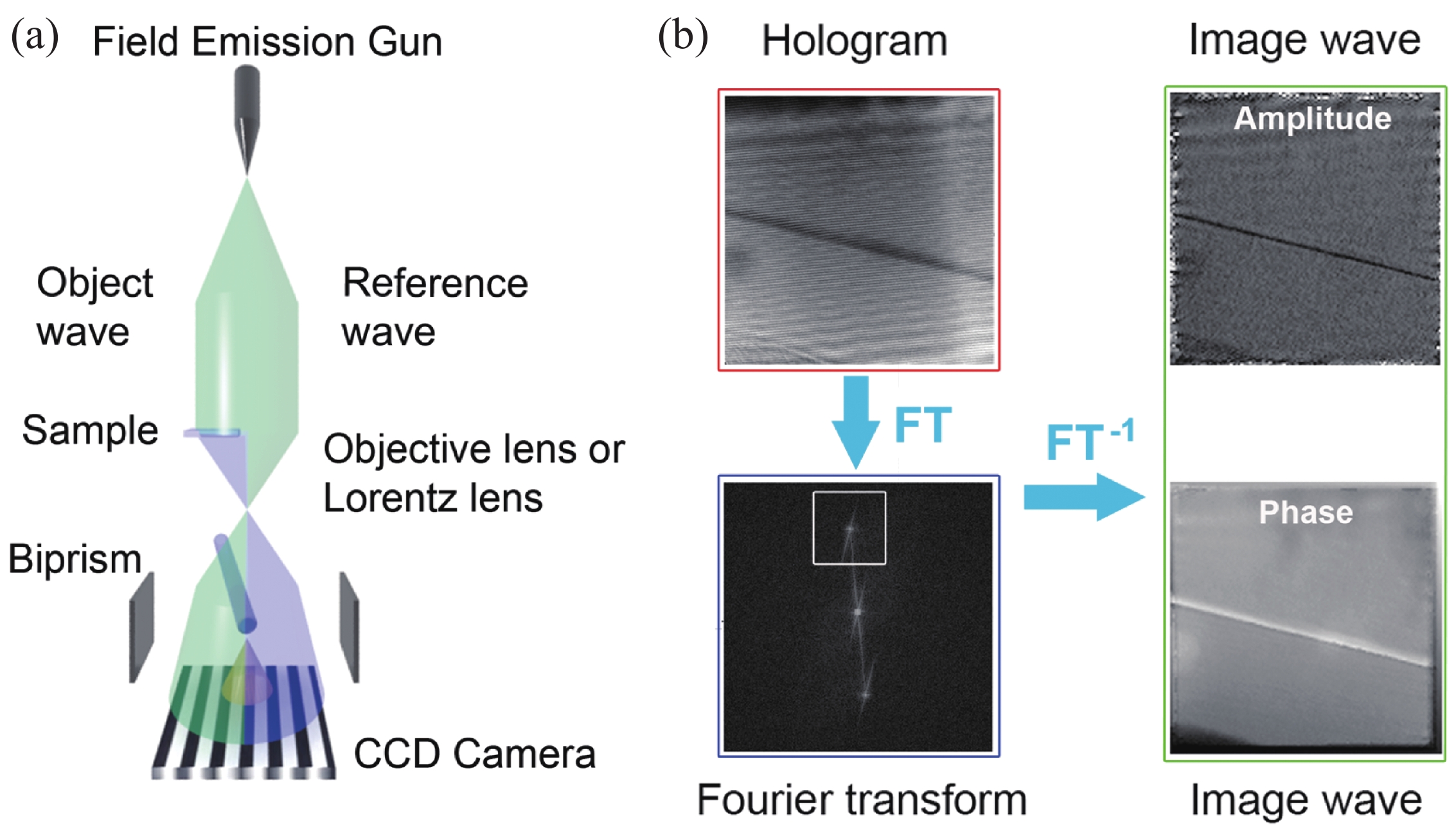
![(Color online) (a) Sketch of off-axis electron holography including three important components: field emission gun, biprism and CCD camera. (b) The reconstruction process of a hologram: The Fourier transform of a hologram produces one center band and two conjugate side bands, one of which is selected and cut out. By applying an inverse Fourier transform, the corresponding amplitude image and phase image can be obtained[8].](/richHtml/jos/2022/43/4/041103/img_1.jpg)
Fig. 1. (Color online) (a) Sketch of off-axis electron holography including three important components: field emission gun, biprism and CCD camera. (b) The reconstruction process of a hologram: The Fourier transform of a hologram produces one center band and two conjugate side bands, one of which is selected and cut out. By applying an inverse Fourier transform, the corresponding amplitude image and phase image can be obtained[8 ].
![(Color online) (a, b) Electron hologram and phase image of specific Ge quantum dot sandwiched in Si substrates. The bottom of Ge dot shows extra positive phase shifts indicating holes accumulated in this region[18]. (c, d) HAADF image of a Ge/Si core/shell nanowire and the corresponding thicknesses of Ge core (blue) and Si shell (red) for the region indicated by a black-dotted arrow in (c). (e, f) Phase image of the same Ge/Si core/shell nanowire and corresponding phase shift line profile across the heterostructures labeled by a black dotted arrow in (e). Extra positive phase shifts appear in the Ge core region indicating hole accumulation in the Ge core[13].](/richHtml/jos/2022/43/4/041103/img_2.jpg)
Fig. 2. (Color online) (a, b) Electron hologram and phase image of specific Ge quantum dot sandwiched in Si substrates. The bottom of Ge dot shows extra positive phase shifts indicating holes accumulated in this region[18 ]. (c, d) HAADF image of a Ge/Si core/shell nanowire and the corresponding thicknesses of Ge core (blue) and Si shell (red) for the region indicated by a black-dotted arrow in (c). (e, f) Phase image of the same Ge/Si core/shell nanowire and corresponding phase shift line profile across the heterostructures labeled by a black dotted arrow in (e). Extra positive phase shifts appear in the Ge core region indicating hole accumulation in the Ge core[13 ].
Fig. 3. (Color online) (a, b) TEM image of an axially biased Si–Ge nanowire heterojunction, and the Ge side is grounded. (b) Electron hologram of the nanowire with +3 V bias on the Si side. (c) Corresponding phase image. (d) Potential line profile of the region indicated by a white arrow in (c), which show abrupt changes at positive bias, and comparatively much less variations at negative bias. (e) Corresponding I–V curve of the same nanowire[19 ]. (f) The sketch of the charge distribution model of the Ge/Lix Ge core/shell structure. (g) Experimental phase shift data (black dots) and the best fitting results based on the above charge distribution model (red dots)[14 ].
Fig. 4. (Color online) (a) Charge distribution profile across InAs QD decorating GaAs NW hetero-interfaces obtained from holographic reconstruction of the phase shifts across the InAs QD/GaAs NW interface. (b) Band structure induced charge redistribution of InAs QDs/GaAs NW heterostructures, which confirms accumulation of electrons at the dot apex and charges of opposite signs distributed at the hetero-interface. (c, d) PL spectra of InAs QDs/GaAs NW (red) and pure GaAs NW (black) for comparison[20 ]. Line profiles of (e) electrostatic potential and (f) charge density across the GaAs/AlGaAs QW/NW heterostructures[21 ].
Fig. 5. (Color online) (a) TEM image of specific straight GaN nanowire connected between two Au electrodes forming a closed electrical circuit. (b) Phase image of the straight GaN nanowire close to the M–S junction. (c) Phase shift line profile of the region labeled by a red line in (b), and the red line indicates average values of the phase shift profile. (d) TEM image of a bent GaN nanowire connected between two Au electrodes. (e) Phase image of the bent GaN nanowire at the M–S junction showing different phase contrasts along radial direction. (f) Phase shift line profiles along the red and green arrows, respectively. The red and green lines represent their average values[25 ].
Fig. 6. (Color online) (a) Potential profiles at –5, –10 and –15 V bias, respectively. The inset shows corresponding phase image. The solid arrow labels the nanowire core for phase profiling, and the two dotted arrows indicate the vacuum regions on either side of the nanowire for phase profiling. (b) 3D calculations of the depletion width W using the Nextnano3 software. The selection of doping level N D = 1018 cm–3 and surface charge density N s = 2.5 × 1012 cm–2 (green triangles) gives the best fit to the experimental depletion widths obtained by electron holography (black diamond)[27 ]. (c, d) Electron holographic phase images of the p–n and p–i–n heterojunctions, respectively. (e, f) The corresponding electrostatic potential profiles of p–n and p–i–n heterojunctions, respectively[28 ].
Fig. 7. (Color online) (a) Electron hologram of MXene-MoS2 2D/2D heterostructure. (b) Corresponding charge density image. (c, d) Charge density line profiles corresponding to the white arrows labeled as (e) and (f), respectively[29 ]. (e) Electron hologram of MoS2/FeS2 heterojunction. (f) Corresponding charge density map and (g) electric field map. (h) Charge density line profile (black) and electric field line profile (red) corresponding to the region labeled by the red dotted arrow in (f) and white dotted arrow in (g), respectively[30 ].

Set citation alerts for the article
Please enter your email address


