• Journal of Semiconductors
  • Vol. 43, Issue 4, 041103 (2022)
Luying Li1, Yongfa Cheng1, Zunyu Liu1, Shuwen Yan1, Li Li1, Jianbo Wang2, Lei Zhang3, and Yihua Gao1
Author Affiliations
  • 1Center for Nanoscale Characterization & Devices, Wuhan National Laboratory for Optoelectronics, Huazhong University of Science and Technology, Wuhan 430074, China
  • 2School of Physics and Technology, Center for Electron Microscopy, MOE Key Laboratory of Artificial Micro- and Nano-Structures, and the Institute for Advanced Studies, Wuhan University, Wuhan 430072, China
  • 3Ministry-of-Education Key Laboratory for the Green Preparation and Application of Functional Materials, Hubei Collaborative Innovation Center for Advanced Organic Chemical Materials, School of Materials Science and Engineering, Hubei University, Wuhan 430062, China
  • show less
    DOI: 10.1088/1674-4926/43/4/041103 Cite this Article
    Luying Li, Yongfa Cheng, Zunyu Liu, Shuwen Yan, Li Li, Jianbo Wang, Lei Zhang, Yihua Gao. Study of structure-property relationship of semiconductor nanomaterials by off-axis electron holography[J]. Journal of Semiconductors, 2022, 43(4): 041103 Copy Citation Text show less

    Abstract

    As the scaling down of semiconductor devices, it would be necessary to discover the structure-property relationship of semiconductor nanomaterials at nanometer scale. In this review, the quantitative characterization technique off-axis electron holography is introduced in details, followed by its applications in various semiconductor nanomaterials including group IV, compound and two-dimensional semiconductor nanostructures in static states as well as under various stimuli. The advantages and disadvantages of off-axis electron holography in material analysis are discussed, the challenges facing in-situ electron holographic study of semiconductor devices at working conditions are presented, and all the possible influencing factors need to be considered to achieve the final goal of fulfilling quantitative characterization of the structure-property relationship of semiconductor devices at their working conditions.
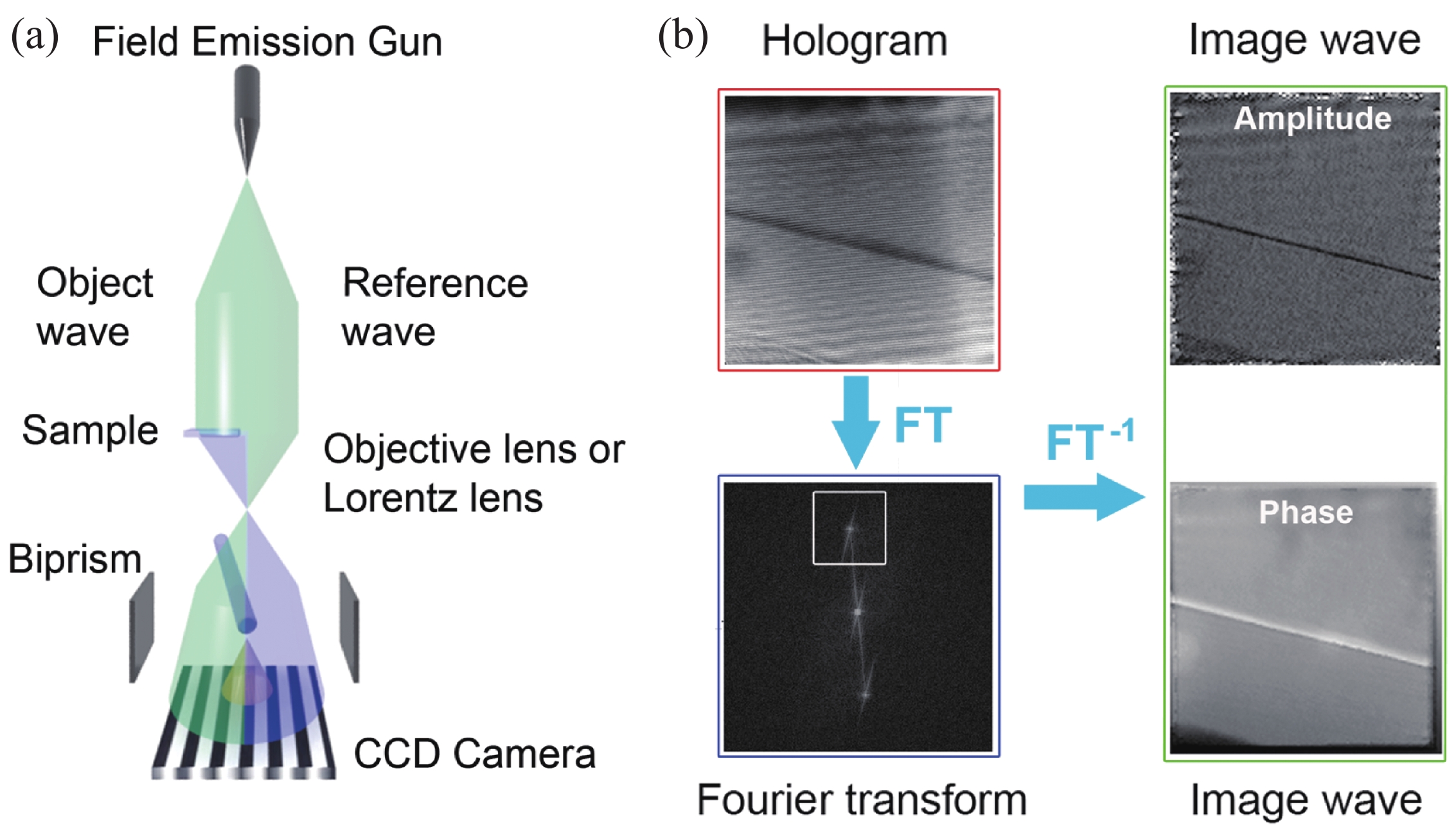
    $ {I_{\rm{complex}}}( \boldsymbol{r} ) = \mu \cdot A( \boldsymbol{r} )\exp (i\phi ( \boldsymbol{r} )) . $ (1)

    View in Article

    $ \rm{phase} = {{\arctan}} (i/r) = \phi ( \boldsymbol{r} ) , $ (2)

    View in Article

    $ \rm{amplitude} = \rm{sqrt}({r^2} + {i^2}) = \mu \cdot A( \boldsymbol{r}) , $ (3)

    View in Article

    $ {\phi} (x) = C_{\rm{E}} \int V(x, z)\rm{d}z , $ (4)

    View in Article

    Luying Li, Yongfa Cheng, Zunyu Liu, Shuwen Yan, Li Li, Jianbo Wang, Lei Zhang, Yihua Gao. Study of structure-property relationship of semiconductor nanomaterials by off-axis electron holography[J]. Journal of Semiconductors, 2022, 43(4): 041103
    Download Citation