• Journal of Semiconductors
  • Vol. 41, Issue 6, 062402 (2020)
Chanrong Jiang, Changchun Chai, Chenxi Han, and Yintang Yang
Author Affiliations
  • School of Microelectronics, Xidian University, Xi’an 710071, China
  • show less
    DOI: 10.1088/1674-4926/41/6/062402 Cite this Article
    Chanrong Jiang, Changchun Chai, Chenxi Han, Yintang Yang. A high performance adaptive on-time controlled valley-current-mode DC–DC buck converter[J]. Journal of Semiconductors, 2020, 41(6): 062402 Copy Citation Text show less
    Schematic of the AOT controlled buck converter.
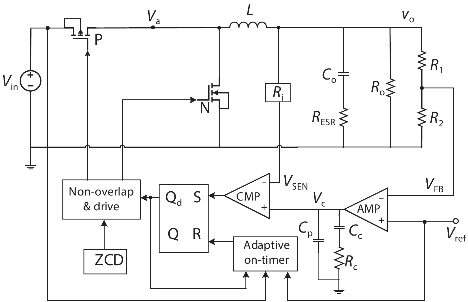
    Fig. 1. Schematic of the AOT controlled buck converter.
    The adaptive on-time controller.
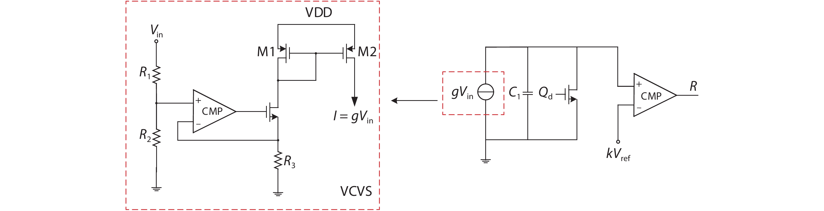
    Fig. 2. The adaptive on-time controller.
    Bode plot of closed loop after compensation.
    Fig. 3. Bode plot of closed loop after compensation.
    Structure diagram of the zero crossing detection module.
    Fig. 4. Structure diagram of the zero crossing detection module.
    The threshold voltage comparator.
    Fig. 5. The threshold voltage comparator.
    (Color online) Simulation results of constant frequency. (a) Varying load current. (b) Varying input voltage. (c) Varying output voltage.
    Fig. 6. (Color online) Simulation results of constant frequency. (a) Varying load current. (b) Varying input voltage. (c) Varying output voltage.
    (Color online) The relationship of Ts between traditional COT and AOT structure proposed in this paper. (a) Variable input voltage. (b) Variable output voltage.
    Fig. 7. (Color online) The relationship of Ts between traditional COT and AOT structure proposed in this paper. (a) Variable input voltage. (b) Variable output voltage.
    (Color online) Simulated load transient response (Vo: 1.2 V, IL: 0.4 →1.2→0.4 A).
    Fig. 8. (Color online) Simulated load transient response (Vo: 1.2 V, IL: 0.4 →1.2→0.4 A).
    (Color online) Output variation curve caused by load current variation.
    Fig. 9. (Color online) Output variation curve caused by load current variation.
    (Color online) Conversion efficiency versus load current at different output voltages.
    Fig. 10. (Color online) Conversion efficiency versus load current at different output voltages.
    Control techniqueInput voltage (V)Output voltage (V)Normalized voltage dropNormalized voltage overshootNormalized setting cycle
    1DPV: digital peak voltage
    Load step variation from 1 to 2 A
    COT-DPV151.50.7800.81
    PWM-DPV51.510.361
    AOT51.50.5800.25
    Load step variation from 2 to 1 A
    COT-DPV51.501.530.826
    PWM-DPV51.50.4311
    AOT51.500.560.188
    Table 1. Comparison results of transient performance between COT, PWM and AOT.
    Control techniquePWM/PFM[1]PWM[26]DLL[27]SAW[28]CTDT[29]This work
    ResultSimulationMeasureMeasureMeasureMeasureSimulation
    Process (μm) 0.350.130.50.350.250.18
    Vin (V) 3.3–51.24.83.355
    Vo (V) 0.5–3.00.6–1.053.30.3–2.51.51.8
    Peak efficiency (%)9082.48388.190.295.5
    Inductor (μH) 500–30000.003–0.0080.11–0.220.222.21.5
    Output capacitor (μF) 50–2000.003730.008–0.192.5620
    fsw (MHz) 0.5–2.1100~30250.51
    Table 2. Comparison results of different control methods.
    ParameterValue
    ProcessStandard 0.18 μm process
    Supply voltage3.3–5.0 V
    Output voltage0.6–3.0 V
    Switching frequency1 MHz
    Load current50–2000 mA
    Inductor1.5 μH
    Output capacitor/ESR20 μF/1 mΩ
    Maximum Efficiency95.5%
    Load regulation rate0.19%/A
    Table 3. Performance summary.
    Chanrong Jiang, Changchun Chai, Chenxi Han, Yintang Yang. A high performance adaptive on-time controlled valley-current-mode DC–DC buck converter[J]. Journal of Semiconductors, 2020, 41(6): 062402
    Download Citation