
Chanrong Jiang, Changchun Chai, Chenxi Han, Yintang Yang. A high performance adaptive on-time controlled valley-current-mode DC–DC buck converter[J]. Journal of Semiconductors, 2020, 41(6): 062402
- Journal of Semiconductors
- Vol. 41, Issue 6, 062402 (2020)
Abstract
1. Introduction
Portable electronic devices such as mobile phones and laptops, are almost completely integrated into every aspect of people’s daily life, which puts higher demands on the performance of the power management systems[
A common method to increase the power efficiency of buck converter is the constant on-time (COT) pulse frequency modulation (PFM) method[
In this paper, an adaptive on time (AOT) valley current mode control scheme is proposed in which the on-time can be adjusted dynamically during CCM and the frequency decreases with the load current under DCM. Constant frequency under CCM can reduce the adverse effects of frequency changes on the output while minimizing the electromagnetic problem simultaneously, which is beneficial to the design of the subsequent filter circuit. For circuit implementation, a simple and accurate zero current circuit is adopted, which allows the converter to switch smoothly between the two conduction modes without the need for an additional mode selection circuit. The rest of the paper is organized as follows. The design of several key modules is presented in Section 2. Simulation results and related analysis are given in Section 3. Finally, the paper is concluded in Section 4.
2. Control strategy and design considerations
2.1. Overall circuit design
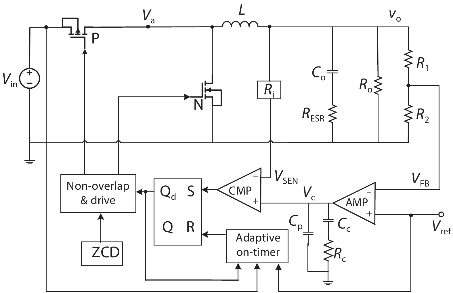
The system block diagram of the proposed adaptive on-time controlled buck converter is illustrated in Fig. 1 which is composed of power stage and feedback control stage. The power stage primarily includes two power transistors for on-off switching and a LC filter, passing the energy from the input to the output[
![]()
Figure 1.Schematic of the AOT controlled buck converter.
The output voltage is divided by resistor R1 and R2 to produce a partial voltage VFB, which is used to compare with a reference voltage Vref. The current sensing circuit detects the current of the freewheeling transistor, and the detected signal VSEN is input to the comparator simultaneously with the output of the error amplifier. When VSEN is lower than Vc, the high level generated by the comparator is fed back to the power stage to turn on the P switch through a series of control modules. At the same time, the N switch is turned off to increase the output voltage until VFB raises to Vref. Then, the next conversion cycle starts. A filter network consisting of capacitor C0 and inductor L produces a steady DC output voltage for DC–DC conversion.
In contrast from the traditional commonly used peak current mode control, this paper uses the valley current mode control and the advantages of the valley current mode are reflected in the following aspects.
(1) A lower duty cycle voltage conversion can be achieved, that is, a large input with a low output. When the duty cycle is reduced, the P switch has a shorter on-time, which put higher requirements on the performance of the conventional current sensing circuit. While the free-wheeling transistor has a longer on-time, so that the current sampling is more convenient.
(2) Better transient response performance. Unlike systems that use peak current mode control, the status of the power transistor which is controlled by the valley current mode is not synchronized with the clock signal, so it can be turned on or off at any time.
2.2. Constant frequency implementation
To eliminate the adverse effects of the varying frequency, parameters related to the switching frequency under CCM is analyzed theoretically:
In the conduction phase of the P switch, the change of inductor current is calculated as follows:
In the off phase of the P switch, the change of the inductor current is as follows:
When the circuit operates under steady state, the increase in inductor current in each cycle is equal to the amount of reduction. Therefore, the switching period can be obtained from Eq. (2) and Eq. (3):
where the quantity, RL, is the equivalent resistance of the inductor. VDSP and VDSN represent the forward voltage drop of the P switch and the N switch, respectively. Since in a well-designed buck converter these parameters are quite small compared to the DC value of Vin and Vo, they can be neglected in the calculation process. The simplified calculation result is as follows:
To keep the switching frequency unchanging in CCM, it is necessary to eliminate the influence of Vin and Vo by adjusting TON. Based on the traditional COT control, an input voltage feedforward control loop and an output voltage feedback loop are introduced. So that TON would vary with changes of input voltage and output voltage. Thereby, the frequency is stabilized at a constant value. The corresponding on-time is as follows:
where gVin represents the value of the voltage controlled current source (VCCS), while kVref represents the value of the voltage controlled voltage source (VCVS). It is implemented by the circuit diagram shown in Fig. 2.
![]()
Figure 2.The adaptive on-time controller.
Since the actual output voltage is a variable with ripple component, if the output voltage is directly used to control the VCVS, the circuit would have stability problems. A reasonable solution is to use the reference voltage Vref instead of the output voltage. When the VCCS (gVin) charges the capacitor C1 to the voltage of the VCVS (kVref), the input terminal of the RS flip-flop, R, will be triggered to high level, which turns the P switch off and turns the N switch on. Upon substituting Eq. (6) into Eq. (5), the final expression of TS can be obtained as follows:
where VO ≈ mVref, and the frequency here is constant without the influence of the input and the output voltage.
2.3. Stability analysis
To analyze the stability of the loop, it is necessary to understand the transfer function of the closed-loop and analyze the impact of the zeros and poles on the system. We then determine whether the compensation network is prerequisite. Ref. [20] gives the categorical modeling method of the open loop for current mode control. In the modeling process, the switches, the inductor, the comparator, and the on-time controller are treated as a single entity, respectively. The describing function method is used to describe the transfer function from the signal Vc to the output signal Vo. The approximate loop gain function of the circuit is given as follows:
where Q1 = 2/π, ω1 = π/TON. It can be seen markly from the transfer function that there are two poles which would cause the instability of the circuit.
To deal with this problem, a compensation network is indispensable for the system design. In this paper, a type Ⅱ compensation network is introduced at the output of the operational amplifier, which is composed of parallel connection of resistor Rc, capacitor Cc and Cp, as shown in Fig. 1. This compensation network introduces two poles, while Rc and Cc are connected in series to produce a left half plane zero. This zero would compensate one pole of the original circuit by adjusting the magnitude of resistor Rc and capacitors Cc, Cp suitably. The gain point is extrapolated to make the feedback system more stable.
The loop-compensated transfer function is simulated in MATLAB and the Bode plot is shown in Fig. 3. The simulation is performed under the conditions of input and output voltage are 5 V and 1.8 V respectively, with the load current of 1 A. It can be seen from the Bode plot that the phase margin of the loop is 57.8 degrees, which satisfies the conditions for stable operation of the system.
![]()
Figure 3.Bode plot of closed loop after compensation.
2.4. Zero current detection
The buck converter discussed in this paper has a reference voltage of 1 V[
![]()
Figure 4.Structure diagram of the zero crossing detection module.
In the discontinuous conduction mode, when the inductor current drops to zero, Va equals to zero, too. Ideally, the moment when Va is equal to zero is taken as the effective time of the ZCD output signal. However, due to the delay time of different circuit modules inside the converter, when Va is equal to zero, it will take a delay time for ZCD to turn off the N switch.
As a result, the inductor current is still reversed during this delay time. Therefore, the value of Va slightly below zero is used as the turning point[
The overall circuit diagram of the threshold voltage comparator is shown in Fig. 5. In practical applications, resistors R3–R6 will be replaced by MOS transistors with constant bias. One of the advantages of this ZCD module, shown in Fig. 4, is that during the half cycle in which the P switch is turned on, that is, during the period in which the inductor current rises, the potential at point X is pulled to zero. As a result, a high level enable signal EN is generated, forcing the output of the threshold voltage comparator to a high level. Consequently, the output of the ZCD module is low during the entire charging process, which avoid a large part of energy loss. When P is high, capacitor C2 is charged by the current source. While the potential of X rises to a certain threshold, the EN is turned to a low level, allowing the comparator to operate normally.
![]()
Figure 5.The threshold voltage comparator.
3. Simulation results
3.1. Switching frequency
From this analysis, the switching frequency should be ideally constant regardless of input voltage, output voltage and load current under CCM. The switching period Ts and on-time Ton of the converter is obtained by the simulation with standard 0.18 μm process, which is shown in Fig. 6. It is obvious from Fig. 6(a) that the switching period can be maintained at a quasi-fixed value over a large load range and the maximum changing rate can be controlled within 4%. Furthermore, the duty cycle is almost changeless as the load current if the input and output voltage are constant.
![]()
Figure 6.(Color online) Simulation results of constant frequency. (a) Varying load current. (b) Varying input voltage. (c) Varying output voltage.
With a constant switching period, because the charge and energy delivered to the output capacitor of each cycle increase as Vin[
Compared with the traditional COT structure, the AOT structure proposed in this paper has better frequency characteristics when the input voltage and output voltage change. Simulation results for the two structures are given in Fig. 7. The output voltage remains constant at 0.6 V when the input voltage changes from 0.8–5.0 V while the input voltage is kept at 5.0 V when the output voltage changes from 0.6–1.8 V. The switching frequency shows to be almost independent on the input voltage and output voltage under AOT control while the switching frequency of COT control varies dramatically with Vin and Vo. As we all know that a constant frequency is more conductive to the design of subsequent filter circuits and contributive to the stability of the whole system.
![]()
Figure 7.(Color online) The relationship of
3.2. Transient performance
The ability for a converter to return to its steady state after the load current changes illustrates the robustness of the circuit[
![]()
Figure 8.(Color online) Simulated load transient response (
The output voltage ripple is composed of capacitor ripple and ESR ripple. So, the total ripple can be expressed as follows:
In CCM, the switching frequency is quasi-constant, so that the amplitude of the output ripple is fixed at a constant value for a given input voltage and output voltage. It can also be seen from Fig. 8 that the magnitude of the output ripple is constant when only the load current changes. This phenomenon has been theoretically verified in Ref. [26].
To better illustrate the transient response characteristics of the AOT structure, comparisons in Table 1 are made to the two structures mentioned in Ref. [24] in voltage drop, voltage overshoot and recovery time. The standard of normalization is the characteristics of PWM structure. Its voltage drop is about 45 mV while the overshoot voltage is about 75 mV with a recovery time of 200 μs. From Table 1, the AOT control has faster transient performance and smaller voltage variation than PWM and COT control under load current steps.
3.3. Load regulation and line regulation
Load regulation rate is one of the ways to measure the performance of a power supply, which would reflect changes in output voltage as a function of load current. Its expression is as follows:
Actually, a change in the output load of the power supply will cause a slight change in the output voltage. For a good power supply, the changes of the output voltage due to load changes are small, typically 3%–5%. In this paper, the load regulation rate is measured under the condition of 1.2 V output voltage with the load current switching from 0.1 to 1 A. The simulation diagram is shown in Fig. 9 and the result is 0.19% after calculation, which is within acceptable limits.
![]()
Figure 9.(Color online) Output variation curve caused by load current variation.
The line regulation of the converter with AOT mode is also obtained as expected. The ripple voltage is higher with a lower load current because the ripple voltage is inversely proportional to the switching frequency.
3.4. Conversion efficiency
The power efficiency is simulated versus the load current and the output voltage as shown in Fig. 10. The peak power efficiency is 95.5% when the load current is 0.95 A and the output voltage is 1.8 V. As can be seen from the figures, the overall trend of the conversion efficiency increases first and then decreases. The load currents corresponding to the broken lines in Fig. 10 indicate that the critical current is related to different output voltages. The crossover losses between the two switches are the main factors of the efficiency losses under light load current conditions which is because the moment when the P switch is turned off, the current flowing through it cannot fall to zero immediately and there is a voltage drop across the P switch, resulting in extra power loss in the case where current and voltage both exist. Meanwhile, there are similar power loss on the N switch.
![]()
Figure 10.(Color online) Conversion efficiency versus load current at different output voltages.
When the load current is reduced to make the converter enter DCM, the conversion efficiency can still maintain a high level over a large load range, especially when the output voltage is higher than 1.8 V. Until the current drops below about 0.1 A, the conversion efficiency drops significantly. The smaller the output voltage, the more obvious the trend. Under extremely light load conditions, the efficiency is greatly reduced due to the increasing proportion of quiescent current. To offset the switching loss, lower switching frequencies are adopted in DCM.
The maximum conversion efficiency under different control methods are further compared in Table 2. The maximum conversion efficiency of AOT can reach 95.5% when the output voltage is 1.8 V. As the output voltage decreasing, the conversion efficiency decreases slightly. The maximum conversion efficiency is about 92% with 0.6 V output voltage. The light load efficiency of the traditional PWM control mode can only reach about 20% while the efficiency of this AOT structure can reach 40% or more. Consequently, the conversion efficiency, especially the conversion efficiency under light load is improved. The performance summary of this design is presented in Table 3.
4. Conclusion
An adaptive-on-time valley current mode controlled buck converter with characteristics of constant frequency in CCM and variable frequencies in DCM is proposed for the application of wide current range and high power efficiency. The proposed converter is designed in standard 0.18 μm process, and composed of power and feedback control stages. First, this circuit can not only solve the problem caused by changing frequency of the traditional COT method but can also improve the conversion efficiency under light load compared with the PWM control mode. Second, it can operate stably under different conduction modes and transform freely without introducing large undershoot voltage and response time. The increase in the allowable output range and effective control of the voltage undershoot make the design of subsequent circuits less difficult. In addition, due to the introduction of variable frequency control in DCM, the overall switching efficiency is greatly improved. Simulation results show that the peak conversion efficiency can reach 95% with 1.8 V output in a large load current range. Besides, the efficiency can be improved as the voltage rises within a certain range, which is more suitable for battery supplied systems.
Acknowledgments
This work was supported by the National Natural Science Foundation of China (No. 61974116).
References
[1] J Yu, I Hwang, N Kim. High performance CMOS integrated PWM/PFM dual-mode DC-DC buck converter. 2017 18th International Scientific Conference on Electric Power Engineering (EPE), 1(2017).
[2] L Wang, F J Lin, Q Cui. Dual 3-phase buck converter for multi-core CPUs power supply in mobile devices. IEICE Electron Express, 14, 20170045(2017).
[3] Y Ma, S Wang, S Zhang et al. A current mode buck/boost DC–DC converter with automatic mode transition and light load efficiency enhancement. IEICE Trans Electron, E98C, 496(2015).
[4] J J Chen, J H Shen, Y S Hwang. High-efficiency fast-transient-response V2-controlled boost converter with small ESR capacitor. Electron Lett, 49, 1402(2013).
[5] X Ke, J Sankman, D Ma. AO2T current mode buck converter with one-cycle transient response and sensorless current detection for medical meters. IEEE Applied Power Electronics Conference and Exposition (APEC)(2016).
[6] X Chen, G Zhou, K Zhang et al. Improved constant on-time controlled buck converter with high output-regulation accuracy. Electron Lett, 51, 359(2015).
[7] Y Yan, F C Lee, P Mattavelli et al. I2 average current mode control for switching converters. 2013 IEEE Applied Power Electronics Conference and Exposition - APEC(2013).
[8] J J Chen, Y S Hwang, J H Chen et al. A new fast-response current-mode buck converter with improved I2-controlled techniques. IEEE Trans Very Large Scale Integr (VLSI) Syst, 26, 903(2018).
[9] R Redl, J Sun. Ripple-based control of switching regulators-an overview. IEEE Trans Power Electron, 24, 2669(2010).
[10] C F Lee, P K T Mok. A monolithic current-mode CMOS DC-DC converter with on-chip current-sensing technique. IEEE J Solid-State Circuits, 39, 3(2004).
[11] B Sahu, G A Rincn-Mora. An accurate, low-voltage, CMOS switching power supply with adaptive on-time pulse-frequency modulation (PFM) control. IEEE Trans Circuits Syst I, 54, 312(2007).
[12] H Nam, Y Ahn, J Roh. A buck converter with adaptive on-time PFM control and adjustable output voltage. Analog Integr Circuits Signal Process, 71, 327(2012).
[13] Y Qiu, H Liu, X Chen. Digital average current-mode control of PWM DC–DC converters without current sensors. IEEE Trans Ind Electron, 57, 1670(2010).
[14] A Barrado, R Vazquez, A Lazaro et al. Fast transient response with combined linear-non-linear control applied to buck converters. IEEE Power Electronics Specialists Conference(2002).
[15] M C Lee, X Jing, P K T Mok. A 14V-output adaptive-off-time boost converter with quasi-fixed-frequency in full loading range. IEEE International Symposium of Circuits and Systems (ISCAS)(2011).
[16] X Jing, P K T Mok, M C Lee. Current-slope-controlled adaptive-on-time DC-DC converter with fixed frequency and fast transient response. IEEE International Symposium on Circuits & Systems(2011).
[17] Y Xu, J Xu, L Xu et al. Constant frequency turn-on time control dynamic voltage scaling boost converter. International Conference on Communications(2013).
[18] X Jing, P K T Mok. A fast fixed-frequency adaptive-on-time boost converter with light load efficiency enhancement and predictable noise spectrum. IEEE J Solid-State Circuits, 48, 2442(2013).
[19] Q Li, X Lai, L Zhong. Adaptive current-threshold detector for an adaptive on-time buck converter at light load. Analog Integr Circuits Signal Process, 95, 541(2018).
[20] J Li, F C Lee. New modeling approach and equivalent circuit representation for current-mode control. IEEE Trans Power Electron, 25, 1218(2010).
[21] H Shi, Z Sun, Y Xu et al. Design of the 1.0 V bandgap reference on chip. IEEE International Conference on ASIC(2016).
[22] S P Huang, Q Y Feng, S J University. Design of a novel zero-cross detection circuit for synchronous buck converter. Chin J Electron Devices, 37, 408(2014).
[23] B Yuan, X Q Lai, H Y Wang et al. High-efficient hybrid buck converter with switch-on-demand modulation and switch size control for wide-load low-ripple applications. IEEE Trans Microwave Theory Tech, 61, 3329(2013).
[24] Y Y Jin, J P Xu, G H Zhou. Constant on-time digital peak voltage control for buck converter. Energy Conversion Congress & Exposition, 2030(2010).
[25] M Gildersleeve, H P Forghanizadeh, S Member et al. A comprehensive power analysis and a highly efficient, mode-hopping DC–DC converter. IEEE Asia-pacific Conference on ASIC(2002).
[26] C Huang, P K T Mok. A 100 MHz 82.4% efficiency package-bondwire based four-phase fully-integrated buck converter with flying capacitor for area reduction. IEEE J Solid-State Circuits, 48, 2977(2013).
[27] P Li, L Xue, P Hazucha et al. A delay-locked loop synchronization scheme for high-frequency multiphase hysteretic DC–DC converters. IEEE J Solid-State Circuits, 44, 3131(2009).
[28] B Lee, M K Song, A Maity et al. 10.7 A 25 MHz 4-phase SAW hysteretic DC–DC converter with 1-cycle APC achieving 190 ns tsettle to 4 A load transient and above 80% efficiency in 96.7% of the power range. Solid-State Circuits Conference(2017).
[29] C K Teh, A Suzuki, M Yamada et al. 4.1 A 3-phase digitally controlled DC-DC converter with 88% ripple reduced 1-cycle phase adding/dropping scheme and 28% power saving CT/DT hybrid current control. IEEE International Solid-State Circuits Conference Digest of Technical Papers(2014).

Set citation alerts for the article
Please enter your email address
© Copyright 2018-2021 | Chinese Laser Press. All Rights Reserved 沪ICP备15018463号-20