Yuan Yuan, Bassem Tossoun, Zhihong Huang, Xiaoge Zeng, Geza Kurczveil, Marco Fiorentino, Di Liang, Raymond G. Beausoleil. Avalanche photodiodes on silicon photonics[J]. Journal of Semiconductors, 2022, 43(2): 021301
Search by keywords or author
- Journal of Semiconductors
- Vol. 43, Issue 2, 021301 (2022)
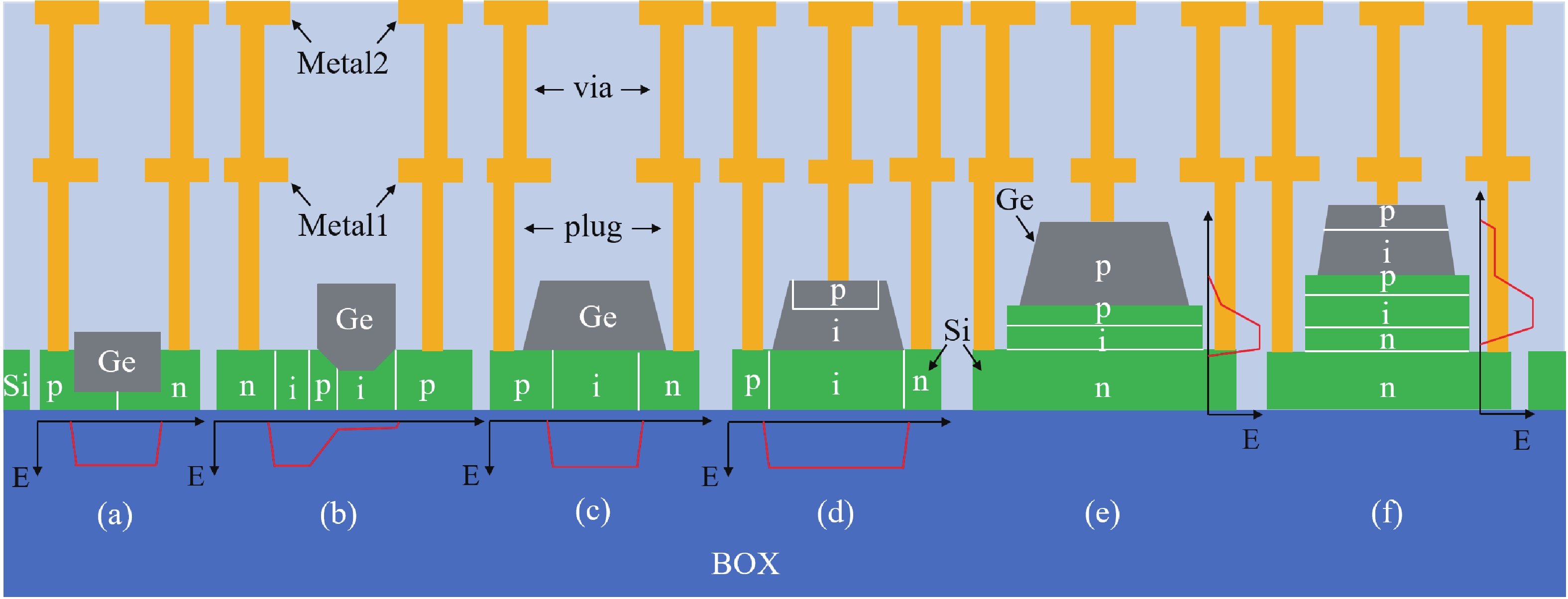
![(Color online) Common structures of Si–Ge APDs with E-field: (a) lateral p–i–n Si–Ge–Si APD[18], (b) Ge on lateral SACM Si APD[19], (c) Ge on lateral p–i–n Si APD[20], (d) hybrid vertical and lateral p–i–n APD[21], (e) vertical SACM p–p–i–n APD[22], and (f) vertical SACM p–i–p–i–n APD[23, 24].](/richHtml/jos/2022/43/2/021301/img_1.jpg)
Fig. 1. (Color online) Common structures of Si–Ge APDs with E-field: (a) lateral p–i–n Si–Ge–Si APD[18 ], (b) Ge on lateral SACM Si APD[19 ], (c) Ge on lateral p–i–n Si APD[20 ], (d) hybrid vertical and lateral p–i–n APD[21 ], (e) vertical SACM p–p–i–n APD[22 ], and (f) vertical SACM p–i–p–i–n APD[23 , 24 ].
![(Color online) I–V curves and eye diagrams of (a) lateral p–i–n Si–Ge-Si APD[18], (b) Ge on lateral SACM Si APD[19], (c) Ge on lateral p–i–n Si APD[20], and (d) hybrid vertical and lateral p–i–n APD[21].](/richHtml/jos/2022/43/2/021301/img_2.jpg)
Fig. 2. (Color online) I –V curves and eye diagrams of (a) lateral p–i–n Si–Ge-Si APD[18 ], (b) Ge on lateral SACM Si APD[19 ], (c) Ge on lateral p–i–n Si APD[20 ], and (d) hybrid vertical and lateral p–i–n APD[21 ].
Fig. 3. (Color online) (a) A cross-sectional structure, (b) a simulated E-field distribution, (c) a gain vs bandwidth plot, temperature-dependent characteristics of (d) gain and breakdown voltage, (e) bandwidth, and (f) 32 Gb/s NRZ and 64 Gb/s PAM4 eye diagrams of the 4 × 10 µ m2 Si–Ge SACM APD[22 , 28 , 31 ].
Fig. 4. (Color online) (a) Schematic of the Si–Ge APD with no reflector (Normal), a distributed Bragg reflector (DBR), and a loop reflector (LR), and (b) simulated absorption profiles. Comparison of (c) reflectivity, (d) photocurrent versus input power at unity gain point (e) impulse responses at gain ~ 10, 32 Gb/s NRZ bit error rate at bias voltage of (f) –8 V and (g) –10 V between the Normal, DBR1, DBR2, and LR APDs. (h) 40 Gb/s NRZ and 80 Gb/s PAM4 eye diagrams of the LR APD at bias of –10 V[32 , 33 ].
Fig. 5. (Color online) Cross-sectional schematic of the InGaAs/InAlAs SACM APD directly on the InP/Si template[52 ].
Fig. 6. (Color online) (a) I–V and gain curves, (b) photocurrent versus input laser power at unity gain point, and (c) excess noise of the 20 µ m-diameter InGaAs/InAlAs APD on Si. Temperature-dependent dark current versus bias voltage of the (d) 20 µ m-diameter APD on Si and (e) 50 µ m-diameter APD on InP. (f) Activation energies at –5 V for APDs on Si and InP[52 ].
Fig. 7. (Color online) (a) Cross-section schematic of the photodiode. (b) SEM cross section of the QD waveguide PD on Si[59 ].
Fig. 8. (Color online) (a) Dark current vs. temperature for a 11 × 60 µ m2 APD. (b) Spectral response versus voltage of a 11 × 90 µ m2 APD. (c) Gain with quasi-TE mode and quasi-TM mode coupled into a 12 × 150 µ m2 APD. (d) Output frequency response of a 3 × 30 µ m2 APD measured with TE and TM modes at –15, –16 and –17 V bias voltage (dashed lines are averaged data). (e) Eye diagram of a 3 × 30 µ m2 APD with a gain of 46.8 at 25 Gb/s. (f) Bit error rate vs. input optical power of an 11 × 90 µ m2 APD at a gain of 28 at 10 Gbit/s[59 ].
Fig. 9. (Color online) (a) Schematic of wafer structure. (b) TEM image of the wafer[67 ].
Fig. 10. (Color online) (a) Schematic plot of the PD fabricated on the GoVS template. (b) Top-view and (c) cross-sectional view SEM images of a fabricated device[68 ].
Fig. 11. (Color online) (a) Schematic diagram of the InAs QD APD grown on GoVS substrate. (b) APD gain versus the reverse bias at various temperatures. (c) Small-signal frequency response of the 3 × 50 µ m2 device for various bias voltages. (d) Measured eye diagrams at a bias voltage of –15.9 V for data rates of 2.5, 5, and 8 Gb/s[69 ].
|
Table 1. Properties of integrated APDs on silicon.

Set citation alerts for the article
Please enter your email address


