
Yuan Yuan, Bassem Tossoun, Zhihong Huang, Xiaoge Zeng, Geza Kurczveil, Marco Fiorentino, Di Liang, Raymond G. Beausoleil. Avalanche photodiodes on silicon photonics[J]. Journal of Semiconductors, 2022, 43(2): 021301
- Journal of Semiconductors
- Vol. 43, Issue 2, 021301 (2022)
Abstract
1. Introduction
Data traffic has grown tremendously over the past few decades due to emerging applications, such as virtual reality (VR), the internet of things (IoT), artificial intelligence (AI), and cloud computing. The rapid and unceasing growth of data communication leads to a strong demand for higher bandwidth. However, the ever-increasing data rate inside the data centers and high-performance computers (HPCs) has outstripped the capacity of traditional copper interconnects in terms of bandwidth, power efficiency, and crosstalk. Optical interconnects have been widely deployed for reach longer than a couple meters to alleviate the bottleneck of traditional copper wires due to their much larger bandwidth and negligible optical loss in present intra- and inter-data center applications. Recently, silicon photonics (SiPh) technology has drawn significant interest as a promising photonic integrated circuit (PIC) platform compatible to and benefited from the advanced complementary metal–oxide–semiconductor (CMOS) technology. Indeed, the economic benefits of high-volume manufacturing makes low-cost SiPh PICs appealing, thus promisingly cheap and high-performance optical interconnects. While SiPh is an ideal platform from many material and fabrication perspectives, the bandgap of silicon (Si), ~ 1.12 eV, leads to a transparent absorption window across telecommunication wavelengths of 1310 and 1550 nm, making silicon itself a poor optical receiver. The optical receiver (Rx) is an indispensable part of optical interconnects, a high-speed, high-sensitivity Rx can improve the performance of the whole link and reduce the requirements of other active and passive key components. Many works have been done to realize a high-performance photodiodes (PDs) on Si[
where
2. Integrated APDs on silicon
To achieve efficient absorption at attractive near-infrared wavelengths, such as 1310 and 1550 nm, different semiconductor materials with narrower bandgaps have been integrated on Si. The integration of CMOS-compatible semiconductors, e.g., Ge, on a SiPh platform can easily leverage the mature CMOS technologies and provide high-performance photonic devices with low manufacturing costs. There is also no fundamental roadblock to prevent CMOS-incompatible materials, e.g., III–V, integrated on the large-scale Si wafers from being processed in a dedicated 200 or 300 mm process line to benefit process accuracy and throughput in CMOS production lines because of Intel’s huge success to commercialize III–V-on-Si diode lasers in their 300 mm production lines. Several integration methods have been developed to achieve high quality semiconductors on Si, including monolithic and heterogenous integrations. In this section, we introduce several typical material systems for SiPh-integrated APDs, namely Si–Ge, III–V, and QD APDs.
2.1. Si–Ge APDs
Similar to Si, Ge is a group-IV crystalline semiconductor. It is a widely used complementary material for Si in both electronics and photonics circuits that can be directly grown on Si. For light detection, Ge is an excellent material as its ~ 0.8 eV bandgap is narrow enough for efficient absorption in telecommunication wavelength windows, and the fast mobility of electrons and holes provides potential for high speed. Although the 4.2% lattice mismatch between Ge and Si causes misfits and threading dislocations, the improved growth techniques can reduce the dark current of Si–Ge APDs to an acceptable level[
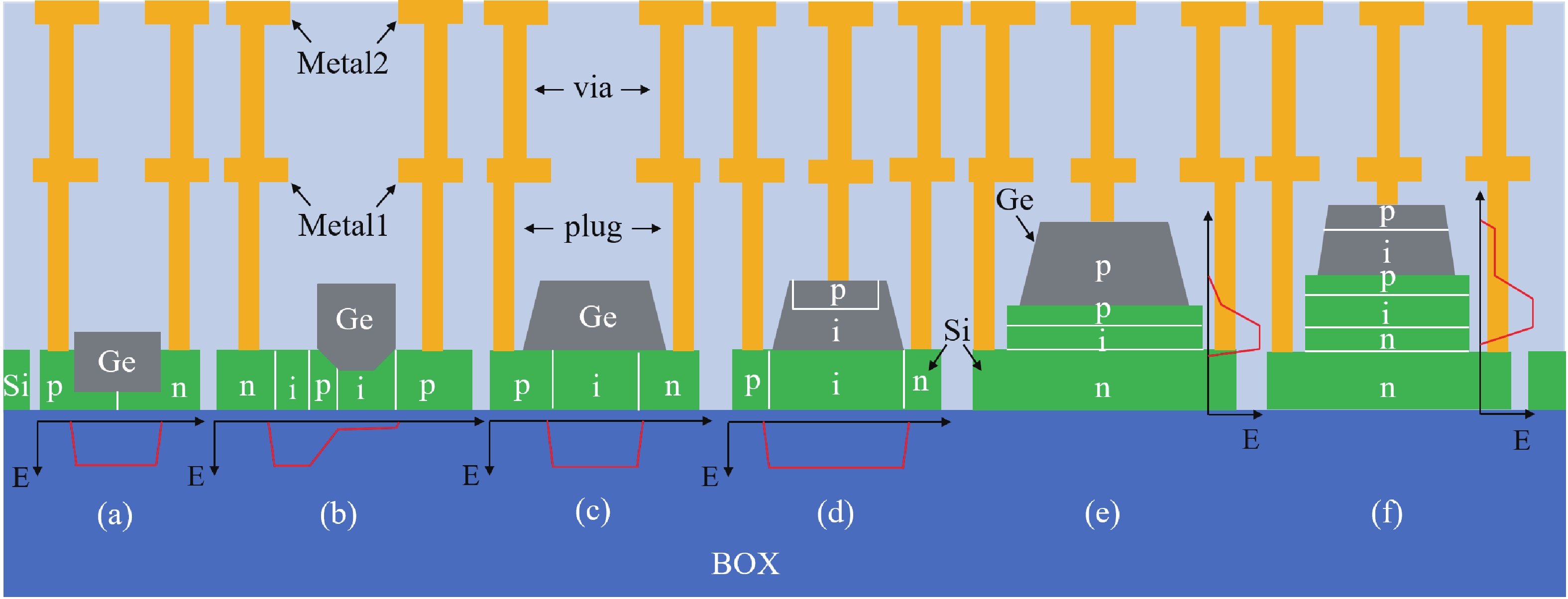
The excess noise factor increases with increasing gain M, while increases slower with lower k value. A low k means that electrons are much easier to get impact ionization than holes, reducing the stochastic gain fluctuations, thus the source of the excess noise is suppressed. In addition, Emmons has shown that low k value is also helpful for high gain-bandwidth product (GBP) in Ref. [17]. Consequently, a multiplication region with low k value is desired in APD. Due to similar electron and hole ionization coefficients for Ge, itsk value is close to unity (~ 0.9). Therefore, utilizing Ge as the absorption region and Si as the multiplication region can achieve advantages of both materials. Many device structures have been proposed for monolithic Si–Ge APDs, as shown in Fig. 1, from left to right, including lateral, hybrid vertical and lateral, and vertical structures.
![]()
Figure 1.(Color online) Common structures of Si–Ge APDs with E-field: (a) lateral p–i–n Si–Ge–Si APD[
Fig. 1(a) is a simple lateral p–i–n APD with a Si–Ge–Si heterojunction. The E-field at the Si–Ge interface is larger than that in the intrinsic Ge region, so that most impact ionization events occur at the interfaces of Si–Ge heterojunction and result in an effective k ~ 0.25[
![]()
Figure 2.(Color online)
In addition to concentrating the electric field to form the multiplication region inside low k value Si, the thickness of the multiplication region is also important. A thin multiplication region can reduce the carrier transit time, which is the premise of achieving high bandwidth. Besides that, the dead-space effect cannot be ignored. Unlike the excess noise local model of Eq. (2), a non-local model is necessary because the carrier history should be included for the thin multiplication region[
![]()
Figure 3.(Color online) (a) A cross-sectional structure, (b) a simulated E-field distribution, (c) a gain vs bandwidth plot, temperature-dependent characteristics of (d) gain and breakdown voltage, (e) bandwidth, and (f) 32 Gb/s NRZ and 64 Gb/s PAM4 eye diagrams of the 4 × 10
The 4 × 10 µm2 Si–Ge SACM APD has shown high-speed performance because the waveguide SACM structure decouples the photon absorption length (10 µm) in the wafer plane and carrier transit length (100 nm) normal to the wafer plane. However, there is still a trade-off between absorption length and RC time constant. To further loosen the trade-off, different simple Si mirrors have been integrated at the end of the Si–Ge waveguide APD to improve its responsivity without compromising the bandwidth[
![]()
Figure 4.(Color online) (a) Schematic of the Si–Ge APD with no reflector (Normal), a distributed Bragg reflector (DBR), and a loop reflector (LR), and (b) simulated absorption profiles. Comparison of (c) reflectivity, (d) photocurrent versus input power at unity gain point (e) impulse responses at gain ~ 10, 32 Gb/s NRZ bit error rate at bias voltage of (f) –8 V and (g) –10 V between the Normal, DBR1, DBR2, and LR APDs. (h) 40 Gb/s NRZ and 80 Gb/s PAM4 eye diagrams of the LR APD at bias of –10 V[
The enhanced responsivity can further improve the sensitivity of the low noise Si–Ge APDs. Figs. 4(f) and 4(g) show the comparison of their BERs at bias voltage of –8 and –10 V, respectively. A 32 Gb/s bit error rate tester was used to measure the BERs with 32 Gb/s NRZ operation. The BER of error-free transmission with KP4 forward error correction (FEC) is 2.4 × 10⁻⁴ as dash lines indicate in Figs. 4(f) and 4(g). At the bias of –8 V, Normal, DBR1, DBR2, and LR APDs achieve a sensitivity of ~ 11.7, –12.9, –13.3, and –13.4 dBm, respectively. The reflector-assisted APDs achieve 1–2 dB better sensitivity. Increasing the bias voltage to –10 V, Normal, DBR1, DBR2, and LR APDs obtain sensitivity of –15.0, –16.0, –15.9, and –15.7 dBm, respectively. And the APDs with reflector still allow ~ 1 dB better sensitivity. The high sensitivity Rx is desired in optical links, which can reduce the laser source power consumption and improve overall link energy efficiency. The Si–Ge waveguide APD with p–p–i–n SACM structure has been proved to have low excess noise, low operation voltage, high speed, high sensitivity, and excellent temperature stability characteristics. By adding the reflector at the end of the APD waveguide, the sensitivity can be further improved without changing any speed performance. We believe the high-performance Si–Ge SACM APD is an attractive Rx for future sub-pJ/bit optical links.
2.2. III–V APDs grown directly on silicon
III–V compound semiconductors have been widely used in active photonics devices due to their direct bandgaps, variable band structures, and flexible complex structure design. Integration of III–V semiconductors on Si has attracted significant interest as it can provide high-performance III–V photonics devices on SiPh platform, especially for lasers[
![]()
Figure 5.(Color online) Cross-sectional schematic of the InGaAs/InAlAs SACM APD directly on the InP/Si template[
The characteristics of the InGaAs/InAlAs SACM APD on Si are illustrated in Fig. 6. The I–V and gain curves of the APD on Si was measured at 1550 nm, the punch-through voltage is ~ –14 V and the highest gain is up to ~ 20. As shown in Fig. 6(b), the unity gain point responsivity of the top illuminated APD was measured with 1550 and 1310 nm light, where the captured responsivity is ~ 0.54 and 0.48 A/W, respectively. Considering the different wavelength photon energies, the corresponding external quantum efficiency is ~ 43% at 1550 nm and ~ 46 % at 1310 nm. Fig. 6(c) shows the excess noise performance, the k value of the III–V APD on Si is ~ 0.2. It is consistent with the reported value of the InP-based APD with comparable thick InAlAs multiplication region[
![]()
Figure 6.(Color online) (a)
where T is the absolute temperature,
2.3. III–V quantum dot APDs on silicon
While Ge on Si APDs and III–V on Si APDs have proved to be efficient detectors in silicon-based photonic integrated circuits for data communications, one of the main issues with these devices is their relatively high dark currents, which increases noise and limits sensitivity at high data rates. For example, dark current densities of 5 A/cm2 were measured for Ge-on-Si photodiodes operating at 1300 nm[
2.3.1. Heterogeneously integrated III–V quantum dot APDs on silicon
Since there is a large lattice constant mismatch between Si (a0 = 5.4310 Å) and most III–V compound semiconductors such as GaAs (a0 = 5.6533 Å), InP (a0 = 5.8687 Å) and InAs (a0 = 6.0584 Å), and mismatches in polarity and thermal expansion coefficients, directly growing these types of materials on silicon would create a large number of dislocations, significantly degrading the performance and increasing the dark current of photodiodes fabricated out of these materials, as discussed above. Thick buffer layers or other dislocation filtering or blocking techniques have been helpful to reduce the dislocation density down to ~106 cm–3, which is still a few orders of magnitude higher than the intrinsic value of epitaxial structures grow on a III–V native substrate. Thick buffer layers also prevent straightforward evanescent optical coupling between Si and III–V active region, which subsequently limits design flexibility of these devices in their integration with a silicon photonic integrated circuit. Heterogeneous integration offers the most practical and promising approach in the near-term to integrating high-performance III–V photonic devices directly onto silicon. This approach was discovered by Fang et al. in 2006 and since it has been developed and advanced significantly as a key technology for high-volume, low-cost on-chip active photonics, including photodetectors[
In particular, HPE has used this method to fabricate InAs QD avalanche photodiodes heterogeneously integrated on silicon[
![]()
Figure 7.(Color online) (a) Cross-section schematic of the photodiode. (b) SEM cross section of the QD waveguide PD on Si[
These APDs have shown the lowest dark current for any photodiode on silicon, as low as 10 pA (1 × 10⁻⁶ A/cm2) at –1 V for a 11 × 30 µm2 waveguide APD. Furthermore, the dark current density for a 11 × 60 µm2 device was 2.7 × 10⁻⁶ A/cm2 at –1 V and 3.4 × 10⁻⁶ A/cm2 at –1 V for a 11 × 90 µm2 device. The dark current scaling linearly with area suggests that the main contribution to the dark current comes from the bulk layers of the device. The low dark current is due to the combination of the 3-D carrier confinement of the QDs, good surface passivation of the PDs, low dislocation density and the high crystal quality of the active device material. Keeping the dark current low helps reduce the noise of the APD. The dark current was also measured as a function of temperature, as seen in Fig. 8(a). The breakdown voltage increases with temperature, implying that impact ionization is the main carrier mechanism behind the device breakdown.
![]()
Figure 8.(Color online) (a) Dark current vs. temperature for a 11 × 60
Device testing starts from light coming from an O-band tunable laser which was coupled into the grating coupler and the silicon waveguide then evanescently coupled into the APD. The spectral response in the O-band was taken for an 11 × 90 µm2 device and plotted in Fig. 8(b). There is both a wavelength and a bias dependence observed in the responsivity and gain of the device. This is accounted for by a combination of the avalanche gain and absorption of carriers within the device. As the wavelength of the input photons varies, the energy level of the photogenerated carriers within the QDs also varies. As carriers fill up the different energy levels, the carrier escape rates from the QDs change, altering the quantum efficiency, as well as the impact ionization rate of the carriers.
The responsivity at unity gain (–4 V) was 0.9 A/W at 1280 nm and 0.15 A/W at 1310 nm, implying a wavelength dependence on the absorption coefficient. At shorter wavelengths of the input optical mode, carriers are generated in the excited state within the QDs, and therefore, need less energy in order to escape the QDs. With the same bias voltage applied and an incoming 1310 nm optical signal, more carriers are generated in the ground state of the QD that need more energy in order to escape, causing a small amount of photocurrent being collected. Moreover, as the bias voltage increases, the absorption coefficient also shifts due to the quantum confined Stark effect (QCSE). The electron and hole wavefunctions inside the QDs shift with an increased in electric field applied, causing a subsequent shift in the absorption coefficient with wavelength[
The avalanche gain was measured and is shown in Fig. 8(c). With an input TE optical mode, a maximum gain of around 150 was measured at around –17.8 V, which is near the breakdown voltage. The polarization of the optical signal was then altered using a polarizer to change the input optical mode to the APD between TE and TM, and a polarization dependence on responsivity and gain was observed. With an input TM polarization, the gain increased by about a factor of 2 and the responsivity increased by a factor of 6. This is suggested to be due to a higher number of light holes being generated with TM polarization and then impact ionizing[
The high-speed dynamics was measured at –15, –16, and –17 V and can be seen in Fig. 8(d). These devices have also demonstrated a maximum 3-dB bandwidth of 20 GHz at and a maximum gain–bandwidth product (GBP) of 585 GHz, which is the record for III–V quantum dot APDs on silicon. 25 Gb/s open eye diagrams were also recorded (Fig. 8(e)) and a sensitivity of –11 dBm was measured at 10 Gb/s (Fig. 8(f)). Conclusively, III–V QD APDs heterogeneously integrated on silicon are still in their early stage of development but have a promising future as receivers in future WDM silicon photonic integrated circuits.
2.3.2. III–V quantum dot APDs monolithically grown on silicon
While wafer bonding has been successful in the development of high-performance III–V QD APDs on silicon, another promising approach is by monolithically growing III–V QD materials directly on silicon. The main advantages of this solution include ease of integration and scalability in regard to producing a large volume of devices on wafer. Also, due to the high defect sensitivity of QDs, the device performance will not be significantly reduced by dislocations. One way of growing III–V QD materials monolithically on Si is by using MBE and thick buffer layers. Another approach to this is by using metal organic chemical vapor deposition (MOCVD) and aspect ratio trapping. This method allows for the growth of GaAs on Si with a low defect density to produce QD avalanche photodiodes with low dark currents. Recently, there has been significant progress made on monolithically integrated QD APDs on silicon, which we discuss next.
The first InAs/GaAs QD photodetector monolithically integrated on silicon substrates was done using molecular beam epitaxy (MBE) by Wu et al.[
![]()
Figure 9.(Color online) (a) Schematic of wafer structure. (b) TEM image of the wafer[
Wan et al. fabricated p–i–n photodetectors from InAs/GaAs QDs directly grown on a GaAs-on-V-grooved-Si (GoVS)[
![]()
Figure 10.(Color online) (a) Schematic plot of the PD fabricated on the GoVS template. (b) Top-view and (c) cross-sectional view SEM images of a fabricated device[
Chen at al. measured device characteristics of InAs QD APDs grown with the same approach as Wan et al.[
![]()
Figure 11.(Color online) (a) Schematic diagram of the InAs QD APD grown on GoVS substrate. (b) APD gain versus the reverse bias at various temperatures. (c) Small-signal frequency response of the 3 × 50
While growth of these materials directly on silicon is being developed, APDs made from these materials are not quite ready for practical usage within industry for mass volume production. Some of the challenges consist of a limited understanding of the growth mechanics and physical carrier mechanisms of quantum dot lasers and photodetectors. And while offering plenty of advantages on a device level, we still need a better understanding of how to mitigate issues such as lifetime, repeatability, temperature sensitivity, and design flexibility. However, in the long term, this integration approach may likely be the preferred method of growth for quantum dot avalanche photodiodes on a silicon photonics platform for high-speed optical interconnects for data communication within data centers and HPC systems.
2.4. Comparison of APDs on silicon
Properties of different material APDs integrated on Si are summarized in chronological order as shown in Table 1. It includes Si–Ge, InGaAs-InAlAs, InAs QD, InAs-GaAs QD, and InAs-InGaAs QD material systems; where λ is the working wavelength, Vbr is the breakdown voltage, M is the highest gain, Idark is the dark current at unity gain, R is the responsivity at unity gain, BW is the highest bandwidth, GBP is the gain-bandwidth product, and BR is bit rate of eye diagrams.
Si–Ge APD is the most popular APD on SiPh platform due to the maturity of Ge growth technology on Si. Table 1 shows five different structures of Si–Ge APDs. The thin multiplication region of these Si–Ge APDs enables low breakdown voltage and high bandwidth. Besides that, the extremely low excess noise of Si makes Si–Ge APDs suitable for high bit rate operations. In contrast to Ge, most III–V semiconductors have much bigger lattice mismatch with Si. Therefore, a lot of effort has been put into heterogeneous or monolithic III–V on Si integration. For example, the bulk InGaAs–InAlAs material system have monolithically grown on Si to form SACM APDs. Although, several buffer layers are added to reduce the large lattice mismatch, the InGaAs-InAlAs APD on Si still shows much higher dark current than the same APD grown on InP. To alleviate the high dark current problem, QD is a promising material system for III–V APDs on Si. QD materials have a higher defect tolerance as a result of the strong localization of charges, which is particularly effective for the high dislocations problem in III–V on Si integration. In addition, QD itself has low dark current property due to the nature of three-dimensional confinement. As shown in Table 1, InAs QD, InAs-GaAs QD, and InAs-InGaAs QD APDs have been integrated on Si heterogeneously or monolithically. All of these QD APDs have much lower dark currents at unity gain compared to Si–Ge and bulk III–V APDs. However, QD APDs on Si still have some drawbacks that need to be improved. First, most integrated QD materials on Si have a relatively wide bandgap, resulting in a weak edge absorption around 1310 nm. Also due to the QCSE, the edge absorption coefficient changes with the electric field. Most current QD APDs on Si have a vertical p–i–n structure, such that light is absorbed and multiplicated in the same QD layer. It leads to high excess noise and a tighter trade-off between bandwidth and responsivity, which limits the high data rate performance.
Although the above material systems have been successfully monolithic or heterogeneous integrated on Si, APDs based on these materials still face challenges. For Si–Ge APDs, the dark current is still relatively high due to the lattice mismatch between Si and Ge. By further reducing misfits and threading dislocations at the Si–Ge interface, a dark current can be suppressed and thus enables better sensitivity. A similar problem of high dark current also exists for bulk III–V APDs on Si, requiring more efficient buffer layers to relive the stress between III–V and Si. Differently, QD APDs on Si are not sensitive to dislocations and thus have the ideal dark current. However, the speed, responsivity, and excess noise performance are not comparable to bulk semiconductor APDs. More optimized APD structures should be adopted to improve the overall performance of QD APDs.
3. Conclusion
In conclusion, we reviewed recent advances of the integrated APDs on silicon. The APDs on SiPh can leverage rewards of high-performance optical receivers and CMOS-compatible SiPh-integrated circuits, therefore provide an attractive Rx solution with standard manufacturing processes and low costs. One great advantage of APDs over PDs is its internal gain allows the optical links to have better SNR, which is crucial for many applications, such as future high-density, low-latency, and low-power optical interconnects. In past decades, numerous effort has been done to realize APDs on Si using monolithic or heterogeneous methods, and diverse semiconductor systems, including Si–Ge and III–V. Due to their great performance, especially the low excess noise and high sensitivity, integrated APDs will be of great use in a broad range of applications. It is not difficult to predict that high-quality APDs on Si will create a large market and become a powerful technology for explosive data growth.
References
[1] M Piels, J E Bowers. Photodetectors for silicon photonic integrated circuits. Photodetectors. Amsterdam: Elsevier, 3(2016).
[2] J M Fédéli, L Virot, L Vivien et al. High-performance waveguide-integrated germanium PIN photodiodes for optical communication applications. 2014 7th Int Silicon Ger Technol Device Meet ISTDM, 131(2014).
[3] L Virot, D Benedikovic, B Szelag et al. Integrated waveguide PIN photodiodes exploiting lateral Si/Ge/Si heterojunction. Opt Express, 25, 19487(2017).
[4] K Y Sun, T C Tzu, R Costanzo et al. Ge-on-Si balanced periodic traveling-wave photodetector. 2019 IEEE Photonics Conference (IPC), 1(2019).
[5] L Bogaert, K van Gasse, T Spuesens et al. Silicon photonics traveling wave photodiode with integrated star coupler for high-linearity mm-wave applications. Opt Express, 26, 34763(2018).
[6] X J Xie, Q G Zhou, E Norberg et al. High-power and high-speed heterogeneously integrated waveguide-coupled photodiodes on silicon-on-insulator. J Lightwave Technol, 34, 73(2016).
[7] G Muliuk, J Zhang, J Goyvaerts et al. High-yield parallel transfer print integration of III-V substrate-illuminated C-band photodiodes on silicon photonic integrated circuits. Proc SPIE 10923, Silicon Photonics XIV, 1092(2019).
[8] K Y Sun, D Jung, C Shang et al. Low dark current III–V on silicon photodiodes by heteroepitaxy. Opt Express, 26, 13605(2018).
[9] K Y Sun, J Y Gao, D Jung et al. 40 Gbit/s waveguide photodiode using III–V on silicon heteroepitaxy. Opt Lett, 45, 2954(2020).
[10] M Casalino, M Iodice, L Sirleto et al. Asymmetric MSM sub-bandgap all-silicon photodetector with low dark current. Opt Express, 21, 28072(2013).
[11] H Cansizoglu, A S Mayet, S Ghandiparsi et al. Dramatically enhanced efficiency in ultra-fast silicon MSM photodiodes via light trapping structures. IEEE Photonics Technol Lett, 31, 1619(2019).
[12] D Akinwande, C Huyghebaert, C H Wang et al. Graphene and two-dimensional materials for silicon technology. Nature, 573, 507(2019).
[13] J F Gonzalez Marin, D Unuchek, K Watanabe et al. MoS2 photodetectors integrated with photonic circuits. npj 2D Mater Appl, 3, 1(2019).
[14] J C Campbell. Recent advances in avalanche photodiodes. J Lightwave Technol, 34, 278(2016).
[15] D Benedikovic, L Virot, G Aubin et al. Silicon–germanium receivers for short-wave-infrared optoelectronics and communications. Nanophotonics, 10, 1059(2021).
[16] R J McIntyre. Multiplication noise in uniform avalanche diodes. IEEE Trans Electron Devices, ED-13,164(1966).
[17] R B Emmons. Avalanche-photodiode frequency response. J Appl Phys, 38, 3705(1967).
[18] D Benedikovic, L Virot, G Aubin et al. 40 Gbps heterostructure germanium avalanche photo receiver on a silicon chip. Optica, 7, 775(2020).
[19] S A Srinivasan, M Berciano, P de Heyn et al. 27 GHz silicon-contacted waveguide-coupled Ge/Si avalanche photodiode. J Lightwave Technol, 38, 3044(2020).
[20] J Zhang, B P P Kuo, S Radic. 64Gb/s PAM4 and 160Gb/s 16QAM modulation reception using a low-voltage Si-Ge waveguide-integrated APD. Opt Express, 28, 23266(2020).
[21] X G Zeng, Z H Huang, B H Wang et al. Silicon–germanium avalanche photodiodes with direct control of electric field in charge multiplication region. Optica, 6, 772(2019).
[22] Z H Huang, C Li, D Liang et al. 25 Gbps low-voltage waveguide Si–Ge avalanche photodiode. Optica, 3, 793(2016).
[23] Y M Kang, H D Liu, M Morse et al. Monolithic germanium/silicon avalanche photodiodes with 340 GHz gain-bandwidth product. Nat Photonics, 3, 59(2009).
[24]
[25] X W Li, X G Zheng, S L Wang et al. Calculation of gain and noise with dead space for GaAs and Al
[26] G J Rees, J R David. Nonlocal impact ionization and avalanche multiplication. J Phys D, 43, 243001(2010).
[27] E Jamil, J S Cheong, J P David et al. On the analytical formulation of excess noise in avalanche photodiodes with dead space. Opt Express, 24, 21597(2016).
[28] Y Yuan, Z H Huang, B H Wang et al. 64 Gbps PAM4 Si-Ge waveguide avalanche photodiodes with excellent temperature stability. J Lightwave Technol, 38, 4857(2020).
[29] C N Harrison, J P R David, M Hopkinson et al. Temperature dependence of avalanche multiplication in submicron Al0.6Ga0.4As diodes. J Appl Phys, 92, 7684(2002).
[30] A H Jones, Y Yuan, M Ren et al. Al
[31]
[32] B H Wang, Z H Huang, Y Yuan et al. 64 Gb/s low-voltage waveguide SiGe avalanche photodiodes with distributed Bragg reflectors. Photon Res, 8, 1118(2020).
[33] Y Yuan, Z H Huang, X G Zeng et al. High responsivity Si-Ge waveguide avalanche photodiodes enhanced by loop reflector. IEEE J Sel Top Quantum Electron, 28, 1(2022).
[34] A Y Liu, J Bowers. Photonic integration with epitaxial III–V on silicon. IEEE J Sel Top Quantum Electron, 24, 1(2018).
[35] Y Han, Y Xue, Z Yan et al. Selectively grown III-V lasers for integrated Si-photonics. J Lightwave Technol, 39, 940(2021).
[36] D Liang, J E Bowers. Recent progress in heterogeneous III-V-on-silicon photonic integration. Light: Adv Manuf, 2, 1(2021).
[37] N Li, R Sidhu, X W Li et al. InGaAs/InAlAs avalanche photodiode with undepleted absorber. Appl Phys Lett, 82, 2175(2003).
[38] M Nada, H Yokoyama, Y Muramoto et al. A 50-Gbit/s vertical illumination avalanche photodiode for 400-Gbit/s Ethernet systems. Opt Express, 22, 14681(2014).
[39] M Nada, M Nakamura, H Matsuzaki. 25-Gbit/s burst-mode optical receiver using high-speed avalanche photodiode for 100-Gbit/s optical packet switching. Opt Express, 22, 443(2014).
[40] Y L Zhao, D D Zhang, L Qin et al. InGaAs–InP avalanche photodiodes with dark current limited by generation-recombination. Opt Express, 19, 8546(2011).
[41] X Meng, C H Tan, S Dimler et al. 1550 nm InGaAs/InAlAs single photon avalanche diode at room temperature. Opt Express, 22, 22608(2014).
[42] M G Liu, C Hu, X G Bai et al. High-performance InGaAs/InP single-photon avalanche photodiode. IEEE J Sel Top Quantum Electron, 13, 887(2007).
[43] M Ren, X R Gu, Y Liang et al. Laser ranging at 1550 nm with 1-GHz sine-wave gated InGaAs/InP APD single-photon detector. Opt Express, 19, 13497(2011).
[44] X B Liu, Li Li. Design of the optical system of flash lidar based on an APD array. Infrared Laser Eng, 38, 893(2009).
[45] B Schwarz. Mapping the world in 3D. Nat Photonics, 4, 429(2010).
[46] G Adamo, A Busacca. Time of flight measurements via two LiDAR systems with SiPM and APD. 2016 AEIT International Annual Conference (AEIT)(2016).
[47] A W Elshaari, W Pernice, K Srinivasan et al. Hybrid integrated quantum photonic circuits. Nat Photonics, 14, 285(2020).
[48]
[49] S Keyvaninia, M Muneeb, S Stanković et al. Ultra-thin DVS-BCB adhesive bonding of III-V wafers, dies and multiple dies to a patterned silicon-on-insulator substrate. Opt Mater Express, 3, 35(2012).
[50] J Zhang, G Muliuk, J Juvert et al. III-V-on-Si photonic integrated circuits realized using micro-transfer-printing. APL Photonics, 4, 110803(2019).
[51] I Lucci, S Charbonnier, L Pedesseau et al. Universal description of III-V/Si epitaxial growth processes. Phys Rev Materials, 2, 060401(2018).
[52] Y Yuan, D Jung, K Sun et al. III-V on silicon avalanche photodiodes by heteroepitaxy. Opt Lett, 44, 3538(2019).
[53] T Nakata, J Ishihara, K Makita et al. Multiplication noise characterization of InAlAs-APD with heterojunction. IEEE Photonics Technol Lett, 21, 1852(2009).
[54] M Jutzi, M Berroth, G Wöhl et al. Zero biased Ge-on-Si photodetector on a thin buffer with a bandwidth of 3.2 GHz at 1300 nm. Mater Sci Semicond Process, 8, 423(2005).
[55] L Colace, P Ferrara, G Assanto et al. Low dark-current germanium-on-silicon near-infrared detectors. IEEE Photonics Technol Lett, 19, 1813(2007).
[56] B Tossoun, G Kurczvcil, C Zhang et al. High-speed 1310 nm hybrid silicon quantum dot photodiodes with ultra-low dark current. 2018 76th Device Research Conference (DRC), 1(2018).
[57] A W Fang, H Park, R Jones et al. A continuous-wave hybrid AlGaInAs-silicon evanescent laser. IEEE Photon Technol Lett, 18, 1143(2006).
[58] J E Bowers. Evolution of photonic integrated circuits. 2017 75th Annual Device Research Conference (DRC), 1(2017).
[59] B Tossoun, G Kurczveil, C Zhang et al. Indium arsenide quantum dot waveguide photodiodes heterogeneously integrated on silicon. Optica, 6, 1277(2019).
[60] B Tossoun, S Srinivasan, A Descos et al. High-speed heterogeneous quantum dot avalanche photodiodes with polarization dependent gain. 2020 IEEE Photonics Conference (IPC), 1(2020).
[61] B Tossoun, G Kurczveil, S Srinivasan et al. 32 Gbps heterogeneously integrated quantum dot waveguide avalanche photodiodes on silicon. Opt Lett, 46, 3821(2021).
[62] H Ishikawa, H Shoji, Y Nakata et al. Self-organized quantum dots and quantum dot lasers. J Vac Sci Technol A, 16, 794(1998).
[63] D Liang, J E Bowers. Highly efficient vertical outgassing channels for low-temperature InP-to-silicon direct wafer bonding on the silicon-on-insulator substrate. J Vac Sci Technol B, 26, 1560(2008).
[64] P Jin, C M Li, Z Y Zhang et al. Quantum-confined Stark effect and built-in dipole moment in self-assembled InAs∕GaAs quantum dots. Appl Phys Lett, 85, 2791(2004).
[65] T Umezawa, K Akahane, A Matsumoto et al. Polarization dependence of avalanche multiplication factor in 1.5 μm quantum dot waveguide photodetector. Conference on Lasers and Electro-Optics(2016).
[66] J Wu, Q Jiang, S M Chen et al. Monolithically integrated InAs/GaAs quantum dot mid-infrared photodetectors on silicon substrates. ACS Photonics, 3, 749(2016).
[67] I Sandall, J S Ng, J P R David et al. 1300 nm wavelength InAs quantum dot photodetector grown on silicon. Opt Express, 20, 10446(2012).
[68] Y T Wan, Z Y Zhang, R L Chao et al. Monolithically integrated InAs/InGaAs quantum dot photodetectors on silicon substrates. Opt Express, 25, 27715(2017).
[69] B L Chen, Y T Wan, Z Y Xie et al. Low dark current high gain InAs quantum dot avalanche photodiodes monolithically grown on Si. ACS Photonics, 7, 528(2020).
[70] A Pauchard, M Bitter, D Sengupta et al. High-performance InGaAs-on-silicon avalanche photodiodes. Optical Fiber Communication Conference and Exhibit, 345(2002).
[71] T Umezawa, K Akahane, A Kanno et al. Investigation of a 1.5-µm-wavelength InAs-quantum-dot absorption layer for high-speed photodetector. Appl Phys Express, 7, 032201(2014).

Set citation alerts for the article
Please enter your email address
© Copyright 2018-2021 | Chinese Laser Press. All Rights Reserved 沪ICP备15018463号-20